
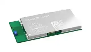


ENW49C02A3KF
Wi-Fi Embedded b/g/n Module, 2x UART, 3V to 3.6V Supply, 1Mbps, -97dBm Sensitivity
- Manufacturer: PANASONIC
- Product type:
- Frequency RF:2.4GHz; Module Interface:UART; Module Applications:IoT, Multimedia, Home Electronics, Home Appliances & White Goods, Industrial & Home Automation; Product Range:PAN9420, PA
- SVHC: No SVHC (25-Jun-2025)
- Frequency RF: 2.4GHz
- Product Range: PAN9420, PAN9320
- Module Interface: UART
- Module Applications: IoT, Multimedia, Home Electronics, Home Appliances & White Goods, Industrial & Home Automation
| Delivery and price | |
|---|---|
| Units per pack | 250 |
| Price | 14.69 € |
| Current stock | 10+ |
| Lead time | 30 days |
## Panasonic ## PAN9420 Fully Embedded Stand-Alone Wi-Fi Module Product Specification Rev. 1.2 PAN9420 Wi-Fi Module ## ## **Overview** The PAN9420 is a 2.4 GHz ISM band Wi-Fi-embedded module which includes a wireless radio and an MCU for easy integration of Wi-Fi connectivity into various electronic devices. ## **Features** - [Fully embedded: integrated][full-featured network ] stack - [Contains all necessary IoT functionality (Place & ] Play) - [Integrated webserver with AJAX/JSON for web ] applications - [No stack or software implementation needed on ] a host MCU - [Simultaneous support of Access-Point- & ] Infrastructure mode - [Fully automatical IP configuration ] - [DHCP server offers IP configuration in AP mode ] - [Access by names (http://yourdevice) ] - [Integrated TCP/IP network stack: IPv4, ARP, ] and AutoIP - [Supports TLS/SSL, https, and Wi-Fi security ] (WPA2) for secure data connection - [Over-the-Air firmware update ] - [Two UART interfaces (command and ] transparent data) - [Integrated QSPI flash memory for customer web ] contents and configuration file - [• ][Programming via standard JTAG ] - [Evaluation kit with pre-installed web application for ] quick prototyping available - [Evaluation and development tool WiFigurator for ] Windows - [Getting started tutorials, PC tool, quickstart guide ] - [Wide temperature range of -40 °C to +85 °C] ## **Characteristics** - [Surface Mount Type (SMT) ] 29.0 mm x 13.5 mm x 2.66 mm - [Marvell® 88MW300 MCU/WLAN System-on-Chip ] (SoC) inside - [Tx power up to +16 dBm @ IEEE 802.11b ] - [Rx sensitivity of -97 dBm @ IEEE 802.11b DSSS ] 1 Mbps - [20 MHz channels up to 72 Mbps ] - [Power supply 3.0 to 3.6 V ] - [Current consumption 150 mA (mix mode ] Tx/Rx @ 11b, 11 Mbps), 75 mA Rx, 310 mA Tx peak - [Power down mode < 1 mA power consumption ] - [Low power mode available ] ## **Delta PAN9420 vs PAN9320** - [PAN9320 replaceable by PAN9420 without ] changes on mother PCB - [Reduced power consumption in transmit, idle, and ] power down - [Enhanced temperature range of -40 °C to +85 °C ] ## **Block Diagram** **==> picture [291 x 200] intentionally omitted <==** **----- Start of picture text -----**<br> Vcc 3.3 V PAN9420<br>QSPI Flash Fully Embedded Wi-Fi Module<br>SPI 32 Mbit IEEE 802.11 b/g/n<br>UART0<br>UART1<br>Crystal<br>GPIOs 38.4 MHz<br>JTAG Chip<br>Antenna<br>Status LEDs Crystal<br>32.768 kHz<br>88MW300<br>MCU Ready MCU/Radio SoC<br>Resetn<br>Factory Reset<br>Wake Ups LPF SPDT<br>V SPDT<br>RF-Pad<br>**----- End of picture text -----**<br> Product Specification Rev. 1.1 Page 2 PAN9420 Wi-Fi Module By purchase of any of the products described in this document the customer accepts the document's validity and declares their agreement and understanding of its contents and recommendations. Panasonic reserves the right to make changes as required at any time without notification. Please consult the most recently issued Product Specification before initiating or completing a design. © Panasonic Industrial Devices Europe GmbH 2017. This specification sheet is copyrighted. Reproduction of this document is permissible only if reproduction is without alteration and is accompanied by all associated warranties, conditions, limitations, and notices. Do not disclose it to a third party. All rights reserved. This Product Specification does not lodge the claim to be complete and free of mistakes. ## **Engineering Samples (ES)** If Engineering Samples are delivered to the customer, these samples have the status “Engineering Samples”. This means that the design of this product is not yet concluded. Engineering Samples may be partially or fully functional, and they may differ from the published Product Specification. Engineering Samples are not qualified and they are not to be used for reliability testing or series production. ## **Disclaimer** The customer acknowledges that samples may deviate from the Product Specification and may bear defects due to their status of development and the lack of qualification mentioned above. Panasonic rejects any liability or product warranty for Engineering Samples. In particular, Panasonic disclaims liability for damages caused by: The use of the Engineering Sample other than for evaluation purposes, particularly the installation or integration in another product to be sold by the customer, Deviation or lapse in function of the Engineering Sample, Improper use of the Engineering Sample. Panasonic Industrial Devices Europe GmbH disclaims any liability for consequential and incidental damages. In case of any queries regarding the Engineering Samples, please contact your local sales partner or the related product manager. Product Specification Rev. 1.1 Page 3 PAN9420 Wi-Fi Module ## ## **Table of Contents** |**1**|**About**|**This Document ......................................................................................................................... 5**| |---|---|---| ||1.1|Purpose and Audience .............................................................................................................. 5| ||1.2|Revision History ......................................................................................................................... 5| ||1.3|Use of Symbols ......................................................................................................................... 5| ||1.4|Related Documents ................................................................................................................... 5| |**2**|**Overview .............................................................................................................................................. 6**|| ||2.1|Block Diagram ........................................................................................................................... 7| ||2.2|Pin Configuration ....................................................................................................................... 8| ||2.3|Host Interfaces ........................................................................................................................ 11| ||2.4|Peripheral Bus Interface .......................................................................................................... 11| ||2.5|WLAN Features ....................................................................................................................... 12| |**3**|**Detailed Description ......................................................................................................................... 14**|| ||3.1|Dimensions .............................................................................................................................. 14| ||3.2|Footprint .................................................................................................................................. 15| ||3.3|Packaging ................................................................................................................................ 16| ||3.4|Case Marking .......................................................................................................................... 19| |**4**|**Specification ..................................................................................................................................... 20**|| ||4.1|Default Test Conditions ........................................................................................................... 20| ||4.2|Absolute Maximum Ratings ..................................................................................................... 20| ||4.3|Recommended Operating Conditions ...................................................................................... 21| ||4.4|RF Electrical Characteristics .................................................................................................... 29| ||4.5|Reliability Tests ....................................................................................................................... 33| ||4.6|Recommended Soldering Profile ............................................................................................. 34| |**5**|**Cautions ............................................................................................................................................ 35**|| ||5.1|Design Notes ........................................................................................................................... 35| ||5.2|Installation Notes ..................................................................................................................... 35| ||5.3|Usage Condition Notes ............................................................................................................ 36| ||5.4|Storage Notes .......................................................................................................................... 36| ||5.5|Safety Cautions ....................................................................................................................... 36| ||5.6|Other Cautions ........................................................................................................................ 37| ||5.7|Life Support Policy ................................................................................................................... 37| |**6**|**Regulatory and Certification Information ....................................................................................... 38**|| ||6.1|Federal Communications Commission (FCC) for US .............................................................. 38| ||6.2|Innovation, Science, and Economic Development (ISED) for Canada .................................... 40| ||6.3|European Conformity According to RED (2014/53/EU) ........................................................... 43| ||6.4|RoHS and REACH Declaration ............................................................................................... 43| |**7**|**Appendix ........................................................................................................................................... 44**|| ||7.1|Ordering Information ................................................................................................................ 44| ||7.2|Contact Details ........................................................................................................................ 45| Product Specification Rev. 1.1 Page 4 PAN9420 Wi-Fi Module 1 About This Document ## **1 About This Document** ## **1.1 Purpose and Audience** This Product Specification provides details on the functional, operational, and electrical characteristics of the Panasonic PAN9420 module. It is intended for hardware design, application, and Original Equipment Manufacturers (OEM) engineers. The product is referred to as “the PAN9420” or “the module” within this document. ## **1.2 Revision History** |**Revision**|**Date**|**Modifications/Remarks**| |---|---|---| |0.1|01.02.2017|1st preliminary version| |0.2|31.05.2017|Improved layout| |1.0|02.06.2017|Technical data corrected| |1.1|19.06.2017|FCC/IC/RED information added| |1.2|29.09.2017|Add technical data| ## **1.3 Use of Symbols** |**Symbol**|**Description**| |---|---| |@|**Note**<br>Indicates important information for the proper use of the product.<br>Non-observance can lead to errors.| |A|**Attention**<br>Indicates important notes that, if not observed, can put the product’s functionality<br>at risk.| |[chapter number]<br>[chapter title]|**Cross reference**<br>Indicates cross references within the document.<br>**Example:**<br>Description of the symbols used in this document1.3 Use of Symbols.| ## **1.4 Related Documents** Please refer to the Panasonic website for related documents 7.2.2 Product Information. Product Specification Rev. 1.1 Page 5 PAN9420 Wi-Fi Module 2 Overview ## **2 Overview** The PAN9420 is a 2.4 GHz 802.11 b/g/n embedded Wi-Fi module with integrated stack and API that minimizes firmware development and includes a full security suite. The module is specifically designed for highly integrated and cost-effective applications. The module includes a fully shielded case, integrated crystal oscillators, and a chip antenna. The module combines a high-performance CPU, high-sensitivity wireless radio, baseband processor, medium access controller, encryption unit, boot ROM with patching capability, internal SRAM, and in-system programmable flash memory. The module’s integrated memory is available to the application for storing web content such as HTML pages or image data. Parallel support of access point and infrastructure mode allows easy setup of simultaneous Wi-Fi connections from the module to smart devices and home network routers. The pre-programmed Wi-Fi SoC firmware enables client (STA), micro access point (uAP), and Ad-hoc mode (Wi-Fi Direct) applications. With the transparent mode, raw data can be sent from the UART to the air interface to smart devices, web servers, or PC applications. The PAN9420 supports Over-the-Air firmware updates. In order to make use of this feature, the customer needs to ensure that the appropriate preconditions are fulfilled and that a suitable environment is provided, particularly with regard to: - Module configuration - Utilization of the related module interface commands - Server infrastructure and application Please refer to the Panasonic website for related documents 7.2.2 Product Information. Further information on the variants and versions 7.1 Ordering Information. Product Specification Rev. 1.1 Page 6 PAN9420 Wi-Fi Module 2 Overview ## **2.1 Block Diagram** **==> picture [415 x 285] intentionally omitted <==** **----- Start of picture text -----**<br> Vcc 3.3 V PAN9420<br>QSPI Flash Fully Embedded Wi-Fi Module<br>SPI<br>32 Mbit IEEE 802.11 b/g/n<br>UART0<br>UART1<br>Crystal<br>GPIOs 38.4 MHz<br>Chip<br>JTAG<br>Antenna<br>Status LEDs Crystal<br>32.768 kHz<br>88MW300<br>MCU Ready<br>MCU/Radio SoC<br>Resetn<br>Factory Reset<br>Wake Ups LPF SPDT<br>V SPDT<br>RF-Pad<br>**----- End of picture text -----**<br> Product Specification Rev. 1.1 Page 7 PAN9420 Wi-Fi Module 2 Overview ## **2.2 Pin Configuration** ## **Pin Assignment** ## **Pin Functions** |**No**|**Pin Name**|**Pin Type**|**Description**| |---|---|---|---| |1 GND|1 GND|Ground Pin|Connect to ground| |2 GPIO4|2 GPIO41|Digital I/O|Digital I/O #4| |3 GPIO5<br>~~ee~~|3 GPIO51<br>~~ee~~|Digital I/O<br>~~ee~~|Digital I/O #5<br>~~ee~~| |4 NC<br>~~ee~~<br>~~a~~|4 NC<br>~~ee~~<br>~~a~~|NC<br>~~ee~~<br>|Do not connect<br>~~ee~~<br>| |5 NC<br>~~aee~~|5 NC<br>~~aee~~|NC<br>~~ee~~|Do not connect<br>~~ee~~| |6 NC<br>~~ee~~<br>~~ee~~|6 NC<br>~~ee~~<br>~~ee~~|NC<br>~~ee~~<br>~~ee~~|Do not connect<br>~~ee~~<br>~~ee~~| |7 3.3 V<br>~~ee~~<br>~~ee~~|7 3.3 V<br>~~ee~~<br>~~ee~~|Power<br>~~ee~~<br>~~ee~~|3.0 V-3.6 V power supply connection (typical 3.3 V)<br>~~ee~~<br>~~ee~~| |8 3.3 V<br>~~ee~~<br>~~ee~~|8 3.3 V<br>~~ee~~<br>~~ee~~|Power<br>~~ee~~<br>~~ee~~|3.0 V-3.6 V power supply connection (typical 3.3 V)<br>~~ee~~<br>~~ee~~| |9 UART1 CTS<br>~~ee~~<br>~~ee~~|9 UART1 CTS<br>~~ee~~<br>~~ee~~|Digital In<br>~~ee~~<br>~~ee~~|CTSn for UART1 (using hardware flow control)<br>~~ee~~<br>~~ee~~| |10 UART1 RTS<br>~~ee~~<br>~~ee~~|10 UART1 RTS<br>~~ee~~<br>~~ee~~|Digital Out<br>~~ee~~<br>~~ee~~|RTSn for UART1 (using hardware flow control)<br>~~ee~~<br>~~ee~~| |11 UART1 TXD<br>~~ee~~<br>~~ee~~|11 UART1 TXD<br>~~ee~~<br>~~ee~~|Digital Out<br>~~ee~~<br>~~ee~~|TXD for UART1<br>~~ee~~<br>~~ee~~| |12 UART1 RXD<br>~~ee~~<br>~~ee~~|12 UART1 RXD<br>~~ee~~<br>~~ee~~|Digital In<br>~~ee~~<br>~~ee~~|RXD for UART1<br>~~ee~~<br>~~ee~~| |13 NC<br>~~ee~~|13 NC<br>~~ee~~|NC<br>~~ee~~|Do not connect<br>~~ee~~| |14 GND|14 GND|Ground Pin|Connect to ground| |15 GND<br>~~e~~|15 GND<br>~~e~~|Ground Pin<br>~~e~~|Connect to ground<br>~~ee~~| 1 All GPIOs are initially set to output with low level Product Specification Rev. 1.1 Page 8 PAN9420 Wi-Fi Module 2 Overview |**No**|**Pin Name**|**Pin Type**|**Description**| |---|---|---|---| ||||| |16|NC/RF|NC/Analog IO|RF in/out over 50Ω bottom pad| |17|GND|Ground Pin|Connect to ground| |18|GND|Ground Pin|Connect to ground| |19|GND|Ground Pin|Connect to ground| |20|GND|Ground Pin|Connect to ground| |21|GND|Ground Pin|Connect to ground| |22|GND|Ground Pin|Connect to ground| |23|GND|Ground Pin|Connect to ground| |24|GND|Ground Pin|Connect to ground| |25|GND|Ground Pin|Connect to ground| |26|W STAT LED|Digital Out|Connect to LED wireless (Wi-Fi) status, active low| |27|UART0 TXD/DUAL STAT|Digital Out|TXD for UART0/UART1 state (binary data or command)| |28|UART0 RXD/DUAL SW|Digital In|RXD for UART0/UART1 toggle switch for the control of the state| |29|GPIO491|Digital I/O|Digital I/O #49| |30|GPIO481|Digital I/O|Digital I/O #48| |31|GPIO471|Digital I/O|Digital I/O #47| |32|GPIO461|Digital I/O|Digital I/O #46| |33|STAT LED1|Digital Out|Connect to LED MCU status (heartbeat), active low| |34|STAT LED2|Digital Out|Connect to LED IP connectivity (allocated IP), active low| |35|STAT LED3|Digital Out|Connect to LED Error (active during booting), active low| |36|GND|Ground Pin|Connect to ground| |37|RESETn|Digital In|Reset MCU, active low| |38|WAKE UP02|Digital In|Wake up signal for MCU/WLAN SoC, active high| |39|NC|NC|Do not connect| |40|NC|NC|Do not connect| |41|MCU READY|Digital Out|Connect to LED MCU ready (booting ready), active high| |42|FACTORY RESET|Digital In|Factory reset (valid after 10 seconds), active high| |A1|NC|NC|Do not connect| |A2|NC|NC|Do not connect| |A3|NC|NC|Do not connect| |A4|SPDT V1|Input Signal|Do not connect if on-board antenna In/Out is desired, for RF-Pad<br>In/Out4.3.2 Module Selectable RF-In/Output.| > 2 Connect to HOST MCU (wake up after shut-off mode, active high), use 10 kOhm resistor to GND at pin Product Specification Rev. 1.1 Page 9 PAN9420 Wi-Fi Module 2 Overview |**No**|**Pin Name**|**Pin Type**|**Description**| |---|---|---|---| ||||| |A5|SPDT V2|Input Signal|Do not connect if on-board antenna In/Out is desired, for RF-Pad<br>In/Out4.3.2 Module Selectable RF-In/Output.| |B1|NC|NC|Do not connect| |B2|NC|NC|Do not connect| |B3|NC|NC|Do not connect| |B4|NC|NC|Do not connect| |B5|NC|NC|Do not connect| |C1|NC|NC|Do not connect| |C2|NC|NC|Do not connect| |C3|WAKE UP12|Digital In|Wake up signal for MCU/WLAN SoC, active high| |C4|NC|NC|Do not connect| |C5|NC|NC|Do not connect| |D1|TDI|Digital In|TDI for JTAG (option for flashing in production process)| |D2|TRSTn|Digital In|TRSTn for JTAG (option for flashing in production process)| |D3|NC|NC|Do not connect| |D4|NC|NC|Do not connect| |D5|NC|NC|Do not connect| |E1|TDO|Digital Out|TDO for JTAG (option for flashing in production process)| |E2|TCK|Digital Out|TCK for JTAG (option for flashing in production process)| |E3|TMS|Digital I/O|TMS for JTAG (option for flashing in production process)| |E4|NC|NC|Do not connect| |E5|NC|NC|Do not connect| |F1|NC|NC|Do not connect| |F2|NC|NC|Do not connect| |F3|GND|Ground Pin|Connect to ground| |F4|GND|Ground Pin|Connect to ground| |F5|GND|Ground Pin|Connect to ground| |GND THERMO||Thermal Pin|Connect to ground| |GND THERMO||Thermal Pin|Connect to ground| |GND THERMO||Thermal Pin|Connect to ground| |GND THERMO||Thermal Pin|Connect to ground| Product Specification Rev. 1.1 Page 10 PAN9420 Wi-Fi Module 2 Overview ## **2.3 Host Interfaces** ## **UART0 Interface** - 2-wire data transfer (RX, TX) - Programmable baud rate (300 bps to 1.5 Mbps) - Data format (LSB first) - Data bit: (5-8 bit) - Parity bit: (0-3 bit) - Stop bit: (1-2 bit) ## **UART1 Interface** - 4-wire data transfer (RX, TX, RTS, CTS) - Programmable baud rate (300 bps to 1.5 Mbps) - Data format (LSB first) - Data bit: (5-8 bit) - Parity bit: (0-3 bit) - Stop bit: (1-2 bit) Further information 4.3.7 Host Interface Specification. ## **2.4 Peripheral Bus Interface** ## **Embedded MCU and WLAN Radio (SoC)** |**Features**|**Characteristics**| |---|---| ||| |JTAG|•Standard JTAG interface| |General Purpose I/O<br>(GPIO) Interface|•Defined GPIOs, I/O configured to either input or output (on/off)<br>•GPIOs with LED status functionality (ready, heartbeat, IP-connectivity,<br>error and WLAN connectivity)| |Wake Up 0 / 1|•External signal for wake-up after shut-off mode| Further information 4.3.8 Peripheral Interface Specification. Product Specification Rev. 1.1 Page 11 PAN9420 Wi-Fi Module 2 Overview ## **2.5 WLAN Features** |**Type**|**Features**| |---|---| ||| |IEEE 802.11/Standards|•802.11 data rates 1 and 2 Mbps (DSSS)<br>•802.11b data rates 5.5 and 11 Mbps (CCK)<br>•802.11g data rates 6, 9, 12, 18, 24, 36, 48, and 54 Mbps (OFDM)<br>•802.11b/g performance enhancements<br>•802.11n-compliant with maximum data rates up to 72 Mbps<br>(20 MHz channel)<br>•802.11d international roaming3<br>•802.11i enhanced security<br>•802.11k radio resource measurement3<br>•802.11r fast hand-off for AP roaming3<br>•802.11w protected management frames3<br>•Support clients (stations) implementing IEEE Power Save mode<br>•Wi-Fi direct connectivity3| |WLAN MAC|•Simultaneous peer-to-peer and Infrastructure Modes<br>•RTS/CTS for operation and DCF<br>•Hardware filtering of 32 multicast addresses<br>•On-chip Tx and Rx FIFO for maximum throughput<br>•Open System and Shared Key Authentication services<br>•A-MPDU RX (de-aggregation) and TX (aggregation)<br>•Reduced Inter-Frame Spacing (RIFS) bursting<br>•Management information base counters<br>•Radio resource measurement counters<br>•Quality of service queues<br>•Block acknowledgement extensions<br>•Multiple-BSSID and Multiple-Station operation<br>•Transmit rate adaptation<br>•Transmit power control<br>•Long and short preamble generation on a frame-by-frame basis for<br>802.11b frames<br>•Marvell®Mobile Hotspot| > 3 Hardware-supported, not implemented in the pre-installed firmware stack Product Specification Rev. 1.1 Page 12 PAN9420 Wi-Fi Module 2 Overview ## |**Type**|**Features**| |---|---| ||| |WLAN Baseband|•802.11n 1x1 SISO (WLAN SoC with SISO RF radio)<br>•Backward compatibility with legacy 802.11b/g technology<br>•PHY data rates up to 72.2 Mbps<br>•20 MHz bandwidth/channel<br>•Modulation and Coding Scheme MCS 0 ~ 7<br>•Radio resource measurement<br>•Optional 802.11n SISO features:<br>1 spatial stream (STBC) reception and transmission<br>Short guard interval<br>RIFS on receive path for 802.11n packets<br>802.11n greenfield Tx/Rx| |WLAN Radio|•Integrated direct-conversion radio<br>•20 MHz channel bandwidth<br>•Embedded WLAN Radio SoC with the following features:<br>Direct conversion radio (no need for external SAW filter)<br>2.4 GHz TX/RX switch, Power Amplifier (PA) and Low Noise Amplifier<br>(LNA) path<br>Gain selectable LNAs with optimized noise figure and power<br>consumption<br>Power Amplifiers with power control<br>Optimized TX gain distribution for linearity and noise performance<br>Fine channel step with AFC (adaptive frequency control)| |WLAN Encryption|•Embedded WLAN Radio SoC with the following features:<br>WEP 64-bit and 128-bit encryption with hardware TKIP processing<br>(WPA)<br>AES-CCMP hardware implementation as part of 802.11i security<br>standard (WPA2)<br>Enhanced AES engine performance<br>AES-Cipher-Based Message Authentication Code (CMAC) as part of<br>the 802.11w security standard 3| Product Specification Rev. 1.1 Page 13 PAN9420 Wi-Fi Module 3 Detailed Description ## **3 Detailed Description** ## **3.1 Dimensions** All dimensions are in millimeters. **==> picture [173 x 111] intentionally omitted <==** **----- Start of picture text -----**<br> ZZ<br>7<br>— 7<br>_~ “<br>_~ “<br>~~ 2<br>—_~ ao™¥ aLU<br>~NOs4 NN4A7<br>13,50<br>29<br>2,66<br>**----- End of picture text -----**<br> |**No.**|**Item**|**Dimension**|**Tolerance**|**Remark**| |---|---|---|---|---| |1 Width|1 Width|13.50|± 0.35|± 0.35| |2 Len|2 Length|29.00|± 0.35|± 0.35| |3 Height|3 Height|2.66|± 0.20 with case|± 0.20 with case| Product Specification Rev. 1.1 Page 14 PAN9420 Wi-Fi Module 3 Detailed Description ## **3.2 Footprint** The outer dimensions have a tolerance of 0.35 mm. Product Specification Rev. 1.1 Page 15 PAN9420 Wi-Fi Module 3 Detailed Description ## **3.3 Packaging** The product is a mass production status product and will be delivered in the package described below. ## **3.3.1 Tape Dimensions** ## **3.3.2 Packing in Tape** Empty spaces in the component packed area shall be less than two per reel and those spaces shall not be consecutive. The top cover tape shall not be found on reel holes and it shall not stick out from the reel. Product Specification Rev. 1.1 Page 16 PAN9420 Wi-Fi Module 3 Detailed Description ## **3.3.3 Component Direction** ## **3.3.4 Reel Dimension** Product Specification Rev. 1.1 Page 17 PAN9420 Wi-Fi Module 3 Detailed Description ## **3.3.5 Package Label** ## **Example** |(1T)|Lot code| |---|---| |(1P)|Customer order number, if applicable| |(2P)|Order number| |(9D)|Date code| |(Q)|Quantity| |(HW/SW)|Hardware/Software version| ## **3.3.6 Total Package** **==> picture [253 x 228] intentionally omitted <==** **----- Start of picture text -----**<br> moisture-sensitive print<br>(already exist on barrier bag) barcode<br>label<br>o o<br>barrier bag<br>sealed<br>desiccant 1) 2)<br>moisture indicator<br>1) quantity of desiccant according<br> to calculation<br>barcode 2) optional: desiccant placed into<br>label the corner of the barrier bag<br>inner carton box<br>SS<br>size 340 x 340 x 41 mm³<br>**----- End of picture text -----**<br> Product Specification Rev. 1.1 Page 18 PAN9420 Wi-Fi Module 3 Detailed Description ## **3.4 Case Marking** ## **Example for PAN9420 (FCC version)** 1 Brand name 2 Hardware/Software version 3 Engineering Sample (optional) 4 Model Name/ENW number 5 Lot code 6 Serial number 7 WLAN MAC address 8 FCC ID 9 IC Canada 10 Marking for Pin 1 11 2D-barcode, for internal usage only Product Specification Rev. 1.1 Page 19 PAN9420 Wi-Fi Module 4 Specification ## **4 Specification** All specifications are over temperature and process, unless indicated otherwise. ## **4.1 Default Test Conditions** Temperature: 25 ± 10 °C Humidity: 40 to 85 % RH Supply Voltage: 3.3 V ## **4.2 Absolute Maximum Ratings** The maximum ratings may not be exceeded under any circumstances, not even momentarily or individually, as permanent damage to the module may result. **Symbol Parameter Condition Min. Typ. Max. Units** TSTOR Storage -40 +85 °C temperature VESD ESD All pads, according to human 1 000 V robustness body model (HBM), JEDEC STD 22, method A114 According to charged device 500 V model (CDM), JEDEC STD 22, method C101 PRF RF input level +20 dBm VDDMAX Maximum Maximum power supply voltage -0.4 3.6 V voltage from any pin with respect to VSS (GND) VDIG Voltage on GPIOs, RESETn, UART, QSPI, -0.4 VDDMAX V any digital Coex I/F ~~=~~ pins Product Specification Rev. 1.1 Page 20 PAN9420 Wi-Fi Module 4 Specification **4.3 Recommended Operating Conditions** The maximum ratings may not be exceeded under any circumstances, not even momentarily or individually, as permanent damage to the module may result. ~~BO~~ |**Symbol**|**Parameter**|**Condition**|**Min.**|**Typ.**|**Max.**|**Units**| |---|---|---|---|---|---|---| |TA|Ambient<br>operating<br>temperature<br>range|Industrial grade|-40||+85|°C| |VDD|3V3 Supply<br>voltage4|Voltage on pins 7, 8 (3.3 V)<br>I/O supply voltage internally<br>connected to VDD/VCC|3.0|3.3|3.6|V| |**4.3.1**|**Digital Pin Characteristics**| |---|---| |**4.3.2**|**Symbol**<br>**Parameter**<br>**Condition**<br>**Min.**<br>**Typ.**<br>**Max.**<br>**Units**<br>VIH<br>High level input<br>voltage5<br>3.3 V operation (VIO= VDD)<br>0.7 VDD<br>VDD+0.3<br>V<br>VIL<br>Low level input<br>voltage5<br>3.3 V operation (VIO= VDD)<br>-0.4<br>0.3 VDD<br>V<br>IOH@ VDD-0.5 V<br>High level<br>output current5<br>3.3 V operation (VIO= VDD)<br>3<br>mA<br>IOL@ 0.4 V<br>Low level<br>output current5<br>3.3 V operation (VIO= VDD)<br>4<br>mA<br>**Module Selectable RF-In/Output**<br>~~SS~~<br>~~S=eeees~~| ||Module RF-Output can be switched between on-board ceramic chip antenna and 50 Ohm RF-| ||pad (pin 16) output by adjusting voltage level on pin A4 and A5. If pin A4 and A5 are not con-| ||nected (NC), output state will be on-board ceramic chip antenna.| ||**RF In/Output**<br>**Pin A4**<br>**Pin A5**<br>On-board ceramic chip<br>antenna output<br>NC or 3.0 V – 3.6 V (typ. 3.3V)<br>NC or GND (0 V)<br>Module 50 Ohm RF-pad<br>output (pin 16)<br>GND (0 V)<br>3.0 V – 3.6 V (typ. 3.3 V)<br>~~———~~| > 4 The supply current must be limited to max. 1A > 5 The capacitive load should not be larger than 50 pF for all I/Os when using the default driver strength settings. Large capacitance loads generally increase the overall current consumption. Product Specification Rev. 1.1 Page 21 PAN9420 Wi-Fi Module 4 Specification ## **4.3.3 Current Consumption** The current consumption depends on the user scenario and on the setup and timing in the power modes. Assume VDD = 3.3 V, Tamb = 25 °C, if nothing else stated. **Symbol Parameter Condition Min. Typ. Max. Units** ITX Active PTX = +16 dBm for 802.11b 310 Transmit[6] ITX-Rx Active PTX = +16 dBm for 802.11b @ 170 mA Transmit[7] 11 Mbps (Tx / Rx mixed PTX = +14 dBm for 802.11g @ 54 115 mA mode) Mbps PTX = +13 dBm for 802.11n 85 mA (20 MHz) @ 65Mbps IRX Active Receive[8] 802.11b @ 11 Mbps 75 mA 802.11g @ 54 Mbps 75 mA 802.11n @ 65 Mbps 75 mA IRXIdle Receive Idle[9] Passive receive state, ready to 75 mA receive packets, but no active decoding IShut-off Shut-off MCU and Radio in shut-off mode 1 mA ~~=e~~ **4.3.4 Internal Operating Frequencies Symbol Parameter Condition Min. Typ. Max. Units** fSYSCLK1 CPU/System/ 200 MHz Encryption clock speed fREFCLK1 WLAN/MCU Frequency tolerance < ±10 ppm 38.4 MHz Crystal over operating temperature and fundamental process frequency fREFCLK2 Sleep Clock Frequency tolerance < ±10 ppm 32.768 kHz Crystal over operating temperature and fundamental process ~~a~~ frequency ~~S~~ 6 Peak values for specified output power level and data rate with UDP traffic between the AP and Device (STA). - 7 Average values for specified output power level and data rate with UDP traffic between the AP and Device (STA). > 8 Average values for specified data rate with UDP traffic between the AP and Device (STA). - 9 The device is powered on and is ready to receive packets, but it is not actively decoding. Product Specification Rev. 1.1 Page 22 PAN9420 Wi-Fi Module 4 Specification ## **4.3.5 Power Up Sequence** When the power is turned on, set reset signal to low (RESETn = low). After the VDD is stable, release the reset (RESETn = high). **==> picture [294 x 106] intentionally omitted <==** **----- Start of picture text -----**<br> VDD<br>fe<br>Resetn<br>O f<br>Firmware FW boot FW application<br>K K<br>**----- End of picture text -----**<br> ## **4.3.6 Firmware-Related Timing** |**Symbol**|**Parameter**|**Min.**|**Typ.**|**Max.**|**Units**| |---|---|---|---|---|---| |TMCU READY|Time period from Power up or Reset until<br>MCU READY pin is active||4|5|sec| |TWAKE UP|Time period needed to set pin active to wake-up<br>from shut-off mode (afterwards firmware is<br>booting)|||100|ms| |TFACTORY RESETTime period needed to set pin active to release|Time period needed to set pin active to release<br>factoryreset (afterwards firmware is booting)||8|10|sec| |TINFRA ASSO|Time period in Infrastructure mode from WLAN<br>association request until association with<br>selected Access-Point’s SSID||4||sec| |TDE-ASSO SCAN|Time period between de-association from AP<br>until next scan is released||60||sec| |TIP DHCP|Time period from IP DHCP request until IP<br>assignment|||90|sec| Product Specification Rev. 1.1 Page 23 PAN9420 Wi-Fi Module 4 Specification ## **4.3.7 Host Interface Specification** ## **4.3.7.1 UART0 Command Interface** ## **Bus Signals** |**Module Pin No**|**Signal Name**|**Function**|**Description**| |---|---|---|---| |27 UART0 TXD|27 UART0 TXD|Command|Transmit data output| |28 UART0 RXD|28 UART0 RXD||Receive data input| ## **Protocol** |**Item**|**Range**|**Default**|**Comment**| |---|---|---|---| |Baud rate|300 ~ 1 500 000|115 200 Baud|115 200 Baud| |Data bits|5 ~ 8 (LSB first)|8 LSB first|8 LSB first| |Paritybits|0 ~ 3|0 Even, odd, or no|0 Even, odd, or noparitydetection| |Stop bit|1/2|1|1| ## **Supported Baud Rates** |**Baud**|**Baud**|**Baud**|**Baud**|**Baud**|**Baud**|**Baud**|**Baud**|**Baud**| |---|---|---|---|---|---|---|---|---| |300|600|1 200|2 400|4 800|9 600|14 400|19 200|28 800| |38 400|56 000|57 600|115 200|128 000|256 000|520 000|780 000 1 500 000|780 000 1 500 000| ## **UART0 Timing Diagram** **==> picture [345 x 61] intentionally omitted <==** **----- Start of picture text -----**<br> 1 character<br>Bit time<br>Start Data bits 5 to 8 Parity Stop 1 / 2<br>(dX Ue<br>**----- End of picture text -----**<br> Product Specification Rev. 1.1 Page 24 PAN9420 Wi-Fi Module 4 Specification ## **4.3.7.2 UART1 Binary Data Interface** ## **Bus Signals** |**Module Pin No**|**Signal Name**|**Function**|**Description**| |---|---|---|---| |9|UART1 CTS|Binary data|Clear to send| |10|UART1 RTS||Request to send| |11|UART1 TXD||Transmit data output| |12|UART1 RXD||Receive data input| ## **Protocol** |**Item**|**Range**|**Default**|**Comment**| |---|---|---|---| |Baud rate|300 ~ 1 500 000|115 200|Baud| |Data bits|5 ~ 8 (LSB first)|8|LSB first| |Paritybits|0 ~ 3|0|Even, odd, or noparitydetection| |Stop bit|1/2|1|| ## **Supported Baud Rates** |**Baud**|**Baud**|**Baud**|**Baud**|**Baud**|**Baud**|**Baud**|**Baud**|**Baud**| |---|---|---|---|---|---|---|---|---| |300|600|1 200|2 400|4 800|9 600|14 400|19 200|28 800| |38 400|56 000|57 600|115 200|128 000|256 000|520 000|780 000|1 500 000| ## **UART1 Timing Diagram** **==> picture [345 x 101] intentionally omitted <==** **----- Start of picture text -----**<br> UART1 RTS<br>Request to send<br>Host to UART1<br>UART1 CTS<br>Clear to send Clear to send<br>UART1 to Host<br>UART1 TXD<br>Data bits Data bits<br>Host to UART1<br>**----- End of picture text -----**<br> Product Specification Rev. 1.1 Page 25 PAN9420 Wi-Fi Module 4 Specification ## **4.3.7.3 UART1 Dual Interface** ## **Bus Signals** |**Module**|**Signal Name**|**GPIO**|**GPIO Level**|**State Default**|**Description**| |---|---|---|---|---|---| |**Pin No**||**Definition**|**Default**||| |9|UART1 CTS|OUT|-|-|Clear to send| |10|UART1 RTS|IN|||Request to send| |11|UART1 TXD|IN|||Transmit data output| |12|UART1 RXD|OUT|||Receive data input| |27|DUAL STAT|OUT|||UART1 state condition<br>(binaryor command)| |28|DUAL SW|IN|HIGH|Binary data|UART1 toggle switch<br>for binary/command| Specification of protocol and supported baud rates 4.3.7.2 UART1 Binary Data Interface. The usage of the UART1 dual interface needs to be configured in the Customer Config of the firmware. After booting, the MCU READY pin changes from low level to high level. As start condition, the DUAL SW input pin needs to be pre-set from the HOST by changing from high level to low level. The DUAL STAT output pin signals high level as Binary state. In this case, the HOST is able to transmit or receive binary data. To change from Binary to Command state, the DUAL SW input pin needs to be toggled (low - high - low level change) from the HOST: 1. The change of state is initiated by changing the DUAL SW input pin from low to high level (set toggle switch). 2. After the DUAL STAT pin has changed the state from high level to low level, the Command state is active and the DUAL SW input pin can be reset from high level to low level (reset toggle). 3. The HOST is now able to send commands. After the commands have been sent, it is recommended to change back to Binary state by toggling the DUAL SW input pin again. Product Specification Rev. 1.1 Page 26 PAN9420 Wi-Fi Module 4 Specification ## **Bus and Control Timing Diagram** **==> picture [391 x 209] intentionally omitted <==** **----- Start of picture text -----**<br> MCU Ready<br>Booting Ready state<br>Host UART1<br>DUAL SW<br>Default<br>Host UART1<br>DUAL STAT<br>Default Binary state Command state Binary state<br>Host © UART1 NA},<br>Pre-set toggle Set toggle Reset toggle Set toggle Reset toggle<br>switch switch switch switch switch<br>UART1 RTS<br>Request Request<br>Host UART1<br>eee gpa<br>UART1 CTS<br>Clear Clear<br>Host UART1<br>UART1 TXD<br>Command Binary<br>Host UART1 —<br>**----- End of picture text -----**<br> ## **4.3.8 Peripheral Interface Specification** The Peripheral Interface pins are powered from the VIO voltage supply internally connected to VDD = 3.3 V. DC specification 4.3.1 Digital Pin Characteristics. ## **Configurable GPIOs** |**GPIO function**|**State**|**GPIO Pin Name**|**GPIO Pin Name**|**GPIO Pin Name**|**GPIO Pin Name**|**GPIO Pin Name**|**GPIO Pin Name**| |---|---|---|---|---|---|---|---| |||**GPIO4**|**GPIO5**|**GPIO46**|**GPIO47**|**GPIO 48**|**GPIO 49**| |Input IN|-|YES|YES|YES|YES|YES|YES| |Output OUT|ON|YES|YES|YES|YES|YES|YES| ||OFF|YES|YES|YES|YES|YES|YES| |Default by firmware OFF|Default by firmware OFF|OUT|OUT|OUT|OUT|OUT|OUT| The functions of the configurable GPIOs are set by the firmware Default Config, but they can be reconfigured by using the HOST command interface (UART). Product Specification Rev. 1.1 Page 27 PAN9420 Wi-Fi Module 4 Specification ## **Firmware-Defined GPIOs** |**GPIO Pin**|**GPIO**|**GPIO**|**GPIO Level**|**GPIO Level**|**Firmware State**|**Firmware State**|| |---|---|---|---|---|---|---|---| |**Name**|**Definition**||||||| ||**Input**|**Out-**|**Default**|**Active**|**Boot**|**Firmware Application**|**Firmware Function**| |||**put**||||**Active**|| |STAT LED1|NO|YES|-|LOW|ON|OFF: Shut-off<br>BLINK (1sec):<br>Firmware active|MCU status<br>(heartbeat)| |STAT LED2|NO|YES|-|LOW|OFF|OFF: no IP assigned<br>ON: IP assigned|IP-Connectivity in<br>Infrastructure mode| |STAT LED3|NO|YES|-|LOW|OFF|OFF: no error<br>ON: error appeared|MCU firmware error| |W STAT<br>LED|NO|YES|-|LOW|OFF|OFF: no AP<br>connection<br>BLINK (0.2 s):<br>Scanning for AP<br>BLINK (0.4 s): trying to<br>connect to AP<br>BLINK (1.2 s): WLAN<br>Error<br>ON: Associated with<br>AP|WLAN connectivity<br>in<br>Infrastructure mode| |MCU<br>READY|NO|YES|-|HIGH|OFF|OFF: Shut-off<br>ON: Firmware ready|Firmware<br>application is ready| |FACTORY<br>RESET|YES|NO|LOW10|HIGH|inactive|Set active for min.<br>10 seconds|Restore firmware<br>default| |WAKE UP0|YES|NO|LOW10|HIGH|inactive|Set active for min.<br>100 ms|Wake up after shut-<br>off| |WAKE UP1|YES|NO|LOW10|HIGH|inactive|Set active for min.<br>100 ms|Wake up after shut-<br>off| The functions of the firmware-defined GPIOs are fixed and cannot be changed. > 10 Set default level by using resistor with 10 k Ohm to GND Product Specification Rev. 1.1 Page 28 PAN9420 Wi-Fi Module 4 Specification ## **4.4 RF Electrical Characteristics** ## **4.4.1 WLAN Radio Specification** |**Parameter**|**Operation Mode**|**Operation Mode**|**Operation Mode**||**Specification**| |---|---|---|---|---|---| |Standard Conformance|IEEE 802.11/IEEE 802.11b||||| ||IEEE 802.11g||||| ||IEEE 802.11n||||| |Modulation|IEEE 802.11b||||DSSS/CCK| ||IEEE 802.11g||||OFDM| ||IEEE 802.11n||||OFDM @ MCS0~7| |Physical layer data rates|IEEE 802.11||||1, 2 Mbps @ DSSS| ||IEEE 802.11b||||5.5, 11 Mbps @ DSSS / CCK| |Supported data rates|IEEE 802.11g||||6, 9, 12, 18, 24, 36, 48, 54 Mbps| ||IEEE<br>802.11n|MCS0~7|HT20|LGI|6.5, 13, 19.5, 26, 39, 52, 58.5, 65 Mbps| |||||SGI|7.2, 14.4, 21.7, 28.9, 43.3, 57.8, 65,<br>72.2 Mbps| |Supported bandwidth|IEEE 802.11n||||20 MHz (BW)| |Supported Guard Interval|IEEE 802.11n||||400 ns (SGI), 800 ns (LGI)| |Supported channel 2.4GHz11|IEEE<br>802.11<br>b//|North America (US)|||1, 2, 3, 4, 5, 6, 7, 8, 9, 10, 11| |||Canada (CA)|||1, 2, 3, 4, 5, 6, 7, 8, 9, 10, 11| ||gn|Europe (EU)|||1, 2, 3, 4, 5, 6, 7, 8, 9, 10, 11, 12, 13| 11 In order to comply with the relevant regulatory requirements, please refer to the model’s supported channels 7.1 Ordering Information. Product Specification Rev. 1.1 Page 29 PAN9420 Wi-Fi Module 4 Specification ## **4.4.2 WLAN RF Characteristics** ## **4.4.2.1 RF Characteristics for IEEE 802.11b** Assume VDD = 3.3 V, Tamb = 25 °C, if nothing else stated. 50 Ohm terminal load connected to the RF connector. |**Parameter**|**Parameter**|**Condition**|**Min.**|**Typ.**|**Max.**|**Units**| |---|---|---|---|---|---|---| |RF frequency range|||2 400|2 483.5|2 483.5|MHz| |Carrier frequency tolerance|||-25||+25|ppm| |Transmit output power||||+16|+18|dBm| |Spectrum mask|fC± 11 MHz||||-30|dBr| ||fC± 22 MHz||||-50|| |Power-on/Power-down ramp|||||2|µs| |RF Carrier suppression|||||-15|dB| |Error Vector Magnitude (EVM)|Peak||||35|%| |Minimum Receive Sensitivity|1 Mbps (DSSS)|FER ≤ 8 %||-97|-86|dBm| ||2 Mbps (DSSS)|FER ≤ 8 %||-94|-83|dBm| ||5.5 Mbps (CCK)|FER ≤ 8 %||-91|-79|dBm| ||11 Mbps (CCK)|FER ≤ 8 %||-88|-76|dBm| |Maximum Input Level||FER ≤ 8 %|-10|||dBm| |Adjacent Channel Rejection||FER ≤ 8 %|35|||dB| Product Specification Rev. 1.1 Page 30 PAN9420 Wi-Fi Module 4 Specification **4.4.2.2 RF Characteristics for IEEE 802.11g** Assume VDD = 3.3 V, Tamb = 25 °C, if nothing else stated. 50 Ohm terminal load connected to the RF connector. **Parameter Condition Min. Typ. Max. Units** RF frequency range 2 400 2 483.5 MHz Carrier frequency tolerance -25 +25 ppm Transmit output power 6 Mbps ~ 54 Mbps +14 +16 dBm fC ± 11 MHz -20 dBr Spectrum mask fC ± 20 MHz -28 dBr fC ± 30 MHz -40 dBr Transmitter center frequency -15 dB leakage Transmitter Spectral Flatness -2 +2 dB BPSK, CR 1/2 (6 Mbps) -5 dB BPSK, CR 3/4 (9 Mbps) -8 dB QPSK, CR 1/2 (12 Mbps) -10 dB QPSK, CR 3/4 (18 Mbps) -13 dB Constellation Error (EVM) 16-QAM, CR 1/2 (24 Mbps) -16 dB 16-QAM, CR 3/4 (36 Mbps) -19 dB 64-QAM, CR 2/3 (48 Mbps) -22 dB 64-QAM, CR 3/4 (54 Mbps) -25 dB BPSK, CR 1/2 (6 Mbps) PER ≤ 10 % -90 -82 dBm BPSK, CR 3/4 (9 Mbps) PER ≤ 10 % -89 -81 dBm QPSK, CR 1/2 (12 Mbps) PER ≤ 10 % -87 -79 dBm QPSK, CR 3/4 (18 Mbps) PER ≤ 10 % -85 -77 dBm Minimum Receive Sensitivity 16-QAM, CR 1/2 (24 Mbps) PER ≤ 10 % -82 -74 dBm 16-QAM, CR 3/4 (36 Mbps) PER ≤ 10 % -79 -70 dBm 64-QAM, CR 2/3 (48 Mbps) PER ≤ 10 % -75 -66 dBm 64-QAM, CR 3/4 (54 Mbps) PER ≤ 10 % -73 -65 dBm Maximum Input Level PER ≤ 10 % -20 dBm BPSK, CR 1/2 (6 Mbps) PER ≤ 10 % 16 dB Adjacent channel rejection ~~Al~~ 64-QAM, CR 3/4 (54 Mbps) PER ≤ 10 % -1 dB Product Specification Rev. 1.1 Page 31 PAN9420 Wi-Fi Module 4 Specification ## **4.4.2.3 RF Characteristics for IEEE 802.11n (BW 20 MHz)** Assume VDD = 3.3 V, Tamb = 25 °C, if nothing else stated. 50 Ohm terminal load connected to the RF connector. |**Parameter**|**Parameter**|**Condition**|**Min.**|**Typ.**|**Max.**|**Units**| |---|---|---|---|---|---|---| |RF frequency range|||2 400|2 483.5|2 483.5|MHz| |Carrier frequency tolerance|||-25||+25|ppm| |Transmit output power|MCS0 ~ MCS4|||+14|+16|dBm| ||MCS5 ~ MCS7|||+13|+15|dBm| |Spectrum mask|fC± 11 MHz||||-20|dBr| ||fC± 20 MHz||||-28|dBr| ||fC± 30 MHz||||-45|dBr| |Transmitter center frequency<br>leakage|||||-15|dB| |Transmitter Spectral Flatness|||-2||+2|dB| |Constellation Error (EVM)|BPSK, CR 1/2 (MCS0)||||-5|dB| ||QPSK, CR 1/2 (MCS1)||||-10|dB| ||QPSK, CR 3/4 (MCS2)||||-13|dB| ||16-QAM, CR 1/2 (MCS3)||||-16|dB| ||16-QAM, CR 3/4 (MCS4)||||-19|dB| ||64-QAM, CR 2/3 (MCS5)||||-22|dB| ||64-QAM, CR 3/4 (MCS6)||||-25|dB| ||64-QAM, CR 5/6 (MCS7)||||-27|dB| |Minimum Receive Sensitivity12|6.5 Mbps (MCS0)|PER ≤ 10 %||-90|-82|dBm| ||13 Mbps (MCS1)|PER ≤ 10 %||-87|-79|dBm| ||19.5 Mbps (MCS2)|PER ≤ 10 %||-85|-77|dBm| ||26 Mbps (MCS3)|PER ≤ 10 %||-82|-74|dBm| ||39 Mbps (MCS4)|PER ≤ 10 %||-79|-70|dBm| ||52 Mbps (MCS5)|PER ≤ 10 %||-75|-66|dBm| ||58.5 Mbps (MCS6)|PER ≤ 10 %||-73|-65|dBm| ||65 Mbps (MCS7)|PER ≤ 10 %||-72|-64|dBm| |Maximum Input Level||PER ≤ 10 %|||-20|dBm| |Adjacent channel rejection13|65 Mbps (MCS7)|PER ≤ 10 %|-2|||dB| 12 The Minimum Sensitivity levels apply only to non-STBC modes, MCS 0~7, 800 ns LGI and BCC. 13 The Adjacent Channel Rejection levels apply only to non-STBC modes, MCS 0~7, 800 ns LGI and BCC. Product Specification Rev. 1.1 Page 32 PAN9420 Wi-Fi Module 4 Specification ## **4.5 Reliability Tests** The measurement should be done after the test device has been exposed to room temperature and humidity for one hour. |**No.**|**Item**|**Limit**|**Condition**| |---|---|---|---| |1|Vibration test|Electrical parameter should be in<br>specification|Freq.: 20~2 000 Hz; 17g~50g /cycle,<br>2 hrs. each of XYZ axis| |2|Shock test|the same as above|Dropped onto concrete from a height<br>of 1 m for 3 times| |3|Heat shock cycle<br>test|the same as above|-50 °C for 30 min. and +125 °C for<br>300 cycles each 15 min.| |4|Temperature<br>humidity bias test<br>(THB)|the same as above|+85 °C, 85 % RH, 500 h| |5|Low temp. storage<br>test (LTST)|the same as above|-40 °C, 300 h| |6|High temp.<br>storage test<br>(HTST)|the same as above|+85 °C, 300 h| Product Specification Rev. 1.1 Page 33 PAN9420 Wi-Fi Module 4 Specification ## **4.6 Recommended Soldering Profile** - Reflow permissible cycle: 2 - Opposite side reflow is prohibited due to module weight - More than 75 percent of the soldering area shall be coated by solder - The soldering profiles should be adhered to in order to prevent electrical or mechanical damage - Soldering profile assumes lead-free soldering Product Specification Rev. 1.1 Page 34 PAN9420 Wi-Fi Module 5 Cautions ## **5 Cautions** Failure to follow the guidelines set forth in this document may result in degrading of the product’s functions and damage to the product. ## **5.1 Design Notes** 1. Follow the conditions written in this specification, especially the control signals of this module. 2. The supply voltage must be free of AC ripple voltage (for example from a battery or a low noise regulator output). For noisy supply voltages, provide a decoupling circuit (for example a ferrite in series connection and a bypass capacitor to ground of at least 47 µF directly at the module). 3. This product should not be mechanically stressed when installed. 4. Keep this product away from heat. Heat is the major cause of decreasing the life of these products. 5. Avoid assembly and use of the target equipment in conditions where the product’s temperature may exceed the maximum tolerance. 6. The supply voltage should not be exceedingly high or reversed. It should not carry noise and/or spikes. 7. Keep this product away from other high frequency circuits. 8. Refer to the recommended pattern when designing a board. ## **5.2 Installation Notes** 1. Reflow soldering is possible twice based on the conditions in 4.6 Recommended Soldering Profile. Set up the temperature at the soldering portion of this product according to this reflow profile. 2. Carefully position the products so that their heat will not burn into printed circuit boards or affect the other components that are susceptible to heat. 3. Carefully locate these products so that their temperatures will not increase due to the effects of heat generated by neighboring components. 4. If a vinyl-covered wire comes into contact with the products, then the cover will melt and generate toxic gas, damaging the insulation. Never allow contact between the cover and these products to occur. 5. This product should not be mechanically stressed or vibrated when reflowed. 6. To repair the board by hand soldering, follow the conditions set forth in this chapter. 7. Do not wash this product. 8. Pressing on parts of the metal cover or fastening objects to the metal will cause damage to the unit. Product Specification Rev. 1.1 Page 35 PAN9420 Wi-Fi Module 5 Cautions ## **5.3 Usage Condition Notes** 1. Take measures to protect the unit against static electricity. - If pulses or other transient loads (a large load applied in a short time) are applied to the products, check and evaluate their operation befor assembly on the final products. 2. Do not use dropped products. 3. Do not touch, damage or soil the pins. 4. Follow the recommended condition ratings about the power supply applied to this product. 5. Electrode peeling strength: Do not add pressure of more than 4.9 N when soldered on PCB. 6. Pressing on parts of the metal cover or fastening objects to the metal cover will cause damage. 7. These products are intended for general purpose and standard use in general electronic equipment, such as home appliances, office equipment, information, and communication equipment. ## **5.4 Storage Notes** 1. The module should not be stressed mechanically during storage. 2. Do not store these products in the following conditions or the performance characteristics of the product, such as RF performance will be adversely affected: - Storage in salty air or in an environment with a high concentration of corrosive gas, such as Cl2, H2S, NH3, SO2, or NOX, - Storage in direct sunlight, - Storage in an environment where the temperature may be outside the range of 5 °C to 35 °C, or where the humidity may be outside the 45 to 85 percent range, - Storage of the products for more than one year after the date of delivery storage period: Please check the adhesive strength of the embossed tape and soldering after 6 months of storage. 3. Keep this product away from water, poisonous gas, and corrosive gas. 4. This product should not be stressed or shocked when transported. 5. Follow the specification when stacking packed crates (max. 10). ## **5.5 Safety Cautions** These specifications are intended to preserve the quality assurance of products and individual components. Before use, check and evaluate the operation when mounted on your products. Abide by these specifications without deviation when using the products. These products may short-circuit. If electrical shocks, smoke, fire, and/or accidents involving human life are anticipated when a short circuit occurs, provide the following failsafe functions as a minimum: Product Specification Rev. 1.1 Page 36 PAN9420 Wi-Fi Module 5 Cautions 1. Ensure the safety of the whole system by installing a protection circuit and a protection device. 2. Ensure the safety of the whole system by installing a redundant circuit or another system to prevent a single fault causing an unsafe status. ## **5.6 Other Cautions** 1. Do not use the products for other purposes than those listed. 2. Be sure to provide an appropriate fail-safe function on your product to prevent an additional damage that may be caused by the abnormal function or the failure of the product. 3. This product has been manufactured without any ozone chemical controlled under the Montreal Protocol. 4. These products are not intended for uses other than under the special conditions shown below. Before using these products under such special conditions, carefully check their performance and reliability under the said special conditions to determine whether or not they can be used in such a manner: - In liquid, such as water, salt water, oil, alkali, or organic solvent, or in places where liquid may splash, - In direct sunlight, outdoors, or in a dusty environment, - In an environment where condensation occurs, - In an environment with a high concentration of harmful gas (e. g. salty air, HCl, Cl2, SO2, H2S, NH3, and NOX). 5. If an abnormal voltage is applied due to a problem occurring in other components or circuits, replace these products with new products because they may not be able to provide normal performance even if their electronic characteristics and appearances appear satisfactory. 6. When you have any question or uncertainty, contact Panasonic. ## **5.7 Life Support Policy** This Panasonic Industrial Devices Europe GmbH product is not designed for use in life support appliances, devices, or systems where malfunction can reasonably be expected to result in a significant personal injury to the user, or as a critical component in any life support device or system whose failure to perform can be reasonably expected to cause the failure of the life support device or system, or to affect its safety or effectiveness. Customers using or selling these products for use in such applications do so at their own risk and agree to fully indemnify Panasonic Industrial Devices Europe GmbH for any damages resulting. Product Specification Rev. 1.1 Page 37 PAN9420 Wi-Fi Module 6 Regulatory and Certification Information ## **6 Regulatory and Certification Information** ## **6.1 Federal Communications Commission (FCC) for US** ## **6.1.1 FCC Notice** @ The PAN9420, including the ceramic antenna (ENW49C01A3KF), and including the antennas, which are listed in 6.1.5 Approved Antenna List, complies with Part 15 of the FCC Rules. The device meets the requirements for modular transmitter approval as detailed in FCC public Notice DA00-1407. The transmitter operation is subject to the following two conditions: 1. This device may not cause harmful interference, and 2. This device must accept any interference received, including interference that may cause undesired operation. The FCC identifier for ENW49C01A3KF is **FCC ID: T7V-9420** . ## **6.1.2 Caution** The FCC requires the user to be notified that any changes or modifications made to this device that are not expressly approved by Panasonic Industrial Devices Europe GmbH may void the user's authority to operate the equipment. This equipment has been tested and found to comply with the limits for a Class B digital device, pursuant to Part 15 of the FCC Rules. These limits are designed to provide reasonable protection against harmful interference in a residential installation. This equipment generates uses and can radiate radio frequency energy and, if not installed and used in accordance with the instructions, may cause harmful interference to radio communications. However, there is no guarantee that interference will not occur in a particular installation. If this equipment does cause harmful interference to radio or television reception, which can be determined by turning the equipment off and on, the user is encouraged to try to correct the interference by one or more of the following measures: - Reorient or relocate the receiving antenna. - Increase the separation between the equipment and receiver. - Connect the equipment into an outlet on a circuit different from that to which the receiver is connected. - Consult the dealer or an experienced radio/TV technician for help Product Specification Rev. 1.1 Page 38 PAN9420 Wi-Fi Module 6 Regulatory and Certification Information ## **6.1.3 Label Requirements** The OEM must ensure that FCC labelling requirements are met. This includes a clearly visible label (laser marking) on the outside of the OEM enclosure specifying the appropriate Panasonic FCC identifier for this product as well as the FCC Notice above. The FCC identifier is **FCC ID: T7V-9420** for model ENW49C01A3KF. This FCC identifier is valid for the PAN9420. The end product must in any case be labelled on the exterior with: **“Contains FCC ID: T7V-9420”** . ## **6.1.4 Antenna Warning** This antenna warning refers to the test device with the model number ENW49C01A3KF in bottom pad mode Chapter 4.3.2 Module Selectable RF-In/Output. The device is tested with a standard SMA connector and with the antenna listed below. When integrated into the OEM’s product, these fixed antennas require installation preventing end users from replacing them with non-approved antennas. Any antenna not in the following table must be tested to comply with FCC Section 15.203 for unique antenna connectors and with Section 15.247 for emissions. The FCC identifier for the device with the antenna listed in 6.1.5 Approved Antenna List is the same **(FCC ID: T7V-9420)** . ## **6.1.5 Approved Antenna List** |**Item**|**Part Number**|**Manufacturer**|**Frequency Band**|**Type**|**Gain (dBi)**| |---|---|---|---|---|---| |1 ANT2012LL13R2400A|1 ANT2012LL13R2400A|Yageo|2.4 GHz|Chip antenna|+0.8| **Note:** We are able to qualify your antenna and will add it to this list when the certification process is completed. Product Specification Rev. 1.1 Page 39 PAN9420 Wi-Fi Module 6 Regulatory and Certification Information ## **6.1.6 RF Exposure** To comply with FCC RF Exposure requirements, the OEM must ensure that only antennas from the Approved Antenna List are installed 6.1.5 Approved Antenna List. The preceding statement must be included as a CAUTION statement in manuals for products operating with the approved antennas in the previous table to alert users on FCC RF Exposure compliance. Any notification to the end user of installation or removal instructions about the integrated radio module is not allowed. The radiated output power of the PAN9420 with a mounted ceramic chip antenna ( **FCC ID: T7V-9420** for model ENW49C01A3KF) are fulfilled for mobile configuration. The installation of the module is restricted to mobile host devices. Nevertheless, the PAN9420 shall be used in such a manner that the potential for human contact during normal operation is minimized. End users may not be provided with the module installation instructions. OEM integrators and end users must be provided with transmitter operating conditions for satisfying RF exposure compliance. ## **6.2 Innovation, Science, and Economic Development (ISED) for Canada** ## **English** PAN9420 and versions are licensed to meet the regulatory requirements of ISED. License for M/N: ENW49C01A3KF: **IC: 216Q-9420** License for M/N: ENW49C02A3KF: **IC: 216Q-9420** Manufacturers of mobile, fixed, or portable devices incorporating this module are advised to clarify any regulatory questions and ensure compliance for SAR and/or RF exposure limits. Users can obtain Canadian information on RF exposure and compliance from www.ic.gc.ca. This device has been designed to operate with the antennas listed in 6.1.5 Approved Antenna List, having a maximum gain of +0.8 dBi. Antennas not included in this list or having a gain greater than +0.8 dBi are strictly prohibited for use with this device. The required antenna impedance is 50 Ohm. The antenna used for this transmitter must not be co-located or operating in conjunction with any other antenna or transmitter. Due to the model size, the IC identifier is displayed in the installation instruction only and it cannot be displayed on the module’s label due to the limited size. ## **French** PAN9420 (et ses versions) est garanti conforme aux dispositions règlementaires d’Innovation, Sciences et Développement économique (ISDE). Licence pour M/N: ENW49C01A3KF: **IC: 216Q-9420** Licence pour M/N: ENW49C02A3KF: **IC: 216Q-9420** Product Specification Rev. 1.1 Page 40 PAN9420 Wi-Fi Module 6 Regulatory and Certification Information Il est recommandé aux fabricants d’appareils fixes, mobiles ou portables de consulter la réglementation en vigueur et de vérifier la conformité de leurs produits relativement aux limites d’exposition aux rayonnements radiofréquence ainsi qu’au débit d’absorption spécifique maximum autorisé. Des informations pour les utilisateurs sur la réglementation Canadienne concernant l’exposition aux rayonnements RF sont disponibles sur le site www.ic.gc.ca. Ce produit a été développé pour fonctionner spécifiquement avec les antennes listées dans le tableau 6.1.5 Approved Antenna List, présentant un gain maximum de 0.8 dBi. Des antennes autres que celles listées ici, ou présentant un gain supérieur a 0.8 dBi ne doivent en aucune circonstance être utilises en combinaison avec ce produit. L’impédance des antennes compatibles est 50 Ohm. L’antenne utilisée avec ce produit ne doit ni être située à proximité d’une autre antenne ou d’un autre émetteur, ni être utilisée conjointement avec une autre antenne ou un autre émetteur. En raison de la taille du produit, l’identifiant IC est fourni dans le manuel d’installation. ## **6.2.1 IC Notice** ## **English** The device PAN9420 and versions ( 7.1 Ordering Information), including the antennas ( 6.1.5 Approved Antenna List), comply with Canada RSS-GEN Rules. The device meets the requirements for modular transmitter approval as detailed in RSS-Gen. Operation is subject to the following two conditions: 1. This device may not cause harmful interference, and 2. This device must accept any interference received, including interference that may cause undesired operation. ## **French** Le présent appareil PAN9420 ( 7.1 Ordering Information), les antennes y compris ( 6.1.5 Approved Antenna List), est conforme aux CNR-Gen d'ISDE applicables aux appareils radio exempts de licence. L'exploitation est autorisée aux deux conditions suivantes : 1. l'appareil ne doit pas produire de brouillage, et 2. l'utilisateur de l'appareil doit accepter tout brouillage radioélectrique subi, même si le brouillage est susceptible d'en compromettre le fonctionnement. Product Specification Rev. 1.1 Page 41 PAN9420 Wi-Fi Module 6 Regulatory and Certification Information ## **6.2.2 Labeling Requirements** ## **English** ## **Labeling Requirements** The OEM must ensure that IC labelling requirements are met. This includes a clearly visible label on the outside of the OEM enclosure specifying the appropriate Panasonic IC identifier for this product as well as the IC Notice above. The IC identifiers are: **IC: 216Q-9420** (for M/N: ENW49C01A3KF) **IC: 216Q-9420** (for M/N: ENW49C02A3KF) These IC identifiers are valid for all PAN9420 modules 7.1 Ordering Information. In any case, the end product must be labelled on the exterior with: **“Contains IC: 216Q-9420”** ## **French** ## **Obligations d’étiquetage** Les fabricants d’équipements d’origine (FEO) – en anglais Original Equipment Manufacturer (OEM) – doivent s’assurer que les obligations d’étiquetage IC du produit final sont remplies. Ces obligations incluent une étiquette clairement visible à l’extérieur de l’emballage externe, comportant l’identifiant IC du module Panasonic inclus, ainsi que la notification ci-dessus. L’ identifiant IC est: **IC: 216Q-9420** (pour M/N: ENW49C01A3KF) **IC: 216Q-9420** (pour M/N: ENW49C02A3KF) Cet identifiant est valide pour tous les modules PAN9420 7.1 Ordering Information. Dans tous les cas les produits finaux doivent indiquer sur leur emballage externe la mention suivante: **“Contient IC: 216Q-9420”** Product Specification Rev. 1.1 Page 42 PAN9420 Wi-Fi Module 6 Regulatory and Certification Information ## **6.3 European Conformity According to RED (2014/53/EU)** All modules described in this product specification comply with the standards according to the following LVD (2014/35/EU), EMC-D (2014/30/EU) together with RED (2014/53/EU) articles: 3.1a Safety/Health: EN60950-1:2006+A11:2009+A1:2010+A12:2011+AC:2011+A2:2013 EN62311:2008 3.1b EMC: EN 301 489-1 V2.1.1:2017-02 EN 301 489-17 V3.1.1:2017-02 3.2 Radio: EN 300 328 V2.1.1:2016-11 As a result of the conformity assessment procedure described in 2014/53/EU Directive, the end customer equipment should be labelled as follows: The end customer has to assure that the device has a distance of more than 20 cm from the human body under all circumstances. The end customer equipment must meet the actual Safety/Health requirements according to RED. PAN9420 and its model versions in the specified reference design can be used in all countries of the European Economic Area (Member States of the EU, European Free Trade Association States[Iceland, Liechtenstein, Norway]), Monaco, San Marino, Andorra, and Turkey. ## **6.4 RoHS and REACH Declaration** The latest declaration of environmental compatibility (Restriction of Hazardous Substances, RoHS and Registration, Evaluation, Authorisation and Restriction of Chemicals, REACH) for supplied products can be found on the Panasonic website in the “Downloads” section of the respective product 7.2.2 Product Information. Product Specification Rev. 1.1 Page 43 PAN9420 Wi-Fi Module 7 Appendix ## **7 Appendix** ## **7.1 Ordering Information** ## **Variants and Versions** |**Order Number**|**Brand Name**|**Description**|**MOQ14**| |---|---|---|---| |ENW49C01A3KF|PAN942015|Fully embedded stand-alone Wi-Fi module IEEE 802.11<br>b/g/n<br>Regulatory notice: FCC/IC16for US and for Canada<br>Supported channel: Channel 1 ~ 11, 2412 ~ 2462 MHz|500| |ENW49C02A3KF|PAN942015|Fully embedded stand-alone Wi-Fi module IEEE 802.11<br>b/g/n<br>Regulatory notice: ETSI17for EU and other<br>Supported channel: Channel 1 ~ 13, 2412 ~ 2472 MHz|500| The PAN9420 is delivered with a pre-installed firmware. For further information please refer to our product documentation 7.2.2 Product Information. > 14 Abbreviation for Minimum Order Quantity (MOQ). The standard MOQ for mass production is 500 pieces, fewer only on customer demand. Samples for evaluation can be delivered at any quantity via the distribution channels. > 15 The Grant IDs marked on the module labelling are referenced and only valid if the ceramic on-board chip antenna on module is used. > 16 The model with the Regulatory Domain FCC/IC (M/N: ENW49C01A3KF) is only intended to be used in the countries of US and Canada because only the channels 1 ~ 11 (2412 ~ 2462 MHz) are supported in the 2.4 GHz ISM band. It is not possible to change the pre-stored Region Code in order to change the Regulatory Domain. Thus the module labeling contains the FCC Grant ID. > 17 The model with Regulatory Domain ETSI (M/N: ENW49C02A3KF) is mainly intended to be used in European countries because the channels 1 ~ 13 (2412 ~ 2472 MHz) are supported. The Region Code is pre-configured (using Default Config Content in Flash memory) to Regulatory Domain ETSI and thus the module labeling does not contain the FCC ID. At the end the customer is able to change applied Region Code by his own Customer Config Content to be stored during customer OEMs product production in the flash memory. It means the FCC Regulatory Domain can be configured as well, but the customer has to certify the end product by himself. Product Specification Rev. 1.1 Page 44 PAN9420 Wi-Fi Module 7 Appendix ## **7.2 Contact Details** ## **7.2.1 Contact Us** Please contact your local Panasonic Sales office for details on additional product options and services: For Panasonic Sales assistance in the **EU** , visit https://eu.industrial.panasonic.com/about-us/contact-us Email: wireless@eu.panasonic.com For Panasonic Sales assistance in **North America** , visit the Panasonic Sales & Support Tool to find assistance near you at https://na.industrial.panasonic.com/distributors Please visit the **Panasonic Wireless Technical Forum** to submit a question at https://forum.na.industrial.panasonic.com ## **7.2.2 Product Information** Please refer to the Panasonic Wireless Connectivity website for further information on our products and related documents: For complete Panasonic product details in the **EU** , visit http://pideu.panasonic.de/products/wireless-modules.html For complete Panasonic product details in **North America** , visit http://www.panasonic.com/rfmodules Product Specification Rev. 1.1 Page 45
Updated at March 31, 2026
Panasonic Industry is a global leader in the design and manufacture of high-quality electronic components. Renowned for a commitment to continuous innovation, the company provides the essential building blocks that empower modern engineering. From industrial automation to consumer electronics, Panasonic's components are trusted worldwide for their outstanding reliability, efficiency, and long-term performance. The extensive portfolio is anchored by a massive selection of passive components, featuring an industry-leading range of aluminium electrolytic, film, and polymer capacitors. Alongside these advanced capacitance solutions, engineers rely on Panasonic's robust power inductors and a highly versatile array of electromechanical devices, including solid-state, power, and signal relays engineered to excel in demanding environments. Beyond core passives and switching solutions, the offering encompasses critical circuit protection devices such as TVS varistors and NTC thermistors, as well as sophisticated thermal management materials. Panasonic also delivers precision light and motion sensors, highly reliable batteries, and advanced Bluetooth and WLAN connectivity modules, providing a comprehensive ecosystem of components to support next-generation technological design.
About Novapart
Novapart is a B2B electronic component broker specialising in stock shortages and cost reduction. We source hard-to-find parts and identify compliant alternatives across a catalogue of 410,000+ components from 500+ manufacturers.
Learn more →Stock Shortage Specialist
When a component is unavailable, discontinued or has an unacceptable lead time, we tap into our network of vetted European and Asian distributors to source what you need — without compromising on quality or traceability.
Request a quote →Compliant Alternatives
We identify pin-to-pin, electrically equivalent substitutes that meet the same certifications (RoHS, AEC-Q100, REACH) as your original specification — validated against datasheets, not just part numbers. Often at a lower cost.
BOM Analysis service →