
Image not available
Illustrative purposes only

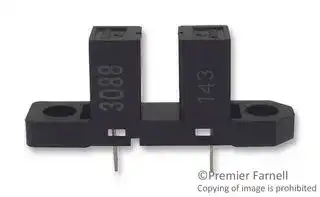
EESX4088
Transmissive Photo Interrupter, Photo / Optical IC, Through Hole, 3.4 mm, 0.5 mm, 50 mA, 4 V
⚠️ Reference pricing provided. In case of supply shortages, we will connect you with our trusted procurement partners to ensure your project's continuity.
- Manufacturer: OMRON ELECTRONIC COMPONENTS
- Product type: Transmissive Photo Interrupters
- Gap Width: 3.4mm
- Product Range: EE-SX4088 Series
- Sensor Output: Photo / Optical IC
- Aperture Width: 0.5mm
- Forward Voltage: 1.2V
- Sensor Mounting: Through Hole
- Forward Current If: 50mA
- Reverse Voltage Vr: 4V
| Delivery and price | |
|---|---|
| Units per pack | 50 |
| Price | 2.93 € |
| Current stock | 10+ |
| Lead time | 7 days |
Datasheet

## **Photomicrosensor (Transmissive) EE-SX3088/-SX4088**

**Be sure to read** _**Precautions**_ **on page 25.**

## ■ **Dimensions**

**Note:** All units are in millimeters unless otherwise indicated.

**==> picture [247 x 317] intentionally omitted <==**

**----- Start of picture text -----**<br>
25±0.2<br>Two, R1 19±0.15<br>- LATA + FESS -5+02 640.2<br>Two, 3.2±0.2 dia. holes Four, C0.3 Two, C2<br>12.8402<br>3.4402<br>0.5 rate ±0.1 0.5 t ±0.1<br>Optical axis<br>8.4±0.1 J | __ 472402 68401<br>3204 i Four, 0.25 _al es es<br>3.5±0.4 (1.28) (1.25) I,| Four, 0.5 LL gies<br>Cross section BB k | (9.2) Cross section AA ,<br>(e)<br>Internal Circuit<br>A G<br>K O © V<br>O<br>Unless otherwise specified, the<br>A O teahic O; G tolerances are as shown below.<br>Terminal No.          Name Dimensions           Tolerance<br>A     Anode 3 mm max. ±0.3<br>K     Cathode<br>3 < mm ≤ 6 ±0.375<br>V     Power supply 6 < mm ≤ 10 ±0.45<br>(Vcc)<br>10 < mm ≤ 18 ±0.55<br>O     Output (OUT)<br>G     Ground (GND) 18 < mm ≤ 30 ±0.65<br>**----- End of picture text -----**<br>


## ■ **Features**

- Incorporates an IC chip with a built-in detector element and amplifier.

- A wide supply voltage range: 4.5 to 16 VDC

- Directly connects with C-MOS and TTL.

- High resolution with a 0.5-mm-wide sensing aperture.

- Dark ON model (EE-SX3088)

- Light ON model (EE-SX4088)

- OMRON’s XK8-series Connectors can be connected to the lead wires without a PCB. Contact your OMRON representative for information on obtaining XK8-series Connectors.

## ■ **Absolute Maximum Ratings (Ta = 25** ° **C)**

|**Item**|**Item**|**Symbol**|**Rated value**|
|---|---|---|---|
|**Emitter**|**Forward current**|IF|50 mA<br>(see note 1)|
||**Reverse voltage**|VR|4 V|
|**Detector**|**Power supply volt-**<br>**age**|VCC|16 V|
||**Output voltage**|VOUT|28 V|
||**Output current**|IOUT|16 mA|
||**Permissible output**<br>**dissipation**|POUT|250 mW (see<br>note 1)|
|**Ambient tem-**<br>**perature**|**dissipation**<br>**Operating**|Topr|note 1)<br>–40°C to 75°C|
||**Storage**|Tstg|–40°C to 85°C|
|**Soldering temperature**||Tsol|260°C<br>(see note 2)|


- **Note: 1.** Refer to the temperature rating chart if the ambient temperature exceeds 25°C.

   **2.** Complete soldering within 10 seconds.

■ **Electrical and Optical Characteristics (Ta = 25** ° **C)**

|**Item**<br>~~Ge~~|**Item**<br>~~Ge~~|**Symbol**<br>~~Ge~~|**Value**<br>~~Ge~~|**Condition**<br>~~Ge~~|
|---|---|---|---|---|
|**Emitter**<br>**Forward voltage**<br>**Reverse current**<br>**Peak emission wave-**<br>**len**<br>~~Ge~~<br>~~eG~~|**Forward voltage**<br>~~Ge~~|VF<br>~~Ge ~~|1.2 V typ., 1.5 V max.<br> ~~GO~~|IF= 20 mA<br>~~GO~~|
||**Reverse current**<br>~~eG~~|IR<br>~~eG ~~|0.01μA typ., 10μA max.<br> ~~GO~~|VR= 4 V<br>~~GO~~|
||**Peak emission wave-**<br>**length**|λP|940 nm|IF= 20 mA|
|**Detector**<br>**Low-level output volt-**<br>**age**<br>**High-level output volt-**<br>**age**<br>**Current consumption**<br>**Peak spectral sensitivi-**<br>**t**<br>~~Se~~|**Low-level output volt-**<br>**age**<br>~~Se~~|VOL<br>~~Se~~|0.12 V typ., 0.4 V max.<br>~~Se~~|VCC= 4.5 to 16 V, IOL= 16 mA, IF= 0 mA (EE-SX3088),<br>IF= 5 mA (EE-SX4088)<br>~~Se~~|
||**High-level output volt-**<br>**age**<br>~~Se~~|VOH<br>~~Se~~|15 V min.<br>~~Se~~|VCC= 16 V, RL= 1 kΩ, IF= 5 mA (EE-SX3088),<br>IF= 0 mA (EE-SX4088)<br>~~Se~~|
||**Current consumption**<br>~~Se~~|ICC<br>~~Se~~|3.2 mA typ., 10 mA max.<br>~~Se~~|VCC= 16 V<br>~~Se~~|
||**Peak spectral sensitivi-**<br>**ty wavelength**<br>~~Se~~|λP<br>~~Se~~|870 nm<br>~~Se~~|VCC= 4.5 to 16 V<br>~~Se~~|
|**LED current when output is OFF**<br>~~pO~~||IFT<br>~~GG~~|2 mA typ., 5 mA max.<br>~~GG~~|VCC= 4.5 to 16 V<br>~~GG~~|
|**LED current when output is ON**<br>~~pO~~<br>~~De~~|||||
|**Hysteresis**<br>~~De~~<br>~~DR~~||ΔH<br>~~GG~~<br>~~Qe~~|15% typ.<br>~~GG~~|VCC= 4.5 to 16 V (see note 1)<br>~~GG~~|
|**Response frequency**<br>~~De ~~<br>~~DR~~||f<br> ~~GG~~<br>~~Qe~~|3kHz min.<br>~~GG~~|VCC= 4.5 to 16 V, IF= 15 mA, IOL= 16 mA (see note 2)<br>~~GG~~|
|**Response delay time**<br>~~DR~~<br>~~DG~~||tPLH(tPHL)<br>~~Qe~~<br>~~DG~~|3μs typ.<br>~~DG~~|VCC= 4.5 to 16 V, IF= 15 mA, IOL= 16 mA (see note 3)<br>~~DG~~|
|**Response delay time**<br>~~Ge~~||tPHL(tPLH)<br>~~Ge ~~|20μs typ.<br> ~~GG~~|VCC= 4.5 to 16 V, IF= 15 mA, IOL= 16 mA (see note 3)<br>~~GG~~|


**EE-SX3088/-SX4088** Photomicrosensor (Transmissive)

124

- **Note:** 1. Hysteresis denotes the difference in forward LED current value, expressed in percentage, calculated from the respective forward LED currents when the photo IC in turned from ON to OFF and when the photo IC in turned from OFF to ON.

   2. The value of the response frequency is measured by rotating the disk as shown below.

**==> picture [173 x 29] intentionally omitted <==**

**----- Start of picture text -----**<br>
2.1 mm<br>41a<br>0.5 mm Disk<br>an 0.5 mm<br>**----- End of picture text -----**<br>


3. The following illustrations show the definition of response delay time. The value in the parentheses applies to the EESX4088.

**==> picture [189 x 58] intentionally omitted <==**

**----- Start of picture text -----**<br>
Input —»t 0 OutputInput<br>Output —~t 0<br>tein teu. teHL<br>EE-SX3088 EE-SX4088<br>**----- End of picture text -----**<br>


## ■ **Engineering Data**

**Note:** The values in the parentheses apply to the EE-SX4088.

## **Forward Current vs. Collector Dissipation Temperature Rating**

## **Forward Current vs. Forward LED Current vs. Supply Voltage Voltage Characteristics (Typical) (Typical)**

**==> picture [9 x 138] intentionally omitted <==**

**----- Start of picture text -----**<br>
 (mW)<br>C<br>Output allowable dissipation P<br>**----- End of picture text -----**<br>


**==> picture [305 x 464] intentionally omitted <==**

**----- Start of picture text -----**<br>
Ta = 25°C<br>50 Ta = −30°C−30°C30°C°CC 6 I RL aa:  = 1 k Iez R. vee Ω<br>40** Ta = 25Ta = 70°°CCTa = 70°°CC°°CC°CCCCC /N | EES IFT OFF (IFT ON)FT OFF (IFT ON) OFF (IFT ON)FT ON) ON) ——||<br>IFT ON (IFT OFF)FT ON (IFT OFF) ON (IFT OFF)FT OFF) OFF)<br>°o 02 04 06 08 d11 y1212 14 |1616 18 0 0PPE2PPE22 4 6 8 10 12 4 «16<br>Forward voltage VF (V)F (V) (V) Supply voltage VCC (V)CC (V) (V)<br>Low-level Output Voltage vs.  Low-level Output Voltage vs. Am-<br>Output Current (Typical) bient Temperature Characteristics<br>(Typical)<br>nePott=AeeaSeaSSSeS ASeSAPott=AeeaSSeS ASeSAaSSSeS ASeSA ASeSASeSASA eeeses ee aesos a aesos a aos a a a a a Ta = 25VIFCC= 0 mA (15 mA)  = 5 V °CVIFCC= 0 mA (15 mA)  = 5 V °CIFCC= 0 mA (15 mA)  = 5 V °CFCC= 0 mA (15 mA)  = 5 V °CCC= 0 mA (15 mA)  = 5 V °C= 0 mA (15 mA)  = 5 V °C = 5 V °C°CC maniNO 018ote02ote02on042042 ld IcoJewR.JewR.ourVer BeenVer Been Beena ourVer BeenVer Been Beena V IFCC = 0 mA (15 mA) = 5 V IFCC = 0 mA (15 mA) = 5 VFCC = 0 mA (15 mA) = 5 VCC = 0 mA (15 mA) = 5 V = 0 mA (15 mA) = 5 V = 5 V<br>otnePott=AeeaSeaSSSeS ASeSAPott=AeeaSSeS ASeSAaSSSeS ASeSA ASeSASeSASA SeaSSSeS ASeSAPott=AeeaSSeS ASeSAaSSSeS ASeSA ASeSASeSASA ATTGS>GSTTGS>GSGS>GS>GSGS > ~OSceTTTNSaay GS HaOSceTTTNSaay GS HaceTTTNSaay GS HaTTTNSaay GS HaNSaay GS Haaay GS Ha GS Ha Ha NO | on042042 BRRRSREREEE IOL = 16 mAOL = 16 mA = 16 mA a at AdP AdPP<br>Poe |_| HT] | | |<br>a a 01 |}<br>zy eG|| LEEopop te tT]TTTT<br>SSaa Ss... eae |<br>rePa tyee tyee ee tyee ee ve 0.04 |} 4+} [[te]] ———<br>PotPa tyrePa tyee tyee wTourourve |] 0020.04 ||} IOL = 5 mAOL = 5 mA = 5 mA PEELE———<br>0.001 | TTT mal 0 Lt | Baaen<br>1 10 100 -50 -40 -30 -20-10 0 10 20 30 40 50 60 70 80<br>Output current IC (mA)C (mA) (mA) Ambient temperature Ta (°C)°C)C)<br>Response Delay Time vs. Forward  Repeat Sensing Position<br>Current (Typical) Characteristics (Typical)<br>VCC = 5 V CC = 5 V  = 5 V  Ta = 25°C °C C<br>... Ta = 25RL = 330 °C ΩRL = 330 °C ΩL = 330 °C Ω = 330 °C Ω°C ΩC ΩΩ Pi|| td VIFCC = 15 mA = 5 V IFCC = 15 mA = 5 V FCC = 15 mA = 5 V CC = 15 mA = 5 V  = 15 mA = 5 V  = 5 V<br>25ao V(EE-SX3V(EE-SX4OUTOUT(EE-SX3V(EE-SX4OUTOUTV(EE-SX4OUTOUT(EE-SX4OUTOUT@@@@))@@))))) @@@@))@@))))) +—fe)eae feEs—fe)eae feEsfe)eae feEseae feEs feEs (OFF)ON n = repeat 20 timesRL = 330 RL = 330 L = 330  = 330 Ω i d1 = 0.01 mmΩ1 = 0.01 mmΩ = 0.01 mmΩ<br>2015PIVUne1re‘tPLH)15PIVUne1re‘tPLH)PIVUne1re‘tPLH)Une1re‘tPLH)1re‘tPLH)re‘tPLH)‘tPLH) lk kee RLVeeVee ke lec _—HyHlHyHlHl 7 aa6a66 Center of optical axis —-0-+||<br>10 \ freer‘OUT ie"teVeeuF"teVeeuFteVeeuFVeeuFuF HAis |‘<br>5 IN ei ‘GNO roe > yHyHy<br>5Py)Py) ——MEETMEET o rentTJ4ntTJ4tTJ4J44 |<br>ce 5 10 15 20 25 30 35 40. 04 03 02 01 0 01 02 03 04 05 06<br>Forward current IF (mA)F (mA) (mA) Distance d (mm)<br> (mA)<br>F  (mA)<br>FT<br>LED current  I<br>Forward current  I<br> (V)<br>OL<br>Low level output voltage  V<br>s)<br>μ<br> (<br>PLH<br>, t<br>PHL<br>Output transistor<br>Response delay time t<br>**----- End of picture text -----**<br>


**==> picture [474 x 453] intentionally omitted <==**

**----- Start of picture text -----**<br>
50 260 50 6 I Iez vee<br>Ta = −30°C−30°C30°C°CC aa: R.<br>40 1200 Ta = 25Ta = 70°°CCTa = 70°°CC°°CC°CCCCC N | IFT OFF (IFT ON)FT OFF (IFT ON) OFF (IFT ON)FT ON) ON) ——||<br>. tH" 40** /N EES<br>IFT ON (IFT OFF)FT ON (IFT OFF) ON (IFT OFF)FT OFF) OFF)<br>vy) 20. °~«20 2. +40 «60 BO 700 °o 02 04 06 08 d11 y1212 14 |1616 18 0 0PPE2PPE22 4 6 8 10 12 4<br>Ambient temperature Ta (°C) Forward voltage VF (V)F (V) (V) Supply voltage VCC (V)CC (V) (V)<br>LED Current vs. Ambient Temper- Low-level Output Voltage vs.  Low-level Output Voltage vs. Am-<br>ature Characteristics (Typical) Output Current (Typical) bient Temperature Characteristics<br>(Typical)<br>7 02<br>6 VRCCL = 330  = 5 VΩ =AeeaAeeaeeaa eeeses ee aesos a aesos a aos a a a a a Ta = 25VIFCC= 0 mA (15 mA)  = 5 V °CVIFCC= 0 mA (15 mA)  = 5 V °CIFCC= 0 mA (15 mA)  = 5 V °CFCC= 0 mA (15 mA)  = 5 V °CCC= 0 mA (15 mA)  = 5 V °C= 0 mA (15 mA)  = 5 V °C = 5 V °C°CC ld R. V IFCC = 0 mA (15 mA) = 5 V IFCC = 0 mA (15 mA) = 5 VFCC = 0 mA (15 mA) = 5 VCC = 0 mA (15 mA) = 5 V = 0 mA (15 mA) = 5 V = 5 V<br>s4 Ss IFT OFF (IFT ON) “TT otnePott=AeeaSeaSSSeS ASeSAPott=AeeaSSeS ASeSAaSSSeS ASeSA ASeSASeSASA ATTGS>GSTTGS>GSGS>GS>GSGS > ~OSceTTTNSaay GS HaOSceTTTNSaay GS HaceTTTNSaay GS HaTTTNSaay GS HaNSaay GS Haaay GS Ha GS Ha Ha maniNO | 018ote02ote02on042042 BRRRSREREEE IOL = 16 mAOL = 16 mA = 16 mA IcoJewR.JewR.ourVer BeenVer Been Beena at AdP AdPP<br>ee ae i Poe |_| HT] | | |<br>: DLO a a 01 |}<br>2Py IFT  yy  ON (IFT OFF) Lt zy eG|| LEEopop te tT]TTTT<br>——cs veo SSaa Ss... eae |<br>1 voraour PotPa tyrePa tyee tyee wTourourve |] 0020.04 ||} 4+} [[te]] IOL = 5 mAOL = 5 mA = 5 mA PEELE———<br>° “0 0.001 | TTT mal 0 Lt | Baaen<br>-60 -40 -20 ° 20 40 60 80 1 10 100 -50 -40 -30 -20-10 0 10 20 30 40 50 60 70 80<br>Ambient temperature Ta (°C) Output current IC (mA)C (mA) (mA) Ambient temperature Ta (°C)°C)C)<br>Current Consumption vs. Supply  Response Delay Time vs. Forward  Repeat Sensing Position<br>Voltage (Typical) Current (Typical) Characteristics (Typical)<br>Ta = 25°C VCC = 5 V CC = 5 V  = 5 V  Ta = 25°C °C C<br>wt 1td  IF = 0 mA (15 mA) ... Ta = 25RL = 330 °C ΩRL = 330 °C ΩL = 330 °C Ω = 330 °C Ω°C ΩC ΩΩ Pi|| td VIFCC = 15 mA = 5 V IFCC = 15 mA = 5 V FCC = 15 mA = 5 V CC = 15 mA = 5 V  = 15 mA = 5 V  = 5 V<br>n = repeat 20 timesRL = 330 RL = 330 L = 330  = 330 Ω<br>= ao OUTOUTOUT Es ON<br>os ptt | | Per 25ao V(EE-SX3V(EE-SX4OUTOUT(EE-SX3V(EE-SX4OUTOUTV(EE-SX4OUTOUT(EE-SX4OUTOUT@@@@))@@))))) +—fe)eae feEs—fe)eae feEsfe)eae feEseae feEs feEs (OFF)ON i d1 = 0.01 mmΩ1 = 0.01 mmΩ = 0.01 mmΩ<br>2eet. | 7 Center of optical axis<br>16 PF itt tT 2015PIVUne1re‘tPLH)15PIVUne1re‘tPLH)PIVUne1re‘tPLH)Une1re‘tPLH)1re‘tPLH)re‘tPLH)‘tPLH) lk kee aa6a66 —-0-+||<br>RLVeeVee ke lec _—HyHlHyHlHl<br>1 Ie Ice ‘OUT Aisis ‘<br>~t 10 \ freer‘OUT ie"teVeeuF"teVeeuFteVeeuFVeeuFuF HAis |‘<br>05 WeUT 5 IN ei ‘GNO roe > yHyHy<br>3 fe" 5Py)Py) ——MEETMEET o rentTJ4ntTJ4tTJ4J44 |<br>i 2 4 6 8 0 12 14 16 ce 5 10 15 20 25 30 35 40. 04 03 02 01 0 01 02 03 04 05 06<br>Supply voltage VCC (V) Forward current IF (mA)F (mA) (mA)<br>C<br> (mA) F  (mA)<br>F FT<br>LED current  I<br>Forward current  I<br>Forward current  I<br>Output allowable dissipation P<br> (V)  (V)<br>OL OL<br> (mA)<br>FT<br>LED current  I<br>Low level output voltage  V Low level output voltage  V<br>s)<br>μ<br> (<br>PLH<br>, t<br>PHL<br>Output transistor<br>Current consumption  Icc (mA)<br>Response delay time t<br>**----- End of picture text -----**<br>


**Low-level Output Voltage vs. Ambient Temperature Characteristics (Typical)**

**EE-SX3088/-SX4088** Photomicrosensor (Transmissive)

125
Updated at February 9, 2023
About Novapart
Novapart is a B2B electronic component broker specialising in stock shortages and cost reduction. We source hard-to-find parts and identify compliant alternatives across a catalogue of 410,000+ components from 500+ manufacturers.
Learn more →Stock Shortage Specialist
When a component is unavailable, discontinued or has an unacceptable lead time, we tap into our network of vetted European and Asian distributors to source what you need — without compromising on quality or traceability.
Request a quote →Compliant Alternatives
We identify pin-to-pin, electrically equivalent substitutes that meet the same certifications (RoHS, AEC-Q100, REACH) as your original specification — validated against datasheets, not just part numbers. Often at a lower cost.
BOM Analysis service →