
Image not available
Illustrative purposes only

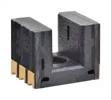
EE-SX4320
Transmissive Photo Interrupter, Photo / Optical IC, SMD, 2 mm, 0.3 mm, 25 mA, 5 V
⚠️ Reference pricing provided. In case of supply shortages, we will connect you with our trusted procurement partners to ensure your project's continuity.
- Manufacturer: OMRON ELECTRONIC COMPONENTS
- Product type: Transmissive Photo Interrupters
- Gap Width: 2mm
- Sensor Output: Photo / Optical IC
- Aperture Width: 0.3mm
- Forward Voltage: 1.2V
- Sensor Mounting: SMD
- Forward Current If: 25mA
- Reverse Voltage Vr: 5V
| Delivery and price | |
|---|---|
| Units per pack | 50 |
| Price | 2.04 € |
| Current stock | 1000+ |
| Lead time | 7 days |
Datasheet

**Photomicrosensor (Transmissive) EE-SX4320** ## **Ultra-Compact Slot / SMD Type (Slot width: 2 mm)** • PCB surface mounting type. • High resolution with a 0.3-mm-wide aperture. **Be sure to read** _**Safety Precautions**_ **on page 3.** ~~a0~~ ## **Ordering Information** |**Ordering Informationg Information Information**|| |---|---| |**Photomicrosensor**|| |**Appearance**<br>**Sensing**<br>**method**<br>**Connecting**<br>**method**<br>**Sensing distance**<br>**Aperture size (H× W)**<br>**(mm)**<br>**Output type**<br>**Model**<br>Transmissive<br>(slot type)<br>SMT<br>Emitter<br>1.4×1.4<br>Detector<br>1×0.3<br>Photo IC<br>**EE-SX4320**<br>4<br>5.1<br>4<br>4320<br>N561<br>**2 mm**(slot width)<br>~~eo~~|| |**Ratings, Characteristics and Exterior Specifications**|| |**Absolute Maximum Ratings(Ta = 25°C)**|**Electrical and Optical Characteristics (Ta = 25°C)**| |**Item**<br>**Symbol**<br>**Rated value**<br>**Unit**<br>**Emitter**|**Item**<br>**Symbol**<br>**Value**<br>**Unit**<br>**Condition**<br>**MIN.**<br>**TYP.**<br>**MAX.**<br>~~=~~| |*1.Refer to the temperature rating chart if the ambient temperature<br>exceeds 25°C.<br>*2.Complete soldering within 10 seconds for reflow soldering.<br>**Exterior Specifications**<br>**Forward current**<br>IF<br>25 *1<br>mA<br>**Reverse voltage**<br>VR<br>5<br>V<br>**Detector**<br>**Power supply voltage**<br>VCC<br>9<br>V<br>**Output voltage**<br>VOUT<br>17<br>V<br>**Output current**<br>IOUT<br>8<br>mA<br>**Permissible output**<br>**dissipation**<br>POUT<br>80*1<br>mW<br>**Operating temperature**<br>Topr<br>-30to +85 *1<br>°C<br>**Storage temperature**<br>Tstg<br>-40to +90 *1<br>°C<br>**Reflow soldering**<br>**temperature**<br>Tsol<br>255 *2<br>°C<br>**Connecting method**<br>**Weight (g)**<br>**Material**<br>**Case**<br>SMT<br>0.1<br>PPS<br>~~2~~|*1.Hysteresis denotes the difference in forward LED current value,<br>**Emitter**<br>**Forward**<br>**voltage**<br>VF<br>---<br>1.2<br>1.4<br>V<br>IF= 20 mA<br>**Reverse**<br>**current**<br>IR<br>---<br>0.01<br>10<br>A<br>VR= 5 V<br>**Peak**<br>**emission**<br>**wavelength**<br>P<br>---<br>940<br>---<br>nm<br>IF= 20 mA<br>**Detector**<br>**Power supply**<br>**voltage**<br>VCC<br>2.2<br>---<br>7<br>V<br>---<br>**Low-level**<br>**output**<br>**voltage**<br>VOL<br>---<br>0.12<br>0.4<br>V<br>VCC= 2.2 to 7 V,<br>IF= 7 mA,<br>IOL= 8 mA<br>**High-level**<br>**output**<br>**voltage**<br>IOH<br>---<br>---<br>10<br>A<br>VCC=2.2 to 7 V,<br>IF=0 mA,<br>VOH=17 V<br>**Current**<br>**consumption**<br>ICC<br>---<br>2.8<br>4<br>mA<br>VCC= 7 V<br>**Peak spectral**<br>**sensitivity**<br>**wavelength**<br>P<br>---<br>870<br>---<br>nm<br>VCC=2.2to7 V<br>**LED current when**<br>**output is OFF**<br>IFT<br>---<br>---<br>3.5<br>mA<br>VCC=2.2to7 V<br>**Hysteresis**<br>H<br>---<br>21<br>---<br>%<br>VCC=2.2to7 V <br>*1<br>**Response**<br>**frequency**<br>f<br>3<br>---<br>---<br>kHz<br>VCC=2.2 to 7 V,<br>IF=5 mA,<br>IOL=8 mA*2<br>**Response delay**<br>**time**<br>tPLH<br>---<br>8<br>---<br>s<br>VCC=2.2 to 7 V,<br>IF=5 mA,<br>IOL=8 mA*3<br>tPHL<br>---<br>20<br>---<br>s<br>VCC=2.2 to 7 V,<br>IF=5 mA,<br>IOL=8 mA*3<br>~~—~~<br>~~|~~<br>~~|~~<br>~~|~~<br>~~ft |~~<br>~~—~~<br>~~|~~<br>~~| tt i~~<br>~~FP] itt~~<br>~~tT~~<br>~~TT~~<br>~~| El~~<br>~~| Tid~~<br>~~tT~~<br>~~TT~~<br>~~|~~<br>~~tt~~<br>~~P|~~<br>~~| tf~~<br>~~Pt~~<br>~~tT |~~<br>~~Pt~~<br>~~i|~~<br>~~Ft td~~| - *1. Hysteresis denotes the difference in forward LED current value, expressed in percentage, calculated from the respective forward LED currents when the photo IC in turned from ON to OFF and when the photo IC in turned from OFF to ON. **1** OmRON ~~a~~ **EE-SX4320** *2. The value of the response frequency is measured by rotating the disk as shown below. The value of the response frequency is measured by rotating the *3. The following illustrations show the definition of response delay disk as shown below. time. Disk Input 0 t Output 0 t tPHL tPLH 0.5 mm 0.5 mm ~~Ge[A]~~[m] ~~Le~~ ee ## **Engineering Data (Reference value)** **Fig 1. Forward Current vs. Collector Dissipation Temperature Rating** **Fig 2. Forward Current vs. Forward Voltage Characteristics (Typical)** **Fig 3. LED Current vs. Supply Voltage (Typical)** **==> picture [492 x 517] intentionally omitted <==** **----- Start of picture text -----**<br> 60 120 30 2<br>Ta = 25°C<br>RL = 4.7 kΩ<br>50 TOO) 100 25 )§=69otooo<br>1.5<br>POUT Ta = -30°C<br>40 80 20<br>IFT ON<br>PEPEEPE) Geer ge HEL<br>30 PTENCEE) 60 = Eerie 15 Ta = +25°C 1 LL<br>IF<br>20 40 10 Ta = +70°C IFT OFF<br>0.5 IF ICC<br>VCC<br>10 20 5 RLOUT<br>VOUT<br>GND<br>0-40 CeePP -20 0 20 40 NG 60 80 100 ) 0 = Gece 0 0 0.2 0.4 0.6 0.8 1 1.2 1.4 1.6 0 0 LLL 1 2 3 4 5 6 7 8 9 10<br>Ambient temperature Ta (ºC) Forward voltage VF (V) Supply voltage VCC (V)<br>Fig 4.LED Current vs. Ambient LED Current vs. Ambient Fig 5. Low-level Output Voltage vs. Fig 6. Low-level Output Voltage vs. Low-level Output Voltage vs.<br>Temperature Characteristics (Typical) Output Current (Typical) Ambient Temperature Characteristics<br>(Typical)<br>2 1 0.12<br>Vcc = 5 V Ta = 25ºC IF ICC VCC VIF CC = 7 mA= 5 V<br>RL = 4.7 kΩ VIOLCC = 8 mA = 5 V 0.1 RLOUT<br>IF = 7 mA VOUT<br>1.5 GND<br>ee 0.1 aoa=== 0.08 et<br>IFT ON IOL = 8 mA<br>1 0.06<br>IFT OFF 0.01 0.04<br>0.5 IF ICC VCC V CC IOL = 0.5 mA<br>RLOUT IOUTOUT 0.02<br>VOUT<br>GND GND<br>0-40 (ie -20 0 20 40 60 80 100 | 0.001 1 ESS 10 | 0−40 eee −20 0 20 40 60 80 100<br>Ambient temperature Ta (ºC) Output current IC (mA) Ambient temperature Ta (°C)<br>Fig 7. Current Consumption vs. Supply Current Consumption vs. Supply Fig 8. Response Delay Time vs. Response Delay Time vs. Fig 9. Repeat Sensing Position<br>Voltage (Typical) Forward Current (Typical) Characteristics (Typical)<br>4 40<br>3.5 Pt | | Ta = 25ºC IF = 0 mA 35 IF ICCRLVOUTCC V R TaCC L = = = 4.7 k 255 VºC Ω (Center of optical axis) cos d t Ta = 25ºCIRVFCCL = 5 mA = 4.7 k = 5 VΩ<br>3 30 VOUTGND n = repeat 20 times<br>2.5 25 ON<br>po RE tPLH OFF Light f ae |<br>baffle<br>2 Pf | dee 20 | | | FT |<br>INPUT IF d1 = 0.005 mm<br>1.5 15 t<br>OUTPUT t IF ICC VCC<br>0.51 IF ICC VROUTLV OUT CC 105 tPHL tPHL tPLH VROUTLOUTGND<br>GND<br>00 eH 1 2 Supply voltage V3 4 5CC (V)6 7 | 8 00 ES] 5 Forward current I10 15 F (mA)20 25 30 (ON)OFF −0.1 0 Distance d (mm) L 0.1 LL 0.2 0.3<br> (mW)<br>OUT<br> (mA)F (mA)F (mA)FT<br>Forward current I LED current I<br>Forward current I<br>Output allowable dissipation P<br> (V) (V)<br>OL OL<br> (mA)<br>FT<br>LED current I<br>Low level output voltage V Low level output voltage V<br> (µs)<br>PLH<br> (mA) , t<br>CC PHL (<br>)<br>Current consumption I Response delay time t Output transistor<br>**----- End of picture text -----**<br> **Fig 4.LED Current vs. Ambient LED Current vs. Ambient Temperature Characteristics (Typical)** **Fig 6. Low-level Output Voltage vs. Low-level Output Voltage vs. Ambient Temperature Characteristics (Typical)** **Fig 7. Current Consumption vs. Supply Current Consumption vs. Supply Fig 8. Response Delay Time vs. Response Delay Time vs. Voltage (Typical) Forward Current (Typical)** **2** **EE-SX4320** ## **Safety Precautions** ## **To ensure safe operation, be sure to read and follow the Instruction Manual provided with the Sensor.** ## **CAUTION** **This product is not designed or rated for ensuring safety of persons either directly or indirectly. Do not use it for such purposes.** ## **Precautions for Safe Use** **Do not use the product with a voltage or current that exceeds the rated range.** **Precautions for Correct Use** **Do not use the product in atmospheres or environments that exceed product ratings. This product is for surface mounting. Refer to Soldering Information, Storage and Baking for details.** **Dispose of this product as industrial waste.** Applying a voltage or current that is higher than the rated range may result in explosion or fire. **Do not miswire such as the polarity of the power** ## **supply voltage.** Otherwise the product may be damaged or it may burn. **Do not short-circuit the load.** Otherwise explosion or burning may occur. **This product does not resist water. Do not use the product in places where water or oil may be sprayed onto the product.** ## **Dimensions and Internal Circuit** **(Unit: mm)** ## **Photomicrosensor** **==> picture [69 x 91] intentionally omitted <==** **----- Start of picture text -----**<br> EE-SX4320<br>™<br>Aperture size (H x W)<br>**----- End of picture text -----**<br> **==> picture [485 x 391] intentionally omitted <==** **----- Start of picture text -----**<br> Ejector pin, gate mark, or flat surface<br>2.0 mm dia. or 0.5 mm recess (MAX)<br>Emitter side (1) (6) Detector side<br>(2) (5)<br>nea<br>_ (3) l =pmaul (4)<br> 5.1<br>Aperture size (H x W)<br>Emitter 1.4×1.4 Detector 1×0.3 Terminals are exposedin the end face of the board Terminals are exposedin the end face of the board Marking(upper: model, lower: lot No.)<br>Optical axis 2 ±0.2 1.55 0.3 ±0.15<br> 1.4 A B<br>Ns<br>cm | im Ns<br>: LIL]<br> R0.3 R0.3<br>Mi g ) IP<br>A B<br>Cross section view B-B 1 1 1 (0.4) (0.4) 1 1 1 Cross section view A-A<br>(Emitter side) anja 2.8 i ! anjaaint 2.8 (Detector side)<br>Internal circuit<br>(1) (6)<br>(5)<br>(2)<br>(3) <n , (4) Pet! 2 3.1 2<br>Terminal No. Name<br>(1) Anode<br>(2)(3) Cathode<br>(4) ground<br>Power supply<br>(5)<br>voltage<br>Unless otherwise specified, the tolerances are ±0.2 mm.<br>(6) Output<br>(6xC0.2)<br> 4<br> 1 1 1<br> 2.8<br> 1.4 4 1<br> 1 1<br> 1<br> 1<br> 1<br> 0.4 0.4<br>**----- End of picture text -----**<br> **==> picture [175 x 8] intentionally omitted <==** **----- Start of picture text -----**<br> Unless otherwise specified, the tolerances are ±0.2 mm.<br>**----- End of picture text -----**<br> **3** **EE-SX4320** **Tape and Reel** ## **Reel (Unit: mm)** **==> picture [252 x 157] intentionally omitted <==** **----- Start of picture text -----**<br> 21 [±0.8 dia. ]<br>2 [±0.5]<br>13 [±0.2 dia.]<br>80 [±1dia.]<br>330 [±2 dia.]<br>a PHOTO MICROSENSOR Product name 1<br>Lot number Quantity<br>Country of origin<br>—| H fb<br>Ho<br>W1 = 13.5 [±1]<br>W2 = 17.5 [±1] W1<br>a7<br>W2<br>**----- End of picture text -----**<br> **Tape (Unit: mm)** **==> picture [182 x 205] intentionally omitted <==** **----- Start of picture text -----**<br> 1.5 dia.<br>77<br>G K<br>V<br>O ial A ><br>Tape Pull-out direction<br>Note: Direction of product packing is upper figure.<br>**----- End of picture text -----**<br> **4** omron ~~a~~ **EE-SX4320** ## **Soldering Information** ## **Reflow soldering: Temperature profile** The reflow soldering can be implemented in two times complying with the following diagram. All the temperatures in the product must be within the diagram. **==> picture [227 x 127] intentionally omitted <==** **----- Start of picture text -----**<br> 260°C max.<br>255°C<br>1 to 4°C/s<br>230°C<br>10 sec max. 1 to 4°C/sec<br>150 to 180°C max.<br>40 sec max.<br>1 to 4°C/s<br>120 sec max.<br>Temperature (°C)<br>**----- End of picture text -----**<br> ## **Manual soldering** The manual soldering should not be applied to the products, otherwise the housing may be deformed and/or the Au plating may be peeled off by heat. ## **Other notes** The use of infrared lamp causes the temperature at the resin to rise particularly too high. All the temperatures in the product must be within the above diagram. Do not immerse the resin part into the solder. Even if within the above temperature diagram, there is a possibility that the gold wire in the products is broken in case that the deformation of PC board gives stress to the products. Please confirm the conditions (including material and method of flux and cleaning) of the reflow soldering fully by actual solder reflow machine prior to the mass production use. **==> picture [20 x 6] intentionally omitted <==** **----- Start of picture text -----**<br> Time (s)<br>**----- End of picture text -----**<br> ## **Storage** ## **Storage conditions** To protect the product from the effects of humidity until the package is opened, dry-box storage is recommended. If this is not possible, store the product under the following conditions: - Temperature: 10 to 30 °C Humidity: 60% RH max. ## **Treatment after open** **1.** Reflow soldering must be done within 48 hours stored at the conditions of humidity 60% RH or less and temperature 10 to 30°C. **2.** If the product must be stored after it is unpacked, store it in a dry box or reseal it in a moisture-proof package with desiccant at a temperature of 10 to 30°C and a humidity of 60% RH or less. Even then, mount the product within one week. ## **Baking** In case that it could not carry out the above treatment, it is able to mount by the following baking treatment. However baking treatment shall be limited only 1 time. - Recommended conditions: 60°C for 24 to 48 hours (reeled one) 100°C for 8 to 24 hours (loose one) **5** - Application examples provided in this document are for reference only. In actual applications, confirm equipment functions and safety before using the product. - Consult your OMRON representative before using the product under conditions which are not described in the manual or applying the product to nuclear control systems, railroad systems, aviation systems, vehicles, combustion systems, medical equipment, amusement machines, safety equipment, and other systems or equipment that may have a serious influence on lives and property if used improperly. Make sure that the ratings and performance characteristics of the product provide a margin of safety for the system or equipment, and be sure to provide the system or equipment with double safety mechanisms. **Note: Do not use this document to operate the Unit.** **OMRON Corporation Electronic and Mechanical Components Company** **Contact: www.omron.com/ecb** **Cat. No. E458-E1-03** 1116(0816)(O)
Updated at February 9, 2023
About Novapart
Novapart is a B2B electronic component broker specialising in stock shortages and cost reduction. We source hard-to-find parts and identify compliant alternatives across a catalogue of 410,000+ components from 500+ manufacturers.
Learn more →Stock Shortage Specialist
When a component is unavailable, discontinued or has an unacceptable lead time, we tap into our network of vetted European and Asian distributors to source what you need — without compromising on quality or traceability.
Request a quote →Compliant Alternatives
We identify pin-to-pin, electrically equivalent substitutes that meet the same certifications (RoHS, AEC-Q100, REACH) as your original specification — validated against datasheets, not just part numbers. Often at a lower cost.
BOM Analysis service →