
Image not available
Illustrative purposes only

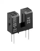
EE-SX199
Transmissive Photo Interrupter, Phototransistor, Through Hole, 3 mm, 0.5 mm, 50 mA, 4 V
⚠️ Reference pricing provided. In case of supply shortages, we will connect you with our trusted procurement partners to ensure your project's continuity.
- Manufacturer: OMRON ELECTRONIC COMPONENTS
- Product type: Transmissive Photo Interrupters
- Gap Width: 3mm
- Sensor Output: Phototransistor
- Aperture Width: 0.5mm
- Forward Voltage: 1.2V
- Sensor Mounting: Through Hole
- Forward Current If: 50mA
- Reverse Voltage Vr: 4V
| Delivery and price | |
|---|---|
| Units per pack | 59 |
| Price | 1.69 € |
| Current stock | 10+ |
| Lead time | 30 days |
Datasheet

## **7Photomicrosensor (Transmissive) EE-SX199**

**Be sure to read** _**Precautions**_ **on page 25.**

## ■ **Dimensions**

**Note:** All units are in millimeters unless otherwise indicated.

## ■ **Features**

- General-purpose model with a 3-mm-wide slot.

- PCB mounting type.

**==> picture [250 x 313] intentionally omitted <==**

**----- Start of picture text -----**<br>
12.2±0.3<br>5±0.1<br>0.5±0.1 Four, C0.3 Two, C1±0.3<br>Optical axis<br>10±0.2<br>8.5±0.1<br>6.5±0.1<br>= ! |<br>6.2±0.5<br>i il<br>Four, 0.25±0.1 Four, 0.5±0.1<br>Cross section BB 2.5±0.1<br>Two, 0.7 [ 0] -0.1 dia. 9.2±0.3<br>Cross section AA<br>K C<br>4.3<br>A E<br>Internal Circuit<br>K C<br>A E<br>Terminal No.     Name<br>A     Anode<br>K     Cathode<br>Unless otherwise specified,<br>C     Collector<br>the tolerances are ±0.2 mm.<br>E     Emitter<br>**----- End of picture text -----**<br>


- High resolution with a 0.5-mm-wide aperture.

- With a positioning boss.

## ■ **Absolute Maximum Ratings (Ta = 25** ° **C)**

|**Item**|**Item**|**Symbol**|**Rated value**|
|---|---|---|---|
|**Emitter**|**Forward current**|IF|50 mA<br>(see note 1)|
||**Pulse forward cur-**<br>**rent**|IFP|1 A<br>(see note 2)|
||**Reverse voltage**|VR|4 V|
|**Detector**|**Collector–Emitter**<br>**voltage**|VCEO|30 V|
||**Emitter–Collector**<br>**voltage**|VECO|---|
||**Collector current**|IC|20 mA|
||**Collector dissipa-**<br>**tion**|PC|100 mW<br>(see note 1)|
|**Ambient tem-**<br>**perature**|**Operating**|Topr|–25°C to 85°C|
||**Storage**|Tstg|–40°C to<br>100°C|
|**Soldering temperature**||Tsol|260°C<br>(see note 3)|


- **Note: 1.** Refer to the temperature rating chart if the ambient temperature exceeds 25°C.

   **2.** The pulse width is 10 μs maximum with a frequency of 100 Hz.

   **3.** Complete soldering within 10 seconds.

## ■ **Electrical and Optical Characteristics (Ta = 25** ° **C)**

~~es~~ **Item** ~~eG~~ **Symbol Value Condition Emitter** ~~GQ~~ **Forward voltage** VF 1.2 V typ., 1.4 V max. IF = 30 mA **Reverse current** IR 0.01 μA typ., 10 μA max. VR = 4 V ~~eSGO~~ **Peak emission wavelength** λP 940 nm typ. ~~eee~~ IF = 20 mA **Detector** ~~RO~~ **Light current** IL 0.5 mA min., 14 mA max. IF = 20 mA, VCE = 5 V ~~sO~~ **Dark current** ID 2 nA typ., 200 nA max. VCE = 20 V, 0 lx ~~GO~~ **Leakage current** ILEAK ----- **Collector–Emitter saturated volt-** VCE (sat) 0.1 V typ., 0.4 V max. IF = 40 mA, IL = 0.5 mA **age Peak spectral sensitivity wave-** λP 850 nm typ. VCE = 10 V ~~SSSSs~~ **length** ~~Pe~~ **Rising time** tr 4 μs typ. VCC = 5 V, RL = 100 Ω, IL = 5 mA ~~GO~~ **Falling time** tf 4 μs typ. VCC = 5 V, RL = 100 Ω, IL = 5 mA

**EE-SX199** Photomicrosensor (Transmissive)

96

## ■ **Engineering Data**

**==> picture [486 x 347] intentionally omitted <==**

**----- Start of picture text -----**<br>
Forward Current vs. Collector  Forward Current vs. Forward  Light Current vs. Forward Current<br>Dissipation Temperature Rating Voltage Characteristics (Typical) Characteristics (Typical)<br>60 150 60 20 Ta = 25°C<br>IF VCE = 5 V<br>Pid | PITT ety Ty) HS Z<br>Ta = −30°C<br>PC Ta = 25°C<br>. ote EL EERE<br>Ta = 70°C<br>.LNA | | Hel | anne<br>\! . i) SOOT<br>20NL PP ) AREAL<br>PT TN 50 20 6HA<br>HEE-40  -20 0 20 40 60 80eee)= 100 0Le02 04 06 08 1 #12 Sel14 16 18 eeeCoA20anebs 10 20 30 40 50<br>Ambient temperature Ta (°C) Forward voltage VF (V) Forward current IF (mA)<br>Light Current vs. Collector − Emitter  Relative Light Current vs. Ambi- Dark Current vs. Ambient<br>Voltage Characteristics (Typical) ent Temperature Characteristics  Temperature Characteristics<br>(Typical) (Typical)<br>TO16|16|| Ta = 25°CC | °CC |TTLdPaTTLdPadPaa IFF = 50 mA |4|4|| 120110 IVFCE= 20 mA  = 5 V 10.000Fe)ene 0 VCElx ee  = 10 V eeee<br>IFF = 40 mA<br>(= ———eee ———eeeeee en See ———=====-------|<br>al IFF = 30 mA ea A a<br>1s = <aahwN soe oe<br>De e of eS<br>IFF = 20 mA — SS<br>IFF = 10 mA<br>Tsaeeeeeeeesaeeeeeeee TT 79TP a 2aS >SSsaaees<br>a a eT 85. ~«20OC~St*t*«atStC«SC<aS*C«iaSC*dO 0.001 Fae<br>Collector−Emitter voltage VCE (V)−Emitter voltage VCE (V)Emitter voltage VCE (V)CE (V) (V) Ambient temperature Ta (°C) Ambient temperature Ta (°C)<br> (mW)  (mA)<br> (mA) C F<br>F  (mA)<br>L<br>Forward current  I Light current  I<br>Forward current  I<br>Collector dissipation P<br> (%)<br>L<br> (mA)<br>L<br> (nA)<br>D<br>Light current  I<br>Dark current   I<br>Relative light current  I<br>**----- End of picture text -----**<br>


**==> picture [144 x 144] intentionally omitted <==**

**----- Start of picture text -----**<br>
Ta = 25°CC IFF = 50 mA<br>TO16|16|| | |TTLdPaTTLdPadPaa |4|4||<br>IFF = 40 mA<br>(= ———eee ———eeeeee en<br>al IFF = 30 mA<br>1s =<br>De e<br>IFF = 20 mA —<br>IFF = 10 mA<br>Tsaeeeeeeeesaeeeeeeee TT<br>a a eT<br>Collector−Emitter voltage VCE (V)−Emitter voltage VCE (V)Emitter voltage VCE (V)CE (V) (V)<br> (mA)<br>L<br>Light current  I<br>**----- End of picture text -----**<br>


**==> picture [497 x 293] intentionally omitted <==**

**----- Start of picture text -----**<br>
Response Time vs. Load Resist- Sensing Position Characteristics  Sensing Position Characteristics<br>ance Characteristics (Typical) (Typical) (Typical)<br>000Cn=eie Ta = 25VCC = 5 V °C tH ‘00120 VITa = 25FCE= 20 mA  = 10 V °C   100120 = Ta = 25IVFCE= 20 mA  = 10 V °C<br>(Center of<br>optical axis)<br>eS CS a A ne 0 ee) 80 80<br>d<br>i oe eT aa \ | | Pl 60 | | | iM | :<br>ook UE I LTT “Ne « il H il 9<br>Pee 2 Sea 40 | | | |)<br>cos © rill \ il<br>os<br>ape ee = So | 20 20 \<br>0.01(LEMESen 4 Ty1 10 ; Pi}O5 -025 0 025ELE05 O75 10 | 0−2.0 PF] −1.5 −1.0 tf} −0.5 i 0 0.5 INyt 1.0 1.5 2.0<br>Load resistance RL (kΩ) Distance d (mm)<br>Distance d (mm)<br>Response Time Measurement<br>Circuit<br>Input — Le—t<br>90 %<br>Output ° 10 %<br>tr tf<br>Input iM vec<br>baa4<br>Output<br>s)μ  (%)L  (%)<br>L<br>Response time tr, tf ( Relative light current  I (Center of optical axis)<br>Relative light current  I<br>**----- End of picture text -----**<br>


**EE-SX199** Photomicrosensor (Transmissive)

97
Updated at February 9, 2023
About Novapart
Novapart is a B2B electronic component broker specialising in stock shortages and cost reduction. We source hard-to-find parts and identify compliant alternatives across a catalogue of 410,000+ components from 500+ manufacturers.
Learn more →Stock Shortage Specialist
When a component is unavailable, discontinued or has an unacceptable lead time, we tap into our network of vetted European and Asian distributors to source what you need — without compromising on quality or traceability.
Request a quote →Compliant Alternatives
We identify pin-to-pin, electrically equivalent substitutes that meet the same certifications (RoHS, AEC-Q100, REACH) as your original specification — validated against datasheets, not just part numbers. Often at a lower cost.
BOM Analysis service →