
Image not available
Illustrative purposes only

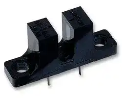
EE-SG3-B
Transmissive Photo Interrupter, Phototransistor, Through Hole, 3.6 mm, 50 mA, 4 V
⚠️ Reference pricing provided. In case of supply shortages, we will connect you with our trusted procurement partners to ensure your project's continuity.
- Manufacturer: OMRON ELECTRONIC COMPONENTS
- Product type: Transmissive Photo Interrupters
- Gap Width: 3.6mm
- Product Range: EE-SG3-B Series
- Sensor Output: Phototransistor
- Forward Voltage: 1.2V
- Sensor Mounting: Through Hole
- Forward Current If: 50mA
- Reverse Voltage Vr: 4V
| Delivery and price | |
|---|---|
| Units per pack | 100 |
| Price | 2.34 € |
| Current stock | 10+ |
| Lead time | 30 days |
Datasheet

## **Photomicrosensor (Transmissive) EE-SG3/EE-SG3-B**

**Be sure to read** _**Precautions**_ **on page 25.**

## ■ **Dimensions**

**Note:** All units are in millimeters unless otherwise indicated.

## ■ **Features**

- Dust-proof model.

- Solder terminal model (EE-SG3).

- PCB terminal model (EE-SG3-B).

**==> picture [254 x 284] intentionally omitted <==**

**----- Start of picture text -----**<br>
Two, 3.2±0.2  13<br>dia. holes pr 25.419±0.1± | 0.2<br>EE-SG3 EE-SG3-B<br>3.6±0.2 A 0.2 6.354 6.354<br>Optical axis . —- co}<br>1.2<br>Four, 0.5<br>Four, 0.25<br>R18 my 7.62±0.3 || 0.8  iz 0.6 ‘tO 2.54±0.3<br>Four, 1.5 Cross section AA<br>2.54<br>Satta Cross section AA fi<br>ce<br>Internal Circuit<br>K C<br>Unless otherwise specified, the<br>tolerances are as shown below.<br>A E Dimensions           Tolerance<br>3 mm max. ±0.3<br>Terminal No.       Name<br>3 < mm ≤ 6 ±0.375<br>A     Anode<br>6 < mm ≤ 10 ±0.45<br>K     Cathode<br>C     Collector 10 < mm ≤ 18 ±0.55<br>E     Emitter 18 < mm ≤ 30 ±0.65<br>**----- End of picture text -----**<br>


## ■ **Absolute Maximum Ratings (Ta = 25** ° **C)**

|**Item**|**Item**|**Symbol**|**Rated value**|
|---|---|---|---|
|**Emitter**|**Forward current**|IF|50 mA<br>(see note 1)|
||**Pulse forward cur-**<br>**rent**|IFP|1 A<br>(see note 2)|
||**Reverse voltage**|VR|4 V|
|**Detector**|**Collector–Emitter**<br>**voltage**|VCEO|30 V|
||**Emitter–Collector**<br>**voltage**|VECO|---|
||**Collector current**|IC|20 mA|
||**Collector dissipa-**<br>**tion**|PC|100 mW<br>(see note 1)|
|**Ambient tem-**<br>**perature**|**Operating**|Topr|–25°C to 85°C|
||**Storage**|Tstg|–30°C to 100°C|
|**Soldering temperature**||Tsol|260°C<br>(see note 3)|


- **Note: 1.** Refer to the temperature rating chart if the ambient temperature exceeds 25°C.

   **2.** The pulse width is 10 μs maximum with a frequency of 100 Hz.

   **3.** Complete soldering within 10 seconds.

■ **Electrical and Optical Characteristics (Ta = 25** ° **C)**

~~Ge~~ **Item Symbol Value Condition Emitter** ~~Ge~~ **Forward voltage** VF 1.2 V typ., 1.5 V max. IF = 30 mA **Reverse current** IR 0.01 μA typ., 10 μA max. VR = 4 V ~~Ge GeO (OO~~ **Peak emission wavelength** λP 940 nm typ. IF = 20 mA **Detector** ~~GG~~ **Light current** IL 2 mA min., 40 mA max. IF = 15 mA, VCE = 10 V ~~GO~~ **Dark current** ID 2 nA typ., 200 nA max. VCE = 10 V, 0 lx ~~GG~~ **Leakage current** ILEAK ----- **Collector–Emitter saturated volt-** VCE (sat) 0.1 V typ., 0.4 V max. IF = 30 mA, IL = 1 mA **age Peak spectral sensitivity wave-** λP 850 nm typ. VCE = 10 V **length** ~~eG~~ **Rising time** tr 4 μs typ. VCC = 5 V, RL = 100 Ω, IL = 5 mA ~~QO~~ **Falling time** tf 4 μs typ. VCC = 5 V, RL = 100 Ω, IL = 5 mA

**EE-SG3/EE-SG3-B** Photomicrosensor (Transmissive)

106

## ■ **Engineering Data**

**Forward Current vs. Collector Dissipation Temperature Rating**

**Forward Current vs. Forward Voltage Characteristics (Typical)**

**Light Current vs. Forward Current Characteristics (Typical)**

**==> picture [164 x 141] intentionally omitted <==**

**----- Start of picture text -----**<br>
60 150<br>IF<br>BERR<br>TENE PC<br>“ .<br>«LAL<br>A<br>SEEANE<br>. \<br>;Pit | .<br>-40 -20 Q 20 4g 60 80 100:<br>Ambient temperature Ta (°C)<br> (mA)  (mW)<br>F C<br>Forward current  I Collector dissipation P<br>**----- End of picture text -----**<br>


**==> picture [304 x 135] intentionally omitted <==**

**----- Start of picture text -----**<br>
Ta = 25°C<br>VCE = 10 V<br>Ta = −30°C<br>CEE Ta = 25°C ED) 28eeepc<br>° Ta = 70°C Pt; TT TT ey<br>N A T: 7<br>. fi ot ttt<br>Le AREA<br>vila] ty<br>°Te) xPane<br>, 0 02 04 06 08 YZ1 12 #14 #16 #18 wt° 10i ti20  ttt30 |40 ty<br>Forward voltage VF (V) Forward current IF (mA)<br> (mA)<br>F<br> (mA)<br>L<br>Forward current  I Light current  I<br>**----- End of picture text -----**<br>


**==> picture [158 x 173] intentionally omitted <==**

**----- Start of picture text -----**<br>
Relative Light Current vs. Ambi-<br>ent Temperature Characteristics<br>(Typical)<br>120<br>IFFCE = 5 V= 20 mA  = 5 VFCE = 5 V= 20 mA  = 5 VCE = 5 V= 20 mA  = 5 V= 20 mA  = 5 V = 5 V = 20 mA  = 5 V = 5 V<br>110 VCE = 5 VIFFCE = 5 V= 20 mA  = 5 VIFFCE = 5 V= 20 mA  = 5 VFCE = 5 V= 20 mA  = 5 VCE = 5 V= 20 mA  = 5 V= 20 mA  = 5 V = 5 V<br>S<br>LO aN<br>90<br>eo<br>”<br>PP |)<br>rrr a Ambient temperature Ta (°C)C)  a i ee er °C)C)C) MT<br> (%)<br>L<br>Relative light current  I<br>**----- End of picture text -----**<br>


**Light Current vs. Collector** − **Emitter Voltage Characteristics (Typical)**

**Dark Current vs. Ambient Temperature Characteristics (Typical)**

**==> picture [476 x 135] intentionally omitted <==**

**----- Start of picture text -----**<br>
Ta = 25°C VCE = 5 VIFFCE = 5 V= 20 mA  = 5 VIFFCE = 5 V= 20 mA  = 5 VFCE = 5 V= 20 mA  = 5 VCE = 5 V= 20 mA  = 5 V= 20 mA  = 5 V = 5 V 0 VCElx = 10 VVCElx = 10 VCElx = 10 Vlx = 10 Vx = 10 V = 10 V se es epee een<br>Pf tt IF = 25 mA |_| 110 1,000 |eeonjeeshenuenn |eeonjeeshenuennse<br>‘ CO Sasleecescee<br>1 IF = 20 mA $0 i peta<br>t te S ee<br>tbe IF = 15 mA a LO aN ee<br>FT |_| IF = 10 mA [| 90 re es aes aes Aa ay.Se eGSe eG eG<br>t ty tt eo =<br>————ce ce _ [ooS=s.===S=s.======<br>IF = 5 mA<br>yt ” a<br>P CO PP |) anaes<br>° 1 2 3 4 5 6 7 8 8 10 rrr a i ee er MT 0.0019 20-40 0 40 20 30 40 60 60 70 80<br>Collector−Emitter voltage VCE (V) Ambient temperature Ta (°C)C) °C)<br>L  (nA)<br> (mA) D<br>L Dark current   I<br>Light current  I Relative light current  I<br>**----- End of picture text -----**<br>


**==> picture [195 x 138] intentionally omitted <==**

**----- Start of picture text -----**<br>
VCE = 5 VIFFCE = 5 V= 20 mA  = 5 VIFFCE = 5 V= 20 mA  = 5 VFCE = 5 V= 20 mA  = 5 VCE = 5 V= 20 mA  = 5 V= 20 mA  = 5 V = 5 V 0 VCElx = 10 VVCElx = 10 VCElx = 10 Vlx = 10 Vx = 10 V = 10 V<br>1,000 |eeonjeeshenuenn |eeonjeeshenuennse es epee een<br>Sasleecescee<br>$0 i peta<br>ee<br>ee<br>re es aes aes Aa ay.Se eGSe eG eG<br>=<br>[ooS=s.===S=s.======<br>a<br>anaes<br>er MT 0.0019 20-40 0 40 20 30 40 60 60 70 80<br>°C)C)C) Ambient temperature Ta (°C)<br> (nA)<br>D<br>Dark current   I<br>**----- End of picture text -----**<br>


**==> picture [494 x 193] intentionally omitted <==**

**----- Start of picture text -----**<br>
Response Time vs. Load Resist- Sensing Position Characteristics  Sensing Position Characteristics<br>ance Characteristics (Typical) (Typical) (Typical)<br>120<br>1000 ee Soa 120<br>aa  SO es| Ta = 25VCC = 5 V  | °C an too VTa = 25IFCE= 20 mA  = 10 V °C   100 = Ta = 25IVFCE= 20 mA  = 10 V °C<br>(Center of<br>a optical axis) Hod 80<br>a a Oa a 80 =<br>d<br>oe Seta Ph 60 P| | \\ | i<br>oe w ale<br>A ee ce : 40 \ | 1 |<br>Sell eo «o fill<br>POSSS a en| 20 20 P|)| iN\|<br>0<br>CLEaatiME ;Pf | LT −2.0 PF} −1.5 − it 1.0 −0.5 | 0 0.5 aSLL 1.0 1.5 2.0<br>0.01 01 1 10 -2 -f 0 1 2 3 4<br>Load resistance RL (kΩ) Distance d (mm)<br>Distance d (mm)<br>Response Time Measurement<br>Circuit<br>s)μ  (%)L  (%)L (Center of optical axis)<br>Response time tr, tf ( Relative light current  I Relative light current  I<br>**----- End of picture text -----**<br>


**==> picture [131 x 89] intentionally omitted <==**

**----- Start of picture text -----**<br>
Input<br>—t<br>90 %<br>Output 10 %<br>° f } ——t<br>tr tf<br>Input i vec<br>y=K |<br>Output<br>**----- End of picture text -----**<br>


**EE-SG3/EE-SG3-B** Photomicrosensor (Transmissive)

107
Updated at February 9, 2023
About Novapart
Novapart is a B2B electronic component broker specialising in stock shortages and cost reduction. We source hard-to-find parts and identify compliant alternatives across a catalogue of 410,000+ components from 500+ manufacturers.
Learn more →Stock Shortage Specialist
When a component is unavailable, discontinued or has an unacceptable lead time, we tap into our network of vetted European and Asian distributors to source what you need — without compromising on quality or traceability.
Request a quote →Compliant Alternatives
We identify pin-to-pin, electrically equivalent substitutes that meet the same certifications (RoHS, AEC-Q100, REACH) as your original specification — validated against datasheets, not just part numbers. Often at a lower cost.
BOM Analysis service →