


ECMF04-4HSWM10Y
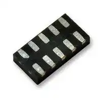
Common Mode Filter, 0.1A, AEC-Q101, 2.6mm x 1.35mm x 0.5mm
- Manufacturer: STMICROELECTRONICS
- Product type: SMD Common Mode Chokes / Filters
- SVHC: No SVHC (25-Jun-2025)
- Impedance: -
- Inductance: -
- Product Range: ECMF Series
- Product Width: 1.35mm
- Qualification: -
- Product Height: 0.5mm
- Product Length: 2.56mm
- DC Current Rating: 100mA
- DC Resistance Max: 5.5ohm
- Common Mode Filter Case: 2.6mm x 1.35mm x 0.5mm
- Inductor Case / Package: -
- Operating Temperature Max: 125°C
- Operating Temperature Min: -55°C
| Delivery and price | |
|---|---|
| Units per pack | 3000 |
| Price | 0.232 € |
| Current stock | 10+ |
| Lead time | 30 days |
**ECMF04-4HSWM10**

Datasheet

## Common mode filter with ESD protection for high speed serial interface

## **Features**

**==> picture [125 x 92] intentionally omitted <==**

- Very large differential bandwidth to comply with HDMI Full HD, MIPI, USB2.0, USB3.2 Gen 1, Display Port and other high speed serial interfaces

- High common mode attenuation on WLAN frequencies:

   - 28 dB at 2.4 GHz and -16 dB at 5.0 GHz

- Very good attenuation at LTE, GSM and GPS frequencies

- Large bandwidth: 4.2 GHz

- Low PCB space consumption

- Thin package for compact applications: 0.55 mm max.

QFN-10L 2.6 x 1.35 x 0.5

- High reduction of parasitic elements through integration

- RoHS package

## **Exceed the following standards**

**==> picture [159 x 201] intentionally omitted <==**

**----- Start of picture text -----**<br>
D1+ Con 1 10 D1+ IC<br>D1- Con 2 9 D1- IC<br>GND 3 8 GND<br>D2+ Con 4 7 D2+ IC<br>D2- Con 5 6 D2- IC<br>Product status link<br>ECMF04-4HSWM10<br>Product summary<br>Order code ECMF04-4HSWM10<br>**----- End of picture text -----**<br>


- IEC 61000-4-2, level 4:

   - ±15 kV (air discharge)

   - ±8 kV (contact discharge)

## **Applications**

- Mobile phones

- Notebook, laptop

- Portable devices

- PND

## **Description**

The ECMF04-4HSWM10 is a highly integrated common mode filter designed to suppress EMI/RFI common mode noise on high speed differential serial buses like HDMI Full HD, MIPI, Display Port and other high speed serial interfaces.

The device has a very large differential bandwidth to comply with these standards and can protect and filter two differential lanes.

**DS10228** - **Rev 3** - **March 2021** For further information contact your local STMicroelectronics sales office.

www.st.com

**ECMF04-4HSWM10 Characteristics**

## **1 Characteristics**

**Table 1. Absolute maximum ratings (Tamb = 25 °C)**

|**Symbol**|**Parameter**|**Parameter**|**Value**|**Unit**|
|---|---|---|---|---|
|VPP|Peak pulse voltage|IEC 61000-4-2:<br>Contact discharge<br>Air discharge|8<br>16|kV|
|IRMS|Maximum RMS current||100|mA|
|Top|Operating ambient temperature range||-55 to +125|°C|
|Tj|Maximum junction temperature||125||
|Tstg|Storage temperature range||-55 to +150||


**Figure 1. Electrical characteristics (definitions)**

|VRM<br>Maximum stand-off voltage<br>VCL<br>Clamping voltage at peak pulse current IPP<br>IRM<br>Leakage current at VRM<br>IPP<br>Peak pulse current<br>VBR<br>Breakdown voltage<br>RDC<br>DC serial resistance<br>fC<br>Differential cut off frequency|**IRM**<br>**IR**<br>**IPP**<br>**I**|**IRM**<br>**IR**<br>**IPP**<br>**I**|**VCL**<br>**VBR**<br>**VRM**<br>**V**|
|---|---|---|---|
|||**IRM**<br>**IR**<br>**IPP**||
|||||
|||||
|||||
||||**VBR**<br>**VRM**|


**Table 2. Electrical characteristics (Tamb = 25 °C)**

|**Symbol**|**Test conditions**|**Min.**|**Typ.**|**Max.**|**Unit**|
|---|---|---|---|---|---|
|VBR|IR= 1 mA|4.5|5.5||V|
|IRM|VRM= 3 V per line|||100|nA|
|RDC|DC serial resistance||5||Ω|
|fC|-3 dB differential mode cut-off frequency||4.2||GHz|


**Table 3. Pin description**

|**Pin number**|**Description**|**Pin number**|**Description**|
|---|---|---|---|
|1|D1+ to connector|6|D2- to IC|
|2|D1- to connector|7|D2+ to IC|
|3|GND|8|GND|
|4|D2+ to connector|9|D1- to IC|
|5|D2- to connector|10|D1+ to IC|


**DS10228** - **Rev 3**

**page 2/14**

**ECMF04-4HSWM10 Characteristics (curves)**

## **1.1 Characteristics (curves)**

**==> picture [487 x 171] intentionally omitted <==**

**----- Start of picture text -----**<br>
Figure 2. Differential attenuation versus frequency    Figure 3. Common mode attenuation versus frequency<br>(Z0_DIFF = 100 Ω) (Z0_COM = 50 Ω)<br>SDD21(dB) SCC21(dB)<br>0 ||. -5eeTT NN<br>-2 \‘ Co40 CNN \ Oy,<br>NI 7 \<br>° -25. f<br>~ -30 a A<br>f(Hz) f(Hz)<br>5 ve-45 IT<br>**----- End of picture text -----**<br>


**Figure 4. ESD response to IEC61000-4-2 (+8 kV contact Figure 5. ESD response to IEC61000-4-2 (-8 kV contact discharge) discharge)**

**Figure 6. HDMI2.0 - 5.94 Gbps eye diagram without device (with worst cable and equalizer)**

**Figure 7. HDMI2.0 - 5.94 Gbps eye diagram with device (with worst cable and equalizer)**

**DS10228** - **Rev 3**

**page 3/14**

**ECMF04-4HSWM10 Characteristics (curves)**

**Figure 8. HDMI1.4 3.35 Gbps eye diagram without ECMF04-4HSWM10**

**Figure 10. USB3.2 Gen 1 5.0 Gbps eye diagram without ECMF04-4HSWM10 (with worst cable and equalizer)**

**Figure 12. MIPI D-PHY 2.5 Gbps long reference channel eye diagram without ECMF04-4HSWM10**

**Figure 9. HDMI1.4 3.35 Gbps eye diagram with ECMF04-4HSWM10**

**Figure 11. USB3.2 Gen 1 5.0 Gbps eye diagram with ECMF04-4HSWM10 (with worst cable and equalizer)**

**Figure 13. MIPI D-PHY 2.5 Gbps long reference channel eye diagram with ECMF04-4HSWM10**

**DS10228** - **Rev 3**

**page 4/14**

**ECMF04-4HSWM10 Characteristics (curves)**

**==> picture [398 x 163] intentionally omitted <==**

**----- Start of picture text -----**<br>
Figure 15. Differential an common mode impedance<br>Figure 14. TDR<br>versus frequency<br>Z(Ω)<br>compensation ee<br>ep 1eg sfee Ati<br>——— |<br>i After compensation ee ee ee=a ———es ee==>2<br>jf t | 1e2 JN ZCOM<br>LS ieee Dee eee ee Ree ene eee —| ee eei el ONYa, SE |<br>161—.a—— ZDIFF YY<br>|<br>RF R© R& RF& R© R& R& RR& A& wT TTT f(Hz)<br>**----- End of picture text -----**<br>


**DS10228** - **Rev 3**

**page 5/14**

**ECMF04-4HSWM10 Application information**

## **2**

## **Application information**

**Figure 16. HDMI schematic**

**==> picture [216 x 309] intentionally omitted <==**

**----- Start of picture text -----**<br>
ECMF04<br>D0<br>eeee 2<br>D1<br>seee eee<br>ECMF04<br>D2<br>ee [2-0-0] —<br>Clock<br>a ——<br>SDA HDP_IC<br>SCL SDA_IC<br>GND GND SCL_IC<br>CEC CEC_IC<br>VDD_CEC FAULT<br>HDMI2C1-6C1<br>troce CSI<br>nno AMI<br>c I D<br>M H<br>D<br>H<br>PHD LITUYTI CEAH+ CEHA-<br>OUTV5 _ VDDV5 _ CCCDIF __ CIDDV _<br>DV<br>**----- End of picture text -----**<br>


More application information available in following AN:

- AN4356: "Antenna desense on handheld equipment"

- AN4511: "Common mode filters"

- AN4540: "MHL link filtering and protection"

**DS10228** - **Rev 3**

**page 6/14**

**ECMF04-4HSWM10 Package information**

## **3 Package information**

In order to meet environmental requirements, ST offers these devices in different grades of ECOPACK packages, depending on their level of environmental compliance. ECOPACK specifications, grade definitions and product status are available at: www.st.com. ECOPACK is an ST trademark.

## **3.1 QFN-10L package information**

## **Figure 17. QFN10L package outline**

**==> picture [8 x 8] intentionally omitted <==**

**----- Start of picture text -----**<br>
D<br>**----- End of picture text -----**<br>


**==> picture [198 x 104] intentionally omitted <==**

**==> picture [8 x 7] intentionally omitted <==**

**----- Start of picture text -----**<br>
E<br>**----- End of picture text -----**<br>


## TOP VIEW

**==> picture [266 x 247] intentionally omitted <==**

**----- Start of picture text -----**<br>
SIDE VIEW<br>e<br> b<br>A<br>A1<br> L<br>**----- End of picture text -----**<br>


**DS10228** - **Rev 3**

**page 7/14**

**ECMF04-4HSWM10 QFN10L package information**

**Table 4. QFN10L package mechanical data**

||**Dimensions**|**Dimensions**|**Dimensions**|
|---|---|---|---|
|**Ref.**|**Millimeters**|||
||**Min.**|**Typ.**|**Max.**|
|A|0.45|0.50|0.55|
|A1|0.00|0.02|0.05|
|b|0.15|0.20|0.25|
|D|2.55|2.60|2.65|
|E|1.30|1.35|1.40|
|e||0.50||
|L|0.40|0.50|0.60|


**Figure 18. Footprint recommendations (mm)**

**==> picture [46 x 51] intentionally omitted <==**

**DS10228** - **Rev 3**

**page 8/14**

**ECMF04-4HSWM10 PCB assembly recommendations**

## **4 PCB assembly recommendation**

## **Figure 19. Recommended PCB layout**

**==> picture [381 x 8] intentionally omitted <==**

**----- Start of picture text -----**<br>
Connector Host<br>**----- End of picture text -----**<br>


**Figure 20. PCB stack dimensions**

**==> picture [202 x 119] intentionally omitted <==**

**----- Start of picture text -----**<br>
40 µm<br>105 µm<br>εr [= 4.28]<br>i<br>**----- End of picture text -----**<br>


## **4.1**

## **Solder paste**

1. Halide-free flux qualification ROL0 according to ANSI/J-STD-004.

2. “No clean” solder paste is recommended.

3. Offers a high tack force to resist component movement during high speed.

4. Use solder paste with fine particles: powder particle size is 20-38 μm.

**DS10228** - **Rev 3**

**page 9/14**

**ECMF04-4HSWM10 QFN-10L packing information**

**==> picture [474 x 238] intentionally omitted <==**

**----- Start of picture text -----**<br>
ky<br>4.2 QFN-10L packing information<br>Figure 22. Package orientation in reel<br>Figure 21. Marking<br>XX<br>a<br>Pin 1 located according to EIA-481<br>Note: Pocket dimensions are not on scale<br>\<br>Dot indicates pin 1 Pocket shape may vary depending on package<br>XX: Marking<br>**----- End of picture text -----**<br>


**Figure 23. Tape and reel orientation**

**Figure 24. Reel dimensions (mm)**

**==> picture [155 x 95] intentionally omitted <==**

**----- Start of picture text -----**<br>
Ø 180 max 14.4<br>2±0.5<br>Ø 13<br>Ø 60  Ø 20.2 min<br>**----- End of picture text -----**<br>


**Figure 25. Inner box dimensions (mm)**

**==> picture [106 x 132] intentionally omitted <==**

**----- Start of picture text -----**<br>
30<br>205<br>205<br>**----- End of picture text -----**<br>


**DS10228** - **Rev 3**

**page 10/14**

**ECMF04-4HSWM10 Solder reflow**

**Figure 26. Tape and reel outline**

## **4.3 Solder reflow**

**Figure 27. ST ECOPACK[®] recommended soldering reflow profile for PCB mounting**

**==> picture [244 x 132] intentionally omitted <==**

**----- Start of picture text -----**<br>
240-245 °C<br>Temperature (°C)<br>250 -2 °C/s<br>2 - 3 °C/s<br>200 60 sec<br>poppet [| (90m ax) -3 °C/s o y<br>150 pt  fee |<br>-6° C/s<br>100<br>EZ [ane,] et Ee NG<br>0.9 °C/s<br>50<br>e o<br>Time (s)<br>0 Pit 30 60 90 | 120 || | 150 TT| 180 210 TN 240 270 300<br>**----- End of picture text -----**<br>


_Note:_

_Minimize air convection currents in the reflow oven to avoid component movement. Maximum soldering profile corresponds to the latest IPC/JEDEC J-STD-020._

**DS10228** - **Rev 3**

**page 11/14**

**ECMF04-4HSWM10 Ordering information**

## **5 Ordering information**

**Figure 28. Ordering information scheme**

|ECMF 04 – 4 HS W M10|ECMF 04 – 4 HS W M10|ECMF 04 – 4 HS W M10|ECMF 04 – 4 HS W M10|ECMF 04 – 4 HS W M10|ECMF 04 – 4 HS W M10|ECMF 04 – 4 HS W M10|
|---|---|---|---|---|---|---|
|Function|||||||
|Common mode filter with ESD protection|||||||
|Number if lines|||||||
|04 = 4 filtered lines|||||||
|Number of ESD protected lines|||||||
|4 lines with ESD protection|||||||
|Version|||||||
|HS = High Speed|||||||
|Application|||||||
|WLAN 2.4 GHz|||||||
|Package|||||||
|M10: µQFN-10L|||||||


|**Order code**|**Marking**|**Package**|**Weight**|**Base qty.**|**Delivery mode**|
|---|---|---|---|---|---|
|ECMF04-4HSWM10|KW(1)|µQFN-10L|5 mg|3000|Tape and reel|


_1. The marking can be rotated by 90° to differentiate assembly location_

**DS10228** - **Rev 3**

**page 12/14**

**ECMF04-4HSWM10**

## **Revision history**

**Table 5. Document revision history**

|**Date**|**Version**|**Changes**|
|---|---|---|
|10-Jun-2014|1|Initial release.|
|08-Jan-2018|2|Updated Table 1.|
|16-Mar-2021|3|UpdatedFigure 8andFigure 9.<br>AddedFigure 10,Figure 11andFigure 15.|


**DS10228** - **Rev 3**

**page 13/14**

**ECMF04-4HSWM10**

## **IMPORTANT NOTICE – PLEASE READ CAREFULLY**

STMicroelectronics NV and its subsidiaries (“ST”) reserve the right to make changes, corrections, enhancements, modifications, and improvements to ST products and/or to this document at any time without notice. Purchasers should obtain the latest relevant information on ST products before placing orders. ST products are sold pursuant to ST’s terms and conditions of sale in place at the time of order acknowledgement.

Purchasers are solely responsible for the choice, selection, and use of ST products and ST assumes no liability for application assistance or the design of Purchasers’ products.

No license, express or implied, to any intellectual property right is granted by ST herein.

Resale of ST products with provisions different from the information set forth herein shall void any warranty granted by ST for such product.

ST and the ST logo are trademarks of ST. For additional information about ST trademarks, please refer to www.st.com/trademarks. All other product or service names are the property of their respective owners.

Information in this document supersedes and replaces information previously supplied in any prior versions of this document.

© 2021 STMicroelectronics – All rights reserved

**DS10228** - **Rev 3**

**page 14/14**
Updated at June 5, 2026
STMicroelectronics is a global leader in the semiconductor industry, recognized for developing highly integrated, energy-efficient solutions that power modern electronics. With a strong focus on innovation, ST provides a comprehensive portfolio of microelectronics that address the demanding requirements of industrial, automotive, communications, and consumer applications. Our extensive selection of STMicroelectronics components is built around a robust lineup of discrete semiconductors and circuit protection devices. We offer a wide variety of single MOSFETs, Schottky diodes, and fast and ultrafast recovery rectifier diodes, designed to deliver exceptional efficiency and thermal performance in power management and conversion systems. For robust circuit protection, our inventory features hundreds of transient voltage suppressors and TVS diodes that safeguard sensitive electronic components against destructive voltage spikes. In addition to core power discretes like TRIACs, SCRs, bipolar transistors, and single IGBTs, our STMicroelectronics range includes specialized integrated passive filters and MEMS sensors. Furthermore, ST offers advanced integrated passive devices, such as baluns and RF filters, which utilize high-quality monolithic RF IPD processes on glass or high-resistance silicon substrates. These components provide competitive cost structures, reduced power losses, and simplified RFIC-to-antenna matching, ensuring optimal system performance and delivering the reliability required for next-generation wireless and power designs.
About Novapart
Novapart is a B2B electronic component broker specialising in stock shortages and cost reduction. We source hard-to-find parts and identify compliant alternatives across a catalogue of 410,000+ components from 500+ manufacturers.
Learn more →Stock Shortage Specialist
When a component is unavailable, discontinued or has an unacceptable lead time, we tap into our network of vetted European and Asian distributors to source what you need — without compromising on quality or traceability.
Request a quote →Compliant Alternatives
We identify pin-to-pin, electrically equivalent substitutes that meet the same certifications (RoHS, AEC-Q100, REACH) as your original specification — validated against datasheets, not just part numbers. Often at a lower cost.
BOM Analysis service →