
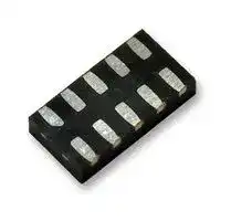


ECMF04-4HSWM10
Filter, Common Mode, 2.6mm x 1.35mm x 0.5mm
- Manufacturer: STMICROELECTRONICS
- Product type:
- SVHC: No SVHC (25-Jun-2025)
- No. of Pins: 10Pins
- Product Range: ECMF Series
- Filter Circuit: Common-Mode
- EMI Filter Type: Common Mode Filter with ESD Protection
- No. of Data Lines: 4 Data Lines
- Filter Case / Package: µQFN
| Delivery and price | |
|---|---|
| Units per pack | 9000 |
| Price | 0.288 € |
| Current stock | 10+ |
| Lead time | 30 days |
## **ECMF04-4HSWM10**

## Common-mode filter with ESD protection for high-speed serial interfaces

**Datasheet** - **production data**

## **Features**

- Very large differential bandwidth to comply with HDMI 2.0, USB3.0, MIPI, DisplayPort and other high speed serial interfaces

- High common mode attenuation on WLAN frequencies:

   - 28 dB at 2.4 GHz and -16 dB at 5.0 GHz

- Very good attenuation at LTE, GSM and GPS frequencies

**==> picture [110 x 10] intentionally omitted <==**

**----- Start of picture text -----**<br>
µQFN-10L 2.60 x 1.35 mm<br>**----- End of picture text -----**<br>


- Large bandwidth: 4.2GHz

- Very low PCB space consumption

- Thin package: 0.55 mm max.

- Lead-free package

## **Figure 1. Pin configuration (top view)**

**==> picture [143 x 158] intentionally omitted <==**

**----- Start of picture text -----**<br>
D1+ 1 10 D1+<br>D1- 2 9 D1-<br>GND 3 8 GND<br>D2+ 4 7 D2+<br>D2- 5 6 D2-<br>**----- End of picture text -----**<br>


- High reduction of parasitic elements through integration

## **Complies with the following standards:**

- IEC 61000-4-2 level 4:

   - ±15 kV (air discharge)

   - ±8 kV (contact discharge)

## **Applications**

- Set top box

- Streaming box

- Game console

- Notebook, laptop

- Portable devices

## **Description**

The ECMF04-4HSWM10 is a highly integrated common-mode filter designed to suppress EMI/RFI common mode noise on high-speed differential serial buses like HDMI 2.0, USB3.0, Ethernet, MIPI, DisplayPort and other high-speed serial interfaces. The device has a very large differential bandwidth to comply with these standards and can also protect and filter 2 differential lanes.

June 2014

DocID026032 Rev 1

1/13

This is information on a product in full production.

_www.st.com_

**Contents**

**ECMF04-4HSWM10**

|**Contents**|**Contents**|
|---|---|
|**1**|**Characteristics  . . . . . . . . . . . . . . . . . . . . . . . . . . . . . . . . . . . . . . . . . . . . . 3**|
|**2**|**Application information  . . . . . . . . . . . . . . . . . . . . . . . . . . . . . . . . . . . . . . 8**|
|**3**|**PCB layout recommendations . . . . . . . . . . . . . . . . . . . . . . . . . . . . . . . . . 9**|
|**4**|**Package information . . . . . . . . . . . . . . . . . . . . . . . . . . . . . . . . . . . . . . . . 10**|
|**5**|**Ordering information  . . . . . . . . . . . . . . . . . . . . . . . . . . . . . . . . . . . . . . . 12**|
|**6**|**Revision history  . . . . . . . . . . . . . . . . . . . . . . . . . . . . . . . . . . . . . . . . . . . 12**|


2/13

DocID026032 Rev 1

**ECMF04-4HSWM10**

**Characteristics**

## **1 Characteristics**

**Table 1. Absolute maximum ratings (Tamb = 25 °C)**

||**Table 1. Absolute maximum ratings (Tamb = 25 °C)**|**Table 1. Absolute maximum ratings (Tamb = 25 °C)**|||
|---|---|---|---|---|
|**Symbol**|**Parameter**||**Value**|**Unit**|
|VPP|Peak pulse voltage|IEC 61000-4-2<br>Contact discharge (connector side)<br>Air discharge (connector side)|8<br>15|kV|
|IRMS|Maximum RMS current||100|mA|
|Top|Operating temperature range||-40 to +85|°C|
|Tj|Maximum junction temperature||125|°C|
|Tstg|Storage temperature range||- 55 to +150|°C|


**Figure 2. Electrical characteristics (definitions)**

**==> picture [324 x 158] intentionally omitted <==**

**----- Start of picture text -----**<br>
I<br>Symbol Parameter<br>VBR = Breakdown voltage<br>IRM = Leakage current @ VRM<br>VRM = Stand-off voltage<br>IR = Breakdown current VBR VRM V<br>IRM<br>IR<br>**----- End of picture text -----**<br>


**Table 2. Electrical characteristics (Tamb = 25 °C)**

|**Symbol**|**Test conditions**|**Min.**|**Typ.**|**Max.**|**Unit**|
|---|---|---|---|---|---|
|VBR|IR= 1 mA|4.5|5.5||V|
|IRM|VRM= 3 V per line|||100|nA|
|RDC|DC serial resistance||5||Ω|
|FC|-3dB differential mode cut-off frequency||4.2||GHz|


DocID026032 Rev 1

3/13

**Characteristics**

**ECMF04-4HSWM10**

**Table 3. Pin description**

|**Pin number**|**Description**|**Pin number**|**Description**|
|---|---|---|---|
|1|D1+ to connector|6|D2- to IC|
|2|D1- to connector|7|D2+ to IC|
|3|GND|8|GND|
|4|D2+ to connector|9|D1- to IC|
|5|D2- to connector|10|D1+ to IC|


## **Figure 3. Differential attenuation versus frequency (Z0 diff = 100** Ω **)**

**==> picture [333 x 291] intentionally omitted <==**

**----- Start of picture text -----**<br>
SDD21 (dB)<br>0<br>Serr<br>-1<br>CLIT ee |<br>-2<br>OI LUIS<br>-3<br>CE LAINEAM E<br>-4 STN TIN<br>-5<br>10M 30M 100M 300M 1G 3G<br>F/Hz<br>Lane #1 Lane #2<br>**----- End of picture text -----**<br>


4/13 DocID026032 Rev 1 ~~>~~

**ECMF04-4HSWM10**

**Characteristics**

**==> picture [350 x 303] intentionally omitted <==**

**----- Start of picture text -----**<br>
Figure 4. Common mode attenuation versus frequency (Z0 com = 50  Ω )<br>SCC21 (dB)<br>0<br>-5<br>-10<br>SN<br>-15 Iw<br>k<br>-20<br>-25<br>-30<br>-35<br>-40<br>10M 30M 100M 300M 1G 3G<br>Lane #1 F/Hz Lane #2<br>**----- End of picture text -----**<br>


## **Figure 5. ESD response to IEC61000-4-2 (+8 kV contact discharge)**

**==> picture [338 x 119] intentionally omitted <==**

**----- Start of picture text -----**<br>
20 V/di v<br>LOUTPUT l | l t max<br>I|<br>|| e 1 VPP: ESD peak voltage<br>a \ e@ 2 VCL :clamping voltage @ 30 ns<br>| | e@ 3 VCL :clamping voltage @ 60 ns<br>\|@ 4 VCL :clamping voltage @ 100 ns<br>|| j<br>| i I i<br>@ 1 72.1 V an i<br>| | { \<br>++|+{<br>I 2 13.1 V | 3 11.2 V \ 4 7.1 V<br>**----- End of picture text -----**<br>


DocID026032 Rev 1

5/13

**Characteristics**

**ECMF04-4HSWM10**

**==> picture [320 x 212] intentionally omitted <==**

**----- Start of picture text -----**<br>
Figure 6. ESD response to IEC61000-4-2 (-8 kV contact discharge)<br>20 V/di v<br>TII<br>'‘ 1<br>| | |<br>5 ' ‘ ‘<br>= :' ‘ Pheecdinrlda<br>L-----4--- 5-5 perenne ni, ere<br>' ‘ 1<br>|meccitho eabeaeeee eS ce say vJtg Ss let OE RdSend cl c:c:c:cicisicicisis::<br>' 1<br>! |<br>'11<br>ii I<br>OUTPUT ' i | 4 -3.0 V<br>' 2 -10.3 V H‘<br>:‘ 3 -9.2 V ‘<br>|||<br>1 -65.4 V '‘ ‘<br>|||<br>4' i<br>||'<br>'1 @ 1 VPP: ESD peak voltage<br>nL1 2 VCL :clamping voltage @ 30 ns<br>'; ‘ @ 3 VCL :clamping voltage @ 60 ns<br>1 ! e 4 VCL :clamping voltage @ 100 ns<br>: ‘<br>ee EE SSnS: 1SS a ‘(nS SD<br>z 1 | | 20 ns/di v<br>**----- End of picture text -----**<br>


**Figure 7. HDMI2.0 5.94 Gbps eye diagram without ECMF04-4HSWM10 (evaluation board with SMA connector)**

**Figure 8. HDMI2.0 5.94 Gbps eye diagram with ECMF04-4HSWM10 (evaluation board with SMA connector)**

6/13

DocID026032 Rev 1

**ECMF04-4HSWM10**

**Characteristics**

**Figure 9. HDMI1.4 3.35 Gbps eye diagram Figure 10. HDMI1.4 3.35 Gbps eye diagram with without ECMF04-4HSWM10 ECMF04-4HSWM10**

**==> picture [258 x 122] intentionally omitted <==**

**----- Start of picture text -----**<br>
250mV/div 250mV/div<br>xenX.<br>49.8ps/div<br>49.8ps/div<br>**----- End of picture text -----**<br>


**Figure 11. TDR**

DocID026032 Rev 1

7/13

**ECMF04-4HSWM10**

**Application information**

## **2 Application information**

**==> picture [128 x 11] intentionally omitted <==**

**----- Start of picture text -----**<br>
Figure 12. HDMI schematic<br>**----- End of picture text -----**<br>


**==> picture [366 x 529] intentionally omitted <==**

**----- Start of picture text -----**<br>
ECMF04<br>a D0 <>0)<br>D1<br>ECMF04<br>D2<br>eea ><br>Clock<br>SDA HDP_IC<br>SCL SDA_IC<br>GND GND SCL_IC<br>CEC CEC_IC<br>VDD_CEC FAULT<br>HDMI2C1-6C1<br>Figure 13. USB3.0 application<br>Connector ECMF02-4CMX8<br>| Lo ||<br>Vbus | Programmable en |) surerspeeo<br>USB2.0 OCP<br>D+ ——__-<br>Q0000 |<br>Q0000 |<br>| D-<br>|<br>ID | ars |<br>— i<br>USB 3.0<br>GND<br>transceiver<br>ECMF04-4HSWM10<br>USB3.0<br>Txp<br>| 14] ST<br>| Txn 12] E)||<br>|<br>i Rxp i<br>Rxn<br>HDMI ASIC<br>HDMI connector<br>HPD UTILITY HEAC+ HEAC-<br>5V_OUT VDD_5V VDD_CFC_IC VDD_IC<br>**----- End of picture text -----**<br>


8/13

DocID026032 Rev 1

**ECMF04-4HSWM10**

**PCB layout recommendations**

## **3 PCB layout recommendations**

**==> picture [193 x 11] intentionally omitted <==**

**----- Start of picture text -----**<br>
Figure 14. PCB layout recommendations<br>**----- End of picture text -----**<br>


**==> picture [381 x 257] intentionally omitted <==**

**----- Start of picture text -----**<br>
Connector Host<br>Pad layout 5000 µm<br>350 µm<br>150 µm<br>350 µm<br>Differential Differential<br>lanes lanes<br>(Z0 = 100 ) (Z0 = 100 )<br>330 µm<br>Figure 15. PCB stack dimensions<br>40 µm<br>105 µm<br>ε r  [= 4.28]<br>170 µm<br>170 µm<br>**----- End of picture text -----**<br>


DocID026032 Rev 1 9/13 ~~Sr~~

**ECMF04-4HSWM10**

**Package information**

## **4 Package information**

- Epoxy meets UL94, V0

- Lead-free package

In order to meet environmental requirements, ST offers these devices in different grades of ECOPACK[®] packages, depending on their level of environmental compliance. ECOPACK[®] specifications, grade definitions and product status are available at: _www.st.com._ ECOPACK[®] is an ST trademark.

## **Figure 16. µQFN-10L dimension definitions**

**==> picture [216 x 287] intentionally omitted <==**

**----- Start of picture text -----**<br>
Top view<br>D<br>Idex area<br>E<br>Side view<br>A1<br>A<br>Bottom view<br>e b<br>1 5<br>PIN # 1 ID<br>L<br>10 6<br>**----- End of picture text -----**<br>


**Table 4. µQFN-10L dimension values**

||**Table 4.µQFN-10L dimension values**|**Table 4.µQFN-10L dimension values**|**Table 4.µQFN-10L dimension values**|**Table 4.µQFN-10L dimension values**|**Table 4.µQFN-10L dimension values**|**Table 4.µQFN-10L dimension values**|
|---|---|---|---|---|---|---|
|**Ref.**|**Dimensions**||||||
||**Millimeters**|||**Inches**|||
||**Min.**|**Typ.**|**Max.**|**Min.**|**Typ.**|**Max.**|
|A|0.45|0.50|0.55|0.018|0.020|0.022|
|A1|0.00|0.02|0.05|0.00|0.0008|0.002|
|b|0.15|0.20|0.25|0.006|0.008|0.010|
|D|2.55|2.60|2.65|0.1|0.102|0.104|
|E|1.30|1.35|1.40|0.051|0.053|0.055|
|e||0.50|||0.020||
|L|0.40|0.50|0.60|0.016|0.020|0.024|


DocID026032 Rev 1

10/13

**ECMF04-4HSWM10**

**Package information**

**==> picture [405 x 148] intentionally omitted <==**

**----- Start of picture text -----**<br>
Figure 17. Footprint Figure 18. Marking<br>0.20<br>0.70<br>1.75<br>KW<br>0.50<br>**----- End of picture text -----**<br>


_Note: Product marking may be rotated by multiples of 90° for assembly plant differentiation. In no case should this product marking be used to orient the component for its placement on a PCB. Only pin 1 mark is to be used for this purpose._

**Figure 19. Tape and reel specifications**

**==> picture [389 x 217] intentionally omitted <==**

**----- Start of picture text -----**<br>
Dot identifying Pin A1 location Ø 1.55±0.05<br>2.0±0.05 4.0±0.1<br>0.20±0.05<br>1.55±0.05 4.0<br>0.65±0.05<br>All dimensions are typical values in mm User direction of unreeling<br>1.75±0.1<br>2.8±0.05<br>3.5±0.05<br>8.0 +0.3 / -0.1<br>**----- End of picture text -----**<br>


DocID026032 Rev 1

11/13

**Ordering information**

**ECMF04-4HSWM10**

## **5 Ordering information**

**==> picture [191 x 11] intentionally omitted <==**

**----- Start of picture text -----**<br>
Figure 20. Ordering information scheme<br>**----- End of picture text -----**<br>


**==> picture [393 x 239] intentionally omitted <==**

**----- Start of picture text -----**<br>
ECMF 04 – 4 HS W M10<br>Function<br> Common mode filter with ESD protection<br>Number if lines<br> 04 = 4 filtered lines<br>Number of ESD protected lines<br> 4 lines with ESD protection<br>Version<br> HS = High Speed<br>Application<br>WLAN 2.4 GHz<br>Package<br> M10: µQFN-10L<br>**----- End of picture text -----**<br>


**Table 5. Ordering information**

|**Order code**|**Marking(1)**|**Package**|**Weight**|**Base qty**|**Delivery mode**|
|---|---|---|---|---|---|
|ECMF04-4HSWM10|KW|µQFN-10L|5.00 mg|3000|Tape and reel|


1. The marking can be rotated by multiples of 90° to differentiate assembly location

## **6 Revision history**

**Table 6. Document revision history**

|**Date**|**Revision**||**Changes**|
|---|---|---|---|
|10-Jun-2014|1|Initial release.||


12/13

DocID026032 Rev 1

**ECMF04-4HSWM10**

## **Please Read Carefully:**

Information in this document is provided solely in connection with ST products. STMicroelectronics NV and its subsidiaries (“ST”) reserve the right to make changes, corrections, modifications or improvements, to this document, and the products and services described herein at any time, without notice.

All ST products are sold pursuant to ST’s terms and conditions of sale.

Purchasers are solely responsible for the choice, selection and use of the ST products and services described herein, and ST assumes no liability whatsoever relating to the choice, selection or use of the ST products and services described herein.

No license, express or implied, by estoppel or otherwise, to any intellectual property rights is granted under this document. If any part of this document refers to any third party products or services it shall not be deemed a license grant by ST for the use of such third party products or services, or any intellectual property contained therein or considered as a warranty covering the use in any manner whatsoever of such third party products or services or any intellectual property contained therein.

**UNLESS OTHERWISE SET FORTH IN ST’S TERMS AND CONDITIONS OF SALE ST DISCLAIMS ANY EXPRESS OR IMPLIED WARRANTY WITH RESPECT TO THE USE AND/OR SALE OF ST PRODUCTS INCLUDING WITHOUT LIMITATION IMPLIED WARRANTIES OF MERCHANTABILITY, FITNESS FOR A PARTICULAR PURPOSE (AND THEIR EQUIVALENTS UNDER THE LAWS OF ANY JURISDICTION), OR INFRINGEMENT OF ANY PATENT, COPYRIGHT OR OTHER INTELLECTUAL PROPERTY RIGHT.**

**ST PRODUCTS ARE NOT DESIGNED OR AUTHORIZED FOR USE IN: (A) SAFETY CRITICAL APPLICATIONS SUCH AS LIFE SUPPORTING, ACTIVE IMPLANTED DEVICES OR SYSTEMS WITH PRODUCT FUNCTIONAL SAFETY REQUIREMENTS; (B) AERONAUTIC APPLICATIONS; (C) AUTOMOTIVE APPLICATIONS OR ENVIRONMENTS, AND/OR (D) AEROSPACE APPLICATIONS OR ENVIRONMENTS. WHERE ST PRODUCTS ARE NOT DESIGNED FOR SUCH USE, THE PURCHASER SHALL USE PRODUCTS AT PURCHASER’S SOLE RISK, EVEN IF ST HAS BEEN INFORMED IN WRITING OF SUCH USAGE, UNLESS A PRODUCT IS EXPRESSLY DESIGNATED BY ST AS BEING INTENDED FOR “AUTOMOTIVE, AUTOMOTIVE SAFETY OR MEDICAL” INDUSTRY DOMAINS ACCORDING TO ST PRODUCT DESIGN SPECIFICATIONS. PRODUCTS FORMALLY ESCC, QML OR JAN QUALIFIED ARE DEEMED SUITABLE FOR USE IN AEROSPACE BY THE CORRESPONDING GOVERNMENTAL AGENCY.**

Resale of ST products with provisions different from the statements and/or technical features set forth in this document shall immediately void any warranty granted by ST for the ST product or service described herein and shall not create or extend in any manner whatsoever, any liability of ST.

ST and the ST logo are trademarks or registered trademarks of ST in various countries.

Information in this document supersedes and replaces all information previously supplied.

The ST logo is a registered trademark of STMicroelectronics. All other names are the property of their respective owners.

© 2014 STMicroelectronics - All rights reserved

## STMicroelectronics group of companies

Australia - Belgium - Brazil - Canada - China - Czech Republic - Finland - France - Germany - Hong Kong - India - Israel - Italy - Japan - Malaysia - Malta - Morocco - Philippines - Singapore - Spain - Sweden - Switzerland - United Kingdom - United States of America

**www.st.com**

DocID026032 Rev 1

13/13
Updated at March 31, 2026
STMicroelectronics is a global leader in the semiconductor industry, recognized for developing highly integrated, energy-efficient solutions that power modern electronics. With a strong focus on innovation, ST provides a comprehensive portfolio of microelectronics that address the demanding requirements of industrial, automotive, communications, and consumer applications. Our extensive selection of STMicroelectronics components is built around a robust lineup of discrete semiconductors and circuit protection devices. We offer a wide variety of single MOSFETs, Schottky diodes, and fast and ultrafast recovery rectifier diodes, designed to deliver exceptional efficiency and thermal performance in power management and conversion systems. For robust circuit protection, our inventory features hundreds of transient voltage suppressors and TVS diodes that safeguard sensitive electronic components against destructive voltage spikes. In addition to core power discretes like TRIACs, SCRs, bipolar transistors, and single IGBTs, our STMicroelectronics range includes specialized integrated passive filters and MEMS sensors. Furthermore, ST offers advanced integrated passive devices, such as baluns and RF filters, which utilize high-quality monolithic RF IPD processes on glass or high-resistance silicon substrates. These components provide competitive cost structures, reduced power losses, and simplified RFIC-to-antenna matching, ensuring optimal system performance and delivering the reliability required for next-generation wireless and power designs.
About Novapart
Novapart is a B2B electronic component broker specialising in stock shortages and cost reduction. We source hard-to-find parts and identify compliant alternatives across a catalogue of 410,000+ components from 500+ manufacturers.
Learn more →Stock Shortage Specialist
When a component is unavailable, discontinued or has an unacceptable lead time, we tap into our network of vetted European and Asian distributors to source what you need — without compromising on quality or traceability.
Request a quote →Compliant Alternatives
We identify pin-to-pin, electrically equivalent substitutes that meet the same certifications (RoHS, AEC-Q100, REACH) as your original specification — validated against datasheets, not just part numbers. Often at a lower cost.
BOM Analysis service →