
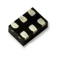


DSC1123DI2-050.0000
Timer, Oscillator & Pulse Generator, 50MHz, 2.25V to 3.63V, VDFN-6
- Manufacturer: MICROCHIP
- Product type: MEMS Oscillators
- Frequency:50MHz; Supply Voltage Min:2.25V; Supply Voltage Max:3.63V; No. of Pins:6Pins; Operating Temperature Min:-40°C; Operating Temperature Max:85°C; Product Range:-; MSL:MSL 1 - Unlimited;
- SVHC: No SVHC (04-Feb-2026)
- Frequency: 50MHz
- No. of Pins: 6Pins
- Frequency Nom: 50MHz
- Product Range: DSC1123 Series
- Supply Voltage Max: 3.63V
- Supply Voltage Min: 2.25V
- Supply Voltage Nom: 3.3V
- Frequency Stability + / -: 25ppm
- Operating Temperature Max: 85°C
- Operating Temperature Min: -40°C
- Oscillator Case / Package: SMD, 2.5mm x 2mm
- Oscillator Output Compatibility: LVDS
| Delivery and price | |
|---|---|
| Units per pack | 250 |
| Price | 0.87 € |
| Current stock | 10+ |
| Lead time | 30 days |
## **DSC1103/23** ~~MICROCHIP~~ ## **Low-Jitter Precision LVDS Oscillator** ## **Features** - Low RMS Phase Jitter: <1 ps (typ.) - High Stability: ±10 ppm, ±20 ppm, ±25 ppm, ±50 ppm - Wide Temperature Range: - Ext. Industrial –40°C to +105°C - Industrial –40°C to +85°C - Ext. Commercial –20°C to +70°C - High Supply Noise Rejection: –50 dBc - Wide Frequency Range: - 2.3 MHz – 460 MHz - Small Industry Standard Footprints - 2.5 mm x 2.0 mm - 3.2 mm x 2.5 mm - 5.0 mm x 3.2 mm ## **General Description** The DSC1103 and DSC1123 series of high performance oscillators utilizes a proven silicon MEMS technology to provide excellent jitter and stability over a wide range of supply voltages and temperatures. By eliminating the need for quartz or SAW technology, MEMS oscillators significantly enhance reliability and accelerate product development, while meeting stringent clock performance criteria for a variety of communications, storage, and networking applications. DSC1103 has a standby feature allowing it to completely power-down when EN pin is pulled low. For DSC1123, only the outputs are disabled when EN is low. Both oscillators are available in industry standard packages, including the smallest 2.5 mm x 2.0 mm, and are drop-in replacements for standard 6-pin LVDS crystal oscillators. - 7.0 mm x 5.0 mm - Excellent Shock and Vibration Immunity ## **Block Diagram** - Qualified to MIL-STD-883 - High Reliability - 20x better MTF than quartz-based devices - Low Current Consumption - Supply Range of 2.25V to 3.63V - Standby and Output Enable Functions - Lead Free and RoHS-Compliant ## **Applications** - Storage Area Networks **==> picture [199 x 89] intentionally omitted <==** **----- Start of picture text -----**<br> Pin 1 Pin 6<br>Enable Temp. Sensor & Compensation VDD<br>Circuitry<br>Pin 2 Pin 5<br>NC MEMS Divider Output<br>PLL<br>Oscillator Driver<br>ee ee<br>Pin 3 Pin 4<br>GND Output<br>**----- End of picture text -----**<br> - SATA, SAS, Fibre Channel - Passive Optical Networks - EPON, 10G-EPON, GPON, 10G-PON - HD/SD/SDI Video and Surveillance - PCI Express Gen 1/Gen 2/Gen 3 - Display Port DS20005745B-page 1 2017-2018 Microchip Technology Inc. **DSC1103/23** ## **1.0 ELECTRICAL CHARACTERISTICS** ## **Absolute Maximum Ratings †** Supply Voltage .......................................................................................................................................... –0.3V to +4.0V Input Voltage .......................................................................................................................................–0.3V to VDD+0.3V ESD Protection (HBM) ...............................................................................................................................................4 kV ESD Protection (MM) ................................................................................................................................................400V ESD Protection (CDM) ............................................................................................................................................1.5 kV **† Notice:** Stresses above those listed under “Absolute Maximum Ratings” may cause permanent damage to the device. This is a stress rating only and functional operation of the device at those or any other conditions above those indicated in the operational sections of this specification is not intended. Exposure to maximum rating conditions for extended periods may affect device reliability. ## **ELECTRICAL CHARACTERISTICS** Specifications: VDD = 3.3V; TA = +25°C unless otherwise specified. |**Parameters**|**Sym.**|**Min.**|**Typ.**|**Max.**|**Units**|**Conditions**| |---|---|---|---|---|---|---| |SupplyVoltage(Note 1)|VDD|2.25|—|3.63|V|—| |Supply Current|IDD|—|—|0.095|mA|DSC1103, EN pin low; all<br>outputs disabled.| |||—|20|22||DSC1123, EN pin low; all<br>outputs disabled.| |Frequency Stability|∆f|—|—|±10|ppm|Includes frequency<br>variations due to initial<br>tolerance, temp., and power<br>supply voltage.| |||—|—|±20||| |||—|—|±25||| |||—|—|±50||| |Aging- First Year|∆fY1|—|—|±5|ppm|Oneyear at +25°C| |Aging - After First Year|∆fY2+|—|—|<±1|ppm/yr|Year two and beyond at<br>+25°C| |Start-upTime(Note 2)|tSU|—|—|5|ms|T = +25°C| |Input Logic Levels|VIH|0.75 x VDD|—|—|V|Input logic high| ||VIL|—|—|0.25 x VDD||Input logic low| |Output Disable Time(Note 3)|tDA|—|—|5|ns|—| |Output Enable Time|tEN|—|—|5|ms|DSC1103| |||—|—|20|ns|DSC1123| |Enable Pull-Up Resistor<br>(Note 4)|RPU|—|40|—|kΩ|Pull-up resistor exist.| |**LVDS Outputs**||||||| |SupplyCurrent|IDD|—|29|32|mA|Output enabled, RL= 100Ω| |Output Offset Voltage|VOS|1.125|—|1.4|V|R = 100Ω Differential| |Delta Offset Voltage|∆VOS|—|—|50|mV|—| |Peak-to-Peak Output Swing|VPP|—|350|—|mV|Single-Ended| - **Note 1:** VDD pin should be filtered with a 0.1 µF capacitor. - **2:** tSU is time to 100 ppm stable output frequency after VDD is applied and outputs are enabled. - **3:** See the Output Waveform section and the Test Circuit for more information. - **4:** Output is enabled if pad is floated or not connected. DS20005745B-page 2 2017-2018 Microchip Technology Inc. **DSC1103/23** ## **ELECTRICAL CHARACTERISTICS (CONTINUED)** Specifications: VDD = 3.3V; TA = +25°C unless otherwise specified. |**Parameters**|**Sym.**|**Min.**|**Typ.**|**Max.**|**Units**|**Conditions**| |---|---|---|---|---|---|---| |Output Transition Rise/Fall<br>Time(Note 3)|tR/tF|—|200|—|ps|20% to 80%<br>RL= 50Ω, CL= 2pF| |Frequency|f0|2.3|—|460|MHz|–20°C to +70°C &<br>–40°C to +85°C| |||3.3|—|460||–40°C to +105°C| |Output DutyCycle|SYM|48|—|52|%|Differential| |Period Jitter|JPER|—|2.5|—|psRMS|—| |Integrated Phase Noise|JPH|—|0.28|—|psRMS|200 kHz to 20 MHz<br>@156.25 MHz| |||—|0.4|—||100 kHz to 20 MHz<br>@156.25 MHz| |||—|1.7|2||12 kHz to 20 MHz<br>@156.25 MHz| - **Note 1:** VDD pin should be filtered with a 0.1 µF capacitor. - **2:** tSU is time to 100 ppm stable output frequency after VDD is applied and outputs are enabled. - **3:** See the Output Waveform section and the Test Circuit for more information. - **4:** Output is enabled if pad is floated or not connected. DS20005745B-page 3 2017-2018 Microchip Technology Inc. **DSC1103/23** ## **TEMPERATURE SPECIFICATIONS (Note 1)** |**Parameters**|**Sym.**|**Min.**|**Typ.**|**Max.**|**Units**|**Conditions**| |---|---|---|---|---|---|---| |**Temperature Ranges**||||||| |Operating Temperature Range|TA|–20|—|+70|°C|OrderingOption E| ||TA|–40|—|+85|°C|OrderingOption I| ||TA|–40|—|+105|°C|OrderingOption L| |Junction Temperature|TJ|—|—|+150|°C|—| |Storage Temperature Range|TS|–55|—|+150|°C|—| |SolderingTemperature|—|—|—|+260|°C|40 sec. max.| **Note 1:** The maximum allowable power dissipation is a function of ambient temperature, the maximum allowable junction temperature, and the thermal resistance from junction to air (i.e., TA, TJ, JA). Exceeding the maximum allowable power dissipation will cause the device operating junction temperature to exceed the maximum +150°C rating. Sustained junction temperatures above +150°C can impact the device reliability. DS20005745B-page 4 2017-2018 Microchip Technology Inc. **DSC1103/23** ## **2.0 PIN DESCRIPTIONS** The descriptions of the pins are listed in Table 2-1. ## **TABLE 2-1: PIN FUNCTION TABLE** |**Pin Number**<br>**7x5 with Pad**|**Pin Number**<br>**7x5 w/o Pad**|**Pin Number**<br>**5x3.2**|**Pin Number**<br>**3.2x2.5**|**Pin Number**<br>**2x2.5**|**Pin**<br>**Name**|**Description**| |---|---|---|---|---|---|---| |1|1|1|1|1|EN|Enable| |2|2|2|2|2|NC|Do not connect| |3|3|3|3|3|GND|Ground| |4|4|4|4|4|OUT|LVDS clock output +| |5|5|5|5|5|OUT–|LVDS clock output –| |6|6|6|6|6|VDD|Supplyvoltage| |PAD|—|—|—|—|PAD|Tie to Ground| ## **TABLE 2-2: OUTPUT ENABLE MODES** |**EN Pin**|**DSC1103**|**DSC1123**| |---|---|---| |High|Outputs Active|Outputs Active| |NC|Outputs Active|Outputs Active| |Low|Standby|Outputs Disabled| DS20005745B-page 5 2017-2018 Microchip Technology Inc. **DSC1103/23** ## **3.0 NOMINAL PERFORMANCE PARAMETERS** Unless otherwise specified, T = +25°C, VDD = 3.3V. **==> picture [216 x 144] intentionally omitted <==** **----- Start of picture text -----**<br> 0<br>50 mV<br>-10<br>100 mV<br>-20<br>-30<br>-40<br>-50<br>-60<br>-70<br>-80<br>0.1 1 10 100 1000 10000<br>Supply Noise Frequency (kHz)<br>Rejection (dBc)<br>**----- End of picture text -----**<br> _**FIGURE 3-1:** Power Supply Rejection Ratio._ **==> picture [216 x 145] intentionally omitted <==** **----- Start of picture text -----**<br> 2.5<br>156MHz-LVDS<br>2.0 212MHz-LVDS<br>320MHz-LVDS<br>1.5 410MHz-LVDS<br>1.0<br>0.5<br>0.0<br>0 200 400 600 800 1000<br>Low-end of integration BW: x kHz to 20 MHz<br>Phase Jitter (ps RMS)<br>**----- End of picture text -----**<br> _**FIGURE 3-2:** Phase Jitter (Integrated Phase Noise)._ DS20005745B-page 6 2017-2018 Microchip Technology Inc. **DSC1103/23** ## **4.0 TERMINATION SCHEME** **==> picture [276 x 158] intentionally omitted <==** **----- Start of picture text -----**<br> VDD<br>0.1uF<br>6<br>2 5<br>100 � 100 �<br>3 4<br>**----- End of picture text -----**<br> _**FIGURE 4-1:** Typical Termination Scheme._ ## **5.0 OUTPUT WAVEFORM** **==> picture [418 x 177] intentionally omitted <==** **----- Start of picture text -----**<br> tR tF<br>Output 80%<br>50% 830 mv350 mV<br>20%<br>Output<br>1/f o tEN<br>tDA<br>VIH<br>Enable<br>VIL<br>**----- End of picture text -----**<br> _**FIGURE 5-1:** Output Waveform._ DS20005745B-page 7 2017-2018 Microchip Technology Inc. **DSC1103/23** ## **6.0 TEST CIRCUIT** _**FIGURE 6-1:** Test Circuit._ ## **7.0 RECOMMENDED BOARD LAYOUT** **==> picture [308 x 187] intentionally omitted <==** **----- Start of picture text -----**<br> Via to GND layer<br>1 6<br>Supply bypass<br>capacitor<br>2 5<br>3 4<br>Via to GND layer<br>**----- End of picture text -----**<br> _**FIGURE 7-1:** DSC1103/23 Recommended Board Layout._ DS20005745B-page 8 2017-2018 Microchip Technology Inc. **DSC1103/23** ## **8.0 SOLDER REFLOW PROFILE** **==> picture [264 x 136] intentionally omitted <==** **----- Start of picture text -----**<br> 20-40<br>° Sec<br>260 C<br>217°C<br>60-150<br>200°C Sec<br>° 60-180 Re�ow<br>150 C<br>Sec<br>Pre heat Cool<br>25°C<br>8 min max Time<br>°C/Sec Max.<br>3<br>°C/Sec Max.<br>3<br>6°<br>C/Sec Max.<br>°C)<br>Temperature (<br>**----- End of picture text -----**<br> |**MSL 1 @ 260°C refer to JSTD-020C**|**MSL 1 @ 260°C refer to JSTD-020C**| |---|---| |Ramp-UpRate(200°C to Peak Temp)|3°C/sec. max.| |Preheat Time 150°C to 200°C|60-180 sec.| |Time Maintained above 217°C|60-150 sec.| |Peak Temperature|255°C to 260°C| |Time within 5°C of Actual Peak|20-40 sec.| |Ramp-Down Rate|6°C/sec. max.| |Time 25°C to Peak Temperature|8 minutes max.| DS20005745B-page 9 2017-2018 Microchip Technology Inc. **DSC1103/23** ## **9.0 PACKAGE MARKING INFORMATION** ## **6-Lead VDFN 2.5 mm x 2.0 mm Package Outline and Recommended Land Pattern** ## **6-Lead Very Thin Dual Flatpack No-Leads (J7A) - 2.5x2.0 mm Body [VDFN]** **==> picture [417 x 290] intentionally omitted <==** **----- Start of picture text -----**<br> Note: For the most current package drawings, please see the Microchip Packaging Specification located at<br>http://www.microchip.com/packaging<br>X1<br>X2<br>1 2<br>Y<br>G2 C<br>6<br>G1 SILK SCREEN<br>E<br>**----- End of picture text -----**<br> **==> picture [170 x 9] intentionally omitted <==** **----- Start of picture text -----**<br> RECOMMENDED LAND PATTERN<br>**----- End of picture text -----**<br> ||||Units|MILLIMETERS|MILLIMETERS|MILLIMETERS|| |---|---|---|---|---|---|---|---| |||Dimension|Limits|MIN|NOM|MAX|| |||Contact Pitch|E||0.825 BSC||| |||Contact Pad Width(X4)|X1|||0.65|| |||Contact Pad Width(X2)|X2|||0.25|| |||Contact Pad Length(X6)|Y|||0.85|| |||Contact Pad Spacing|C||1.45||| |||Space Between Contacts(X4)|G1|0.38|||| |||Space Between Contacts(X3)|G2|0.60|||| |Notes:|||||||| |1.|Dimensioning and tolerancing per ASME Y14.5M||||||| ||BSC: Basic Dimension. Theoretically exact value shown without tolerances.||||||| |2.|For best soldering results, thermal vias, if used, should be filled or tented to avoid solder loss during||||||| ||reflow process||||||| |||||Microchip Technology Drawing C04-3005A|||| DS20005745B-page 10 2017-2018 Microchip Technology Inc. **DSC1103/23** ## **6-Lead Very Thin Dual Flatpack No-Leads (J7A) - 2.5x2.0 mm Body [VDFN]** **Note:** For the most current package drawings, please see the Microchip Packaging Specification located at http://www.microchip.com/packaging **==> picture [312 x 455] intentionally omitted <==** **----- Start of picture text -----**<br> D A<br>B<br>N<br>(DATUM A)<br>(DATUM B)<br>E<br>NOTE 1<br>2X<br>0.05 C<br>1 2<br>2X<br>TOP VIEW<br>0.05 C<br>0.10 C<br>C A<br>A1<br>SEATING<br>PLANE<br>6X<br>SIDE VIEW 0.08 C<br>2X b2<br>1 2<br>L2<br>5X L1<br>N<br>4X b1<br>e 0.10 C A B<br>0.05 C<br>BOTTOM VIEW<br>**----- End of picture text -----**<br> Microchip Technology Drawing C04-1005A Sheet 1 of 2 DS20005745B-page 11 2017-2018 Microchip Technology Inc. **DSC1103/23** ## **6-Lead Very Thin Dual Flatpack No-Leads (J7A) - 2.5x2.0 mm Body [VDFN]** **Note:** For the most current package drawings, please see the Microchip Packaging Specification located at http://www.microchip.com/packaging **==> picture [213 x 183] intentionally omitted <==** ## Notes: |Units|Units|MILLIMETERS|MILLIMETERS|MILLIMETERS| |---|---|---|---|---| |Dimension Limits||MIN|NOM|MAX| |Number of Terminals|N|6||| |Pitch|e|0.825 BSC||| |Overall Height|A|0.80|0.85|0.90| |Standoff|A1|0.00|0.02|0.05| |Overall Length|D|2.50 BSC||| |Overall Width|E|2.00 BSC||| |Terminal Width|b1|0.60|0.65|0.70| |Terminal Width|b2|0.20|0.25|0.30| |Terminal Length|L1|0.60|0.70|0.80| |Terminal Length|L2|0.665|0.765|0.865| 1. Pin 1 visual index feature may vary, but must be located within the hatched area. 2. Package is saw singulated 3. Dimensioning and tolerancing per ASME Y14.5M - BSC: Basic Dimension. Theoretically exact value shown without tolerances. - REF: Reference Dimension, usually without tolerance, for information purposes only. Microchip Technology Drawing C04-1005A Sheet 2 of 2 DS20005745B-page 12 2017-2018 Microchip Technology Inc. **DSC1103/23** ## **6-Lead VDFN 3.2 mm x 2.5 mm Package Outline and Recommended Land Pattern** ## **6-Lead Very Thin Plastic Dual Flatpack No-Lead (H5A) - 3.2x2.5 mm Body [VDFN]** **==> picture [418 x 278] intentionally omitted <==** **----- Start of picture text -----**<br> Note: For the most current package drawings, please see the Microchip Packaging Specification located at<br>http://www.microchip.com/packaging<br>X2<br>G<br>6<br>C<br>Y<br>1 2<br>X1 SILK SCREEN<br>E<br>**----- End of picture text -----**<br> ## RECOMMENDED LAND PATTERN |Units|Units|MILLIMETERS|MILLIMETERS|MILLIMETERS| |---|---|---|---|---| |Dimension Limits||MIN|NOM|MAX| |Contact Pitch|E|1.05 BSC||| |Contact Pad Spacing|C||1.60|| |Contact Pad Width(X4)|X1|||1.00| |Contact Pad Width(X2)|X2|||0.60| |Contact Pad Length(X6)|Y|||0.85| |Space Between Contacts(X4)|G1|0.25||| ## Notes: 1. Dimensioning and tolerancing per ASME Y14.5M BSC: Basic Dimension. Theoretically exact value shown without tolerances. Microchip Technology Drawing C04-3007A DS20005745B-page 13 2017-2018 Microchip Technology Inc. **DSC1103/23** ## **6-Lead Very Thin Plastic Dual Flatpack No-Lead (H5A) - 3.2x2.5 mm Body [VDFN]** **==> picture [417 x 499] intentionally omitted <==** **----- Start of picture text -----**<br> Note: For the most current package drawings, please see the Microchip Packaging Specification located at<br>http://www.microchip.com/packaging<br>D A<br>B<br>N<br>(DATUM A)<br>(DATUM B)<br>E<br>NOTE 1<br>2X<br>0.05 C<br>1 2<br>2X<br>0.05 C TOP VIEW<br>0.10 C A1<br>C<br>A<br>SEATING<br>PLANE<br>6X<br>0.08 C<br>SIDE VIEW<br>2X b2<br>1 2<br>NOTE 1<br>L<br>N<br>4X b1<br>L1<br>e 0.07 C A B<br>0.05 C<br>BOTTOM VIEW<br>**----- End of picture text -----**<br> **==> picture [194 x 8] intentionally omitted <==** **----- Start of picture text -----**<br> Microchip Technology Drawing C04-1007A Sheet 1 of 2<br>**----- End of picture text -----**<br> DS20005745B-page 14 2017-2018 Microchip Technology Inc. **DSC1103/23** ## **6-Lead Very Thin Plastic Dual Flatpack No-Lead (H5A) - 3.2x2.5 mm Body [VDFN]** **Note:** For the most current package drawings, please see the Microchip Packaging Specification located at http://www.microchip.com/packaging **==> picture [214 x 182] intentionally omitted <==** |Units|Units|MILLIMETERS|MILLIMETERS|MILLIMETERS| |---|---|---|---|---| |Dimension Limits||MIN|NOM|MAX| |Number of Terminals|N|6||| |Pitch|e|1.05 BSC||| |Overall Height|A|0.80|0.85|0.90| |Standoff|A1|0.00|0.02|0.05| |Overall Length|D|3.20 BSC||| |Overall Width|E|2.50 BSC||| |Terminal Width|b1|0.85|0.90|0.95| |Terminal Width|b2|0.45|0.50|0.55| |Terminal Length|L|0.65|0.70|0.75| |Terminal Pullback|L1|0.10 REF||| Notes: 1. Pin 1 visual index feature may vary, but must be located within the hatched area. 2. Package is saw singulated 3. Dimensioning and tolerancing per ASME Y14.5M BSC: Basic Dimension. Theoretically exact value shown without tolerances. REF: Reference Dimension, usually without tolerance, for information purposes only. Microchip Technology Drawing C04-1007A Sheet 2 of 2 DS20005745B-page 15 2017-2018 Microchip Technology Inc. **DSC1103/23** ## **6-Lead CDFN 5.0 mm x 3.2 mm Package Outline and Recommended Land Pattern** DS20005745B-page 16 2017-2018 Microchip Technology Inc. **DSC1103/23** ## **6-Lead VDFN 7.0 mm x 5.0 mm Package Outline and Recommended Land Pattern** ## **6-Lead Very Thin Plastic Quad Flat, No Lead Package (H8A) - 7x5 mm Body [VDFN] With 2.8x1.8 mm Exposed Pad** **==> picture [417 x 272] intentionally omitted <==** **----- Start of picture text -----**<br> Note: For the most current package drawings, please see the Microchip Packaging Specification located at<br>http://www.microchip.com/packaging<br>X2<br>EV<br>6<br>C Y2 EV ØV<br>G<br>Y1<br>1 2<br>X1<br>E<br>SILK SCREEN<br>**----- End of picture text -----**<br> ## RECOMMENDED LAND PATTERN |Units|Units|MILLIMETERS|MILLIMETERS|MILLIMETERS| |---|---|---|---|---| |Dimension Limits||MIN|NOM|MAX| |Contact Pitch|E|2.54 BSC||| |Optional Center Pad Width|X2|||2.90| |Optional Center Pad Length|Y2|||1.90| |Contact Pad Spacing|C||3.70|| |Contact Pad Width(X6)|X1|||1.50| |Contact Pad Length(X6)|Y1|||1.35| |Contact Pad to Center Pad(X2)|G|0.20||| |Thermal Via Diameter(X6)|V||0.33|| |Thermal Via Pitch|EV||1.20|| Notes: 1. Dimensioning and tolerancing per ASME Y14.5M BSC: Basic Dimension. Theoretically exact value shown without tolerances. 2. For best soldering results, thermal vias, if used, should be filled or tented to avoid solder loss during reflow process Microchip Technology Drawing C04-3010A DS20005745B-page 17 2017-2018 Microchip Technology Inc. **DSC1103/23** ## **6-Lead Very Thin Plastic Quad Flat, No Lead Package (H8A) - 7x5 mm Body [VDFN] With 2.8x1.8 mm Exposed Pad** **==> picture [415 x 514] intentionally omitted <==** **----- Start of picture text -----**<br> Note: For the most current package drawings, please see the Microchip Packaging Specification located at<br>http://www.microchip.com/packaging<br>D A<br>B<br>N<br>(DATUM A)<br>(DATUM B)<br>E<br>NOTE 1<br>2X<br>0.20 C<br>1 2<br>2X<br>0.20 C<br>TOP VIEW<br>A1<br>0.10 C<br>C<br>A<br>SEATING<br>PLANE<br>6X<br>0.08 C<br>SIDE VIEW<br>0.10 C A B<br>D2<br>1 2<br>0.10 C A B<br>NOTE 1<br>E2<br>6X L<br>(K)<br>N<br>6X b<br>e 0.10 C A B<br>0.05 C<br>BOTTOM VIEW<br>**----- End of picture text -----**<br> Microchip Technology Drawing C04-1010A Sheet 1 of 2 DS20005745B-page 18 2017-2018 Microchip Technology Inc. **DSC1103/23** ## **6-Lead Very Thin Plastic Quad Flat, No Lead Package (H8A) - 7x5 mm Body [VDFN] With 2.8x1.8 mm Exposed Pad** **Note:** For the most current package drawings, please see the Microchip Packaging Specification located at http://www.microchip.com/packaging **==> picture [194 x 112] intentionally omitted <==** ## Notes: |Units|Units|MILLIMETERS|MILLIMETERS|MILLIMETERS| |---|---|---|---|---| |Dimension Limits||MIN|NOM|MAX| |Number of Terminals|N|6||| |Pitch|e|2.54||| |Overall Height|A|0.80|0.85|0.90| |Standoff|A1|0.00|0.02|0.05| |Overall Length|D|7.00 BSC||| |Exposed Pad Length|D2|2.70|2.80|2.90| |Overall Width|E|5.00 BSC||| |Exposed Pad Width|E2|1.70|1.80|1.90| |Terminal Width|b|1.35|1.40|1.45| |Terminal Length|L|1.00|1.10|1.20| |Terminal-to-Exposed-Pad|K|0.20 REF||| 1. Pin 1 visual index feature may vary, but must be located within the hatched area. 2. Package is saw singulated 3. Dimensioning and tolerancing per ASME Y14.5M - BSC: Basic Dimension. Theoretically exact value shown without tolerances. - REF: Reference Dimension, usually without tolerance, for information purposes only. Microchip Technology Drawing C04-1010A Sheet 2 of 2 DS20005745B-page 19 2017-2018 Microchip Technology Inc. **DSC1103/23** ## **6-Lead CDFN 7.0 mm x 5.0 mm Package Outline and Recommended Land Pattern** DS20005745B-page 20 2017-2018 Microchip Technology Inc. **DSC1103/23** ## **APPENDIX A: REVISION HISTORY** ## **Revision A (March 2017)** - Converted Micrel data sheet DSC1103/23 to Microchip DS20005745A. - Minor text changes throughout. - Updated Package Marking Information to MCHPstandard drawings where available. ## **Revision B (October 2018)** - Added ±20 ppm stability references throughout document. - Added Section 7.0, Recommended Board Layout. DS20005745B-page 21 2017-2018 Microchip Technology Inc. **DSC1103/23** ## **NOTES:** DS20005745B-page 22 2017-2018 Microchip Technology Inc. **DSC1103/23** ## **PRODUCT IDENTIFICATION SYSTEM** To order or obtain information, e.g., on pricing or delivery, contact your local Microchip representative or sales office. |**PART NO.**|**PART NO.**|**PART NO.**|**X**|**X**|**3**|**3**|**X**<br>**X**<br>**X**|**X**<br>**X**<br>**X**|**X**<br>**X**<br>**X**|**xxx.xxxx**|**xxx.xxxx**|**X**|**X**||**Examples:**|**Examples:**|| |---|---|---|---|---|---|---|---|---|---|---|---|---|---|---|---|---|---| ||||||||||||||||a) DSC1103AE1-125.0000: Low-Jitter Precision LVDS||| |**Device**||**Enable**|||**Device**||**Package**<br>**Temp.**<br>**Stability**|||**Frequency**||**Packing**||||Oscillator, Enable/Standby,|| |**(First 2**||**Modes**|||**(Last**|||**Range**||||||||7x5 VDFN, –20°C to +70°C,|| |**Digits)**|||||**Digit)**|||||||||||±50 ppm, 125 MHz, 100/Tube|| |**Device:**|||||DSC11x3:|||Low-Jitter Precision LVDS Oscillator|||||||b) DSC1123BI2-400.0000T: Low-Jitter Precision LVDS<br>Oscillator, Enable/Disable,||| |||||||||||||||||5x3.2 CDFN, –40°C to +85°C,|| |**Enable Modes:**|||||0||=|Enable/Standby||||||||±25 ppm, 400 MHz,|| ||||||2||=|Enable/Disable||||||||1,000/Reel|| ||||||||||||||||c) DSC1103CL5-074.2500: Low-Jitter Precision LVDS||| |**Package:**|||||A||=|7.0 mm x 5.0 mm VDFN||||||||Oscillator, Enable/Standby,|| ||||||B||=|5.0 mm x 3.2 mm CDFN||||||||3.2x2.5 VDFN,|| ||||||C<br>D<br>N||=<br>=<br>=|3.2 mm x 2.5 mm VDFN<br>2.5 mm x 2.0 mm VDFN<br>7.0 mm x 5.0 mm CDFN (no center pad)||||||||–40°C to +105°C, ±10 ppm,<br>74.25 MHz, 100/Tube|| ||||||||||||||||d) DSC1123DE1-082.5000T:Low-Jitter Precision LVDS||| |||||||||||||||||Oscillator, Enable/Disable,|| |**Temperature**<br>**Range:**|||||E<br>I<br>L||=<br>=<br>=|–20°C to +70°C<br>–40°C to +85°C<br>–40°C to +105°C||||||||2.5x2.0 VDFN,<br>–20°C to +70°C, ±50 ppm,|| |||||||||||||||||82.5 MHz, 1,000/Reel|| |**Stability:**|||||1<br>2<br>3||=<br>=<br>=|±50 ppm<br>±25 ppm<br>±20 ppm|||||||e) DSC1103NI2-056.0000: Low-Jitter Precision LVDS<br>Oscillator, Enable/Standby,<br>7x5 CDFN (no center pad),||| ||||||5||=|±10 ppm||||||||–40°C to +85°C, ±25 ppm,|| |||||||||||||||||56 MHz, 100/Tube|| |**Frequency Code:**|||||xxx.xxxx =|||2.3 MHz to 460 MHz (user-defined)|||||||**Note 1:**|Tape and Reel identifier only appears in the|| |||||||||||||||||catalog part number description. This identifier is|| |**Packing:**|||||T<br>=<br>(blank) =|||1,000/Reel<br>100/Tube||||||||used for ordering purposes and is not printed on<br>the device package. Check with your Microchip<br>Sales Office for package availability with the|| |||||||||||||||||Tape and Reel option.|| DS20005745B-page 23 2017-2018 Microchip Technology Inc. **DSC1103/23** ## **NOTES:** DS20005745B-page 24 2017-2018 Microchip Technology Inc. ## **Note the following details of the code protection feature on Microchip devices:** - Microchip products meet the specification contained in their particular Microchip Data Sheet. - Microchip believes that its family of products is one of the most secure families of its kind on the market today, when used in the intended manner and under normal conditions. - There are dishonest and possibly illegal methods used to breach the code protection feature. All of these methods, to our knowledge, require using the Microchip products in a manner outside the operating specifications contained in Microchip’s Data Sheets. Most likely, the person doing so is engaged in theft of intellectual property. - Microchip is willing to work with the customer who is concerned about the integrity of their code. - Neither Microchip nor any other semiconductor manufacturer can guarantee the security of their code. Code protection does not mean that we are guaranteeing the product as “unbreakable.” Code protection is constantly evolving. We at Microchip are committed to continuously improving the code protection features of our products. Attempts to break Microchip’s code protection feature may be a violation of the Digital Millennium Copyright Act. If such acts allow unauthorized access to your software or other copyrighted work, you may have a right to sue for relief under that Act. Information contained in this publication regarding device applications and the like is provided only for your convenience and may be superseded by updates. It is your responsibility to ensure that your application meets with your specifications. MICROCHIP MAKES NO REPRESENTATIONS OR WARRANTIES OF ANY KIND WHETHER EXPRESS OR IMPLIED, WRITTEN OR ORAL, STATUTORY OR OTHERWISE, RELATED TO THE INFORMATION, INCLUDING BUT NOT LIMITED TO ITS CONDITION, QUALITY, PERFORMANCE, MERCHANTABILITY OR FITNESS FOR PURPOSE **.** Microchip disclaims all liability arising from this information and its use. Use of Microchip devices in life support and/or safety applications is entirely at the buyer’s risk, and the buyer agrees to defend, indemnify and hold harmless Microchip from any and all damages, claims, suits, or expenses resulting from such use. No licenses are conveyed, implicitly or otherwise, under any Microchip intellectual property rights unless otherwise stated. _Microchip received ISO/TS-16949:2009 certification for its worldwide headquarters, design and wafer fabrication facilities in Chandler and Tempe, Arizona; Gresham, Oregon and design centers in California and India. The Company’s quality system processes and procedures are for its PIC[®] MCUs and dsPIC[®] DSCs, KEELOQ[®] code hopping devices, Serial EEPROMs, microperipherals, nonvolatile memory and analog products. In addition, Microchip’s quality system for the design and manufacture of development systems is ISO 9001:2000 certified._ ## **QUALITY MANAGEMENT SYSTEM** ## **CERTIFIED BY DNV** ## == == **ISO/TS 16949** ## **Trademarks** The Microchip name and logo, the Microchip logo, AnyRate, AVR, AVR logo, AVR Freaks, BitCloud, chipKIT, chipKIT logo, CryptoMemory, CryptoRF, dsPIC, FlashFlex, flexPWR, Heldo, JukeBlox, KeeLoq, Kleer, LANCheck, LINK MD, maXStylus, maXTouch, MediaLB, megaAVR, MOST, MOST logo, MPLAB, OptoLyzer, PIC, picoPower, PICSTART, PIC32 logo, Prochip Designer, QTouch, SAM-BA, SpyNIC, SST, SST Logo, SuperFlash, tinyAVR, UNI/O, and XMEGA are registered trademarks of Microchip Technology Incorporated in the U.S.A. and other countries. ClockWorks, The Embedded Control Solutions Company, EtherSynch, Hyper Speed Control, HyperLight Load, IntelliMOS, mTouch, Precision Edge, and Quiet-Wire are registered trademarks of Microchip Technology Incorporated in the U.S.A. Adjacent Key Suppression, AKS, Analog-for-the-Digital Age, Any Capacitor, AnyIn, AnyOut, BodyCom, CodeGuard, CryptoAuthentication, CryptoAutomotive, CryptoCompanion, CryptoController, dsPICDEM, dsPICDEM.net, Dynamic Average Matching, DAM, ECAN, EtherGREEN, In-Circuit Serial Programming, ICSP, INICnet, Inter-Chip Connectivity, JitterBlocker, KleerNet, KleerNet logo, memBrain, Mindi, MiWi, motorBench, MPASM, MPF, MPLAB Certified logo, MPLIB, MPLINK, MultiTRAK, NetDetach, Omniscient Code Generation, PICDEM, PICDEM.net, PICkit, PICtail, PowerSmart, PureSilicon, QMatrix, REAL ICE, Ripple Blocker, SAM-ICE, Serial Quad I/O, SMART-I.S., SQI, SuperSwitcher, SuperSwitcher II, Total Endurance, TSHARC, USBCheck, VariSense, ViewSpan, WiperLock, Wireless DNA, and ZENA are trademarks of Microchip Technology Incorporated in the U.S.A. and other countries. SQTP is a service mark of Microchip Technology Incorporated in the U.S.A. Silicon Storage Technology is a registered trademark of Microchip Technology Inc. in other countries. GestIC is a registered trademark of Microchip Technology Germany II GmbH & Co. KG, a subsidiary of Microchip Technology Inc., in other countries. All other trademarks mentioned herein are property of their respective companies. - © 2017-2018, Microchip Technology Incorporated, All Rights Reserved. ISBN: 978-1-5224-3790-1 DS20005745B-page 25 2017-2018 Microchip Technology Inc. ## **Worldwide Sales and Service** ## **AMERICAS** **Corporate Office** 2355 West Chandler Blvd. Chandler, AZ 85224-6199 Tel: 480-792-7200 Fax: 480-792-7277 Technical Support: http://www.microchip.com/ support Web Address: www.microchip.com **Atlanta** Duluth, GA Tel: 678-957-9614 Fax: 678-957-1455 **Austin, TX** Tel: 512-257-3370 **Boston** Westborough, MA Tel: 774-760-0087 Fax: 774-760-0088 **Chicago** Itasca, IL Tel: 630-285-0071 Fax: 630-285-0075 **Dallas** Addison, TX Tel: 972-818-7423 Fax: 972-818-2924 **Detroit** Novi, MI Tel: 248-848-4000 **Houston, TX** Tel: 281-894-5983 **Indianapolis** Noblesville, IN Tel: 317-773-8323 Fax: 317-773-5453 Tel: 317-536-2380 **Los Angeles** Mission Viejo, CA Tel: 949-462-9523 Fax: 949-462-9608 Tel: 951-273-7800 **Raleigh, NC** Tel: 919-844-7510 **New York, NY** Tel: 631-435-6000 **San Jose, CA** Tel: 408-735-9110 Tel: 408-436-4270 **Canada - Toronto** Tel: 905-695-1980 Fax: 905-695-2078 ## **ASIA/PACIFIC** **Australia - Sydney** Tel: 61-2-9868-6733 **China - Beijing** Tel: 86-10-8569-7000 **China - Chengdu** Tel: 86-28-8665-5511 **China - Chongqing** Tel: 86-23-8980-9588 **China - Dongguan** Tel: 86-769-8702-9880 **China - Guangzhou** Tel: 86-20-8755-8029 **China - Hangzhou** Tel: 86-571-8792-8115 **China - Hong Kong SAR** Tel: 852-2943-5100 **China - Nanjing** Tel: 86-25-8473-2460 **China - Qingdao** Tel: 86-532-8502-7355 **China - Shanghai** Tel: 86-21-3326-8000 **China - Shenyang** Tel: 86-24-2334-2829 **China - Shenzhen** Tel: 86-755-8864-2200 **China - Suzhou** Tel: 86-186-6233-1526 **China - Wuhan** Tel: 86-27-5980-5300 **China - Xian** Tel: 86-29-8833-7252 **China - Xiamen** Tel: 86-592-2388138 **China - Zhuhai** Tel: 86-756-3210040 ## **ASIA/PACIFIC** **India - Bangalore** Tel: 91-80-3090-4444 **India - New Delhi** Tel: 91-11-4160-8631 **India - Pune** Tel: 91-20-4121-0141 **Japan - Osaka** Tel: 81-6-6152-7160 **Japan - Tokyo** Tel: 81-3-6880- 3770 **Korea - Daegu** Tel: 82-53-744-4301 **Korea - Seoul** Tel: 82-2-554-7200 **Malaysia - Kuala Lumpur** Tel: 60-3-7651-7906 **Malaysia - Penang** Tel: 60-4-227-8870 **Philippines - Manila** Tel: 63-2-634-9065 **Singapore** Tel: 65-6334-8870 **Taiwan - Hsin Chu** Tel: 886-3-577-8366 **Taiwan - Kaohsiung** Tel: 886-7-213-7830 **Taiwan - Taipei** Tel: 886-2-2508-8600 **Thailand - Bangkok** Tel: 66-2-694-1351 **Vietnam - Ho Chi Minh** Tel: 84-28-5448-2100 ## **EUROPE** **Austria - Wels** Tel: 43-7242-2244-39 Fax: 43-7242-2244-393 **Denmark - Copenhagen** Tel: 45-4450-2828 Fax: 45-4485-2829 **Finland - Espoo** Tel: 358-9-4520-820 **France - Paris** Tel: 33-1-69-53-63-20 Fax: 33-1-69-30-90-79 **Germany - Garching** Tel: 49-8931-9700 **Germany - Haan** Tel: 49-2129-3766400 **Germany - Heilbronn** Tel: 49-7131-67-3636 **Germany - Karlsruhe** Tel: 49-721-625370 **Germany - Munich** Tel: 49-89-627-144-0 Fax: 49-89-627-144-44 **Germany - Rosenheim** Tel: 49-8031-354-560 **Israel - Ra’anana** Tel: 972-9-744-7705 **Italy - Milan** Tel: 39-0331-742611 Fax: 39-0331-466781 **Italy - Padova** Tel: 39-049-7625286 **Netherlands - Drunen** Tel: 31-416-690399 Fax: 31-416-690340 **Norway - Trondheim** Tel: 47-7288-4388 **Poland - Warsaw** Tel: 48-22-3325737 **Romania - Bucharest** Tel: 40-21-407-87-50 **Spain - Madrid** Tel: 34-91-708-08-90 Fax: 34-91-708-08-91 **Sweden - Gothenberg** Tel: 46-31-704-60-40 **Sweden - Stockholm** Tel: 46-8-5090-4654 **UK - Wokingham** Tel: 44-118-921-5800 Fax: 44-118-921-5820 DS20005745B-page 26 2017-2018 Microchip Technology Inc. 08/15/18
Updated at April 29, 2026
Microchip Technology Inc. is a leading global provider of smart, connected, and secure embedded control solutions. Known for enabling engineers to design with confidence, the company delivers a comprehensive product portfolio that reduces total system costs and accelerates time to market across the industrial, automotive, communications, and computing sectors. Our extensive selection of Microchip components highlights the manufacturer's strength in both discrete semiconductors and advanced wireless connectivity. We carry a robust lineup of highly efficient single MOSFETs and Schottky diodes tailored for demanding power management and switching applications. Alongside these essential discretes, engineers can source a wide array of ready-to-use networking modules, prominently featuring Bluetooth and WLAN adapters that streamline the development of modern IoT and connected devices. Rounding out the offering is a diverse range of Microchip integrated circuits and specialized components. This includes versatile I/O expanders for simplified system integration, precision timing solutions such as MEMS oscillators and pulse generators, as well as AC/DC LED driver ICs and sub-2.4GHz RF transceivers. Backed by Microchip's renowned commitment to exceptional quality and reliable performance, these components provide scalable, dependable building blocks for complex electronic designs.
About Novapart
Novapart is a B2B electronic component broker specialising in stock shortages and cost reduction. We source hard-to-find parts and identify compliant alternatives across a catalogue of 410,000+ components from 500+ manufacturers.
Learn more →Stock Shortage Specialist
When a component is unavailable, discontinued or has an unacceptable lead time, we tap into our network of vetted European and Asian distributors to source what you need — without compromising on quality or traceability.
Request a quote →Compliant Alternatives
We identify pin-to-pin, electrically equivalent substitutes that meet the same certifications (RoHS, AEC-Q100, REACH) as your original specification — validated against datasheets, not just part numbers. Often at a lower cost.
BOM Analysis service →