
Image not available
Illustrative purposes only

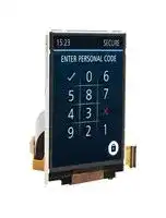
DMT028QVNTNT0S-1A
TFT LCD, 2.8
⚠️ Reference pricing provided. In case of supply shortages, we will connect you with our trusted procurement partners to ensure your project's continuity.
- Manufacturer: DENSITRON
- Product type: TFT LCD Displays
- Resolution: 240 x 320 Pixels
- Module Size: 49mm x 69mm
- Touchscreen: No Touchscreen
- Display Size: 2.8"
- Logic Voltage: 2.8V
- Interface Type: Parallel
- Display Appearance: RGB
- Display Brightness: 500cd/m²
- Display Orientation: Portrait
- Operating Temperature Max: 70°C
- Operating Temperature Min: -20°C
| Delivery and price | |
|---|---|
| Units per pack | 50 |
| Price | 20.1 € |
| Current stock | 10+ |
| Lead time | 30 days |
Datasheet

## **LIQUID CRYSTAL DISPLAY MODULE** ## **Product Specification** **CUSTOMER CUSTOMER PART NUMBER PRODUCT NUMBER DMT028QVNTNT0S-1A** **==> picture [265 x 76] intentionally omitted <==** **----- Start of picture text -----**<br> Product Mgr Design Eng<br>Luo Luo Eric Wan<br>Date: 13-Mar-17 Date: 13-Mar-17<br>**----- End of picture text -----**<br> Product No. DMT028QVNTNT0S-1A REV. 1.1 Page 1 / 27 DENSITRON TECHNOLOGIES Ltd – PROPRIETARY DATA – ALL RIGHTS RESERVED ## **TABLE OF CONTENTS** |**1**|**MAIN FEATURES ........................................................................................................ 4**|**MAIN FEATURES ........................................................................................................ 4**| |---|---|---| |**2**|**MECHANICAL SPECIFICATION .................................................................................... 5**|| ||2.1|MECHANICAL CHARACTERISTICS ................................................................................ 5| ||2.2|MECHANICAL DRAWING............................................................................................. 6| |**3**|**ELECTRICAL SPECIFICATION ....................................................................................... 7**|| ||3.1|ABSOLUTE MAXIMUM RATINGS ................................................................................. 7| ||3.2|ELECTRICAL CHARACTERISTICS ................................................................................... 7| ||3.3|INTERFACE PIN ASSIGNMENT ..................................................................................... 8| ||3.4|BLOCK DIAGRAM ........................................................................................................ 9| ||3.5|TIMING CHARACTERISTICS ....................................................................................... 10| ||3.6|COMMAND TABLE .................................................................................................... 12| ||3.7|POWER SEQUENCE ................................................................................................... 14| |**4**|**OPTICAL SPECIFICATION .......................................................................................... 16**|| ||4.1|OPTICAL CHARACTERISTICS ...................................................................................... 16| |**5**|**BACKLIGHT SPECIFICATION ...................................................................................... 18**|| ||5.1|LED DRIVING CONDITIONS ....................................................................................... 18| ||5.2|LED CIRCUIT .............................................................................................................. 18| |**6**|**QUALITY ASSURANCE SPECIFICATION ...................................................................... 19**|| ||6.1|DELIVERY INSPECTION STANDARDS ......................................................................... 19| ||6.2|DEALING WITH CUSTOMER COMPLAINTS ................................................................ 25| |**7**|**RELIABILITY SPECIFICATION ..................................................................................... 26**|| ||7.1|RELIABILITY TESTS ..................................................................................................... 26| |**8**|**HANDLING PRECAUTIONS ........................................................................................ 27**|| ~~|~~ Product No. DMT028QVNTNT0S-1A REV. 1.1 ~~ee~~ Page 2 / 27 DENSITRON TECHNOLOGIES Ltd. – PROPRIETARY DATA – ALL RIGHTS RESERVED ## **REVISION RECORD** |**Rev.**|**Date**|**Page**|**Chapt.**|**Comment**|**ECN no.**| |---|---|---|---|---|---| |1.0|13-Mar-17|||Production Release|| |1.1|07-July-17|7|3.2|Update Max. VCI and IOVCC to 3.3V|| ~~|~~ Product No. DMT028QVNTNT0S-1A REV. 1.1 ~~es~~ Page 3 / 27 DENSITRON TECHNOLOGIES Ltd. – PROPRIETARY DATA – ALL RIGHTS RESERVED ## **1 MAIN FEATURES** |**ITEM**|**CONTENTS**| |---|---| |Screen Size|2.8” Diagonal| |Display Format|240 x RGB x 320 Dots| |N° of Colour|262K| |Overall Dimensions|49 mm (H) x 69 mm (V) x 2.15 mm (D)| |Active Area|43.2 mm (H) x 57.6 mm (V)| |LCD Type|TFT| |Mode|IPS Transmissive / Normally Black| |Viewing Direction|Full view| |Interface|80-series CPU 8/9/16/18 bit selectable| |Driver IC|ILI9341V or equivalent| |Backlight Type|LED| |Operating Temperature|-20°C ~ +70°C| |Storage Temperature|-30°C ~ +80°C| |RoHS compliant|2011/65/EU| ~~|~~ Product No. DMT028QVNTNT0S-1A REV. 1.1 ~~[rT~~ Page 4 / 27 DENSITRON TECHNOLOGIES Ltd. – PROPRIETARY DATA – ALL RIGHTS RESERVED ## **2 MECHANICAL SPECIFICATION** ## _**2.1 MECHANICAL CHARACTERISTICS**_ |**ITEM**|**CHARACTERISTIC**|**UNIT**| |---|---|---| |Display Format|240 x RGB x 320 Dots|Dots| |Overall Dimensions|49 mm (H) x 69 mm (V) x 2.15 mm (D)|mm| |Active Area|43.2 mm (H) x 57.6 mm (V)|mm| |Dot Pitch|180 (H) x RGB x 180 (V)|µm| |Weight|14|g| ~~|~~ Product No. DMT028QVNTNT0S-1A REV. 1.1 ~~es~~ Page 5 / 27 DENSITRON TECHNOLOGIES Ltd. – PROPRIETARY DATA – ALL RIGHTS RESERVED ## DtI ## _**2.2 MECHANICAL DRAWING**_ **==> picture [434 x 10] intentionally omitted <==** **----- Start of picture text -----**<br> Product No. DMT028QVNTNT0S-1A REV. 1.1 Page 6 / 27<br>**----- End of picture text -----**<br> DENSITRON TECHNOLOGIES Ltd. – PROPRIETARY DATA – ALL RIGHTS RESERVED ## **3 ELECTRICAL SPECIFICATION** ## _**3.1 ABSOLUTE MAXIMUM RATINGS**_ |**Item**|**Symbol**|**Condition**|**Min**|**Max**|**Unit**|**Note**| |---|---|---|---|---|---|---| |Power Supply Voltage|IOVCC, VCI|Ta=25˚C|-0.3|4.6|V|| |Operating Temperature|TOP||-20|70|°C|1| |Storage Temperature|TST||-30|80|°C|1,2,3| - Note 1. 90 % RH Max for Ta<50 °C, and 60% RH for Ta≥50°C. - Note 2. In case of below 0°C, the response time of liquid crystal (LC) becomes slower and the colour of panel becomes darker than normal one. Level of retardation depends on temperature, because of LC's characteristic. - Note 3. Only operation is guaranteed at operating temperature. Contrast, response time, another display quality are evaluated at +25°C. _**3.2 ELECTRICAL CHARACTERISTICS**_ |**Item**<br>~~a~~<br>~~er~~|**Symbol**<br>~~a~~<br>|**Condition**<br>~~a~~<br>|**Min**<br>~~a~~<br>|**Typ**<br>~~a~~<br>|**Max**<br>~~a~~<br>|**Unit**<br>~~a~~|**Note**<br>~~a~~| |---|---|---|---|---|---|---|---| |Supply Voltage<br>~~er~~|VCI<br>||2.6<br>|2.8<br>|3.3<br>|V|| ||IOVCC<br>||1.65<br>|2.8<br>|3.3<br>|V|| |Input Voltage for Logic<br>~~erpe~~|VIH<br>~~pe~~|~~pe~~|0.7xIOVCC<br>~~pe~~|-<br>~~pe~~|IOVCC<br>~~pe~~|V|| ||VIL<br>~~pe~~||0<br>~~pe~~|-<br>~~pe~~|0.3xIOVCC<br>~~pe~~|V|| |Output Voltage for Logic<br>~~pe~~<br>~~RR~~<br>~~ee~~|VOH<br>~~pe~~<br>~~RR~~|~~pe~~<br>~~RR~~<br>~~es es~~|0.8xIOVCC<br>~~pe~~<br>~~RR~~|-<br>~~pe~~<br>~~RR~~|IOVCC<br>~~pe~~<br>~~RR~~|V<br>~~RR~~|~~RR~~| ||VOL<br>~~RR~~<br>~~es~~||0<br>~~RR~~<br>~~es~~|-<br>~~RR~~|0.2xIOVCC<br>~~RR~~|V<br>~~RR~~|| |Current Consumption<br>~~ee~~|ICC<br>~~es~~|~~es es~~|-<br>~~es~~|10|-|mA|1| Note 1: The specified power consumption is under the conditions of IOVCC=VCI=2.8V, FV=60Hz, whereas a Power dissipation check pattern below is displayed. ## Black pattern Active Area Product No. DMT028QVNTNT0S-1A REV. 1.1 Page 7 / 27 DENSITRON TECHNOLOGIES Ltd. – PROPRIETARY DATA – ALL RIGHTS RESERVED ## _**3.3 INTERFACE PIN ASSIGNMENT**_ ## **3.3.1 LCM PIN ASSIGNMENT** |**Pin**<br>**No.**<br>~~ee~~<br>~~a~~|**Symbol**<br>~~ee~~<br>~~es~~|**Function**<br>~~ee~~<br>|**Function**<br>~~ee~~<br>|**Function**<br>~~ee~~<br>|**Function**<br>~~ee~~<br>|**Function**<br>~~ee~~<br>|**Function**<br>~~ee~~<br>|**Function**<br>~~ee~~<br>| |---|---|---|---|---|---|---|---|---| |1<br>~~ee~~<br>~~a~~|GND<br>~~ee~~<br>~~es~~|Ground<br>~~ee~~<br>||||||| |2<br>~~a~~|IM0<br>~~es~~||IM1 IM0<br><br>~~a~~|IM1 IM0<br><br>|Interface mode<br>80-series<br><br>|DB Pin in use<br>||~~eee~~| |3<br>~~a~~|IM1<br><br>~~ee~~|||||Register/Content GRAM<br><br>|Content GRAM<br><br>~~eee~~|| ||||0<br>~~ee~~<br>~~a~~|0<br>~~ee~~<br>~~ee~~|CPU 16-bit<br>Interface II<br>~~ee~~<br>~~ee~~|D[8:1]<br>~~ee~~<br>~~ee~~|D[17:10]<br>D[8:1]<br>~~ee~~<br>~~eee~~|| ||||0<br>~~a ~~|1<br> ~~ee~~|CPU 8-bit I/F II<br>~~ee~~|D[17:10]<br>~~ee~~|D[17:10]<br>~~eee~~|| ||||1<br>|0<br> ~~ee~~|CPU 18-bit I/F II<br>~~ee~~|D[8:1]<br>~~ee~~|D[17-0]|| ||||1<br>~~a~~|1|CPU 9 bit I/F II|D[17:10]|D[17:9]|| |4<br>~~a~~<br>~~a~~|FMARK(TE)<br>~~ee~~<br>~~ee~~|Frame headpulse signal<br>_(leave it Open if not used)_||||||| |5<br>~~a~~<br>~~a~~|GND<br>~~ee~~<br>~~ee~~|Ground||||||| |6<br>~~a~~<br>~~a ee~~|DB17<br>~~ee~~<br>~~ee~~|Data bus<br>_(connect unused pin(s) to VSS)_||||||| |7<br>~~a ~~|DB16<br> ~~eee~~|||||||| |8<br>~~a ~~|DB15<br> ~~ee~~|||||||| |9<br>~~a ~~|DB14<br> ~~eee~~|||||||| |10<br>~~a ~~|DB13<br> ~~ee~~|||||||| |11<br>~~a ~~<br>~~ee~~|DB12<br> ~~eee~~<br>~~eee~~|||||||| |12<br>~~ee~~|DB11<br>~~eee~~|||||||| |13<br>~~ee ~~<br>~~a ee~~|DB10<br> ~~eee~~<br>~~ee~~|||||||| |14<br>~~a ~~|DB9<br> ~~eee~~|||||||| |15<br>~~a~~<br>~~ae~~|DB8<br>~~ee~~|||||||| |16<br>~~ae~~|IOVCC<br>~~ee~~|Digitalpower supply||||||| |17<br>~~ae~~<br>~~a ~~<br>~~ee~~|DB7<br>~~ee~~<br> ~~ee~~<br>~~eee~~|Data bus<br>_(connect unused pin(s) to VSS)_<br>~~eee~~<br>~~eee~~<br>~~eee~~||||||| |18<br>~~ee~~|DB6<br>~~eee~~|||||||| |19<br>~~ee ~~<br>~~a ~~<br>~~ee~~|DB5<br> ~~eee~~<br> ~~ee~~<br>~~eee~~|||||||| |20<br>~~ee~~|DB4<br>~~eee~~|||||||| |21<br>~~ee ~~<br>~~a ~~|DB3<br> ~~eee~~<br> ~~ee~~|||||||| |22<br>~~a~~<br>~~ee~~|DB2<br>~~eee~~|||||||| |23<br>~~ee~~|DB1<br>~~eee~~|||||||| |24<br>~~ee ~~<br>~~a~~|DB0<br> ~~eee~~|||||||| |25<br>~~a~~<br>~~ee~~|/CS(CSX)<br>~~ee~~|Chipselect signal active low||||||| |26<br>~~ee~~|RS(DCX)<br>~~ee~~|Displaydata(RS=H) /Command selection(RS=L)||||||| |27<br>~~ee~~<br>~~a~~<br>~~a~~|/WR(WRX)<br>~~ee~~<br>~~ee~~|Write signal active low||||||| |28<br>~~a~~<br>~~a~~|/RD(RDX)<br>~~ee~~|Read signal active low||||||| |29<br>~~aa~~|/RESET(RESX)<br>~~ee~~<br>~~ee~~|Reset signal active low||||||| |30<br>~~a~~|VCI<br>~~ee~~|Analoguepower supply||||||| |31<br>~~a~~<br>~~a~~<br>~~a~~|GND<br>~~ee~~<br>~~es~~|Ground||||||| |32<br>~~a~~<br>~~a~~<br>~~a~~|LED+<br>~~es~~<br>~~ee~~|LEDpower supply (+)||||||| |33<br>~~a~~<br>~~a~~|GND<br>~~es~~<br>~~ee~~|Ground||||||| |34<br>~~aa~~|LED-<br>~~ee~~<br>~~ee~~|LEDpower supply (-)||||||| |35<br>~~a~~|GND<br>~~ee~~|Ground||||||| DENSITRON TECHNOLOGIES Ltd. – PROPRIETARY DATA – ALL RIGHTS RESERVED ## _**3.4 BLOCK DIAGRAM**_ Product No. DMT028QVNTNT0S-1A REV. 1.1 Page 9 / 27 DENSITRON TECHNOLOGIES Ltd. – PROPRIETARY DATA – ALL RIGHTS RESERVED ## _**3.5 TIMING CHARACTERISTICS**_ Please refer to Ilitech IC ILI9341V datasheet for more information ## **3.5.1 CPU 80-series Timing Characteristics (Interface II)** |Item<br>~~ee~~|Symbol<br>~~ee~~|Symbol<br>~~ee~~|MIN<br>~~ee~~|MAX<br>~~ee~~|Unit<br>~~ee~~|Remark<br>~~ee~~| |---|---|---|---|---|---|---| |Address setup time<br>~~a~~<br>~~Pp~~|RS(DCX)|tast<br>~~eee~~<br>~~es~~|0<br>~~eee~~<br>~~ee~~|-<br>~~eee~~<br>~~ee~~|Ns<br>~~eee~~<br>~~ee~~|~~eee~~<br>~~ee~~| |Address hold time (Write/Read)<br>~~a~~<br>~~Pp~~<br>~~pO~~||taht<br>~~eee~~<br>~~es~~<br>~~ee~~|0<br>~~eee~~<br>~~ee~~<br>~~ee~~|-<br>~~eee~~<br>~~ee~~<br>~~ee eee~~|ns<br>~~eee~~<br>~~ee~~<br>~~eee~~|~~eee~~<br>~~ee~~<br>~~eee~~| |Chip select “H” pulse width<br>~~Pp~~<br>~~pO~~<br>~~pO~~|CS(CSX)|tchw<br>~~es ~~<br>~~ee~~<br>~~eeee~~|0<br> ~~ee~~<br>~~ee~~<br>~~ee~~|-<br>~~ee~~<br>~~ee eee~~<br>~~ee~~|ns<br>~~ee ~~<br>~~eee~~<br>~~ee~~|~~ee~~<br>~~eee~~<br>~~ee~~| |Chip select setup time (write)<br>~~pO~~<br>~~pO~~<br>~~pO~~||tcs<br>~~ee ~~<br>~~eeee~~<br>~~rr~~|15<br> ~~ee~~<br>~~ee~~<br>~~ee~~|-<br>~~ee eee~~<br>~~ee~~<br>~~ee~~|ns<br>~~eee~~<br>~~ee~~<br>~~ee~~|~~eee~~<br>~~ee~~| |Chip select setup time (Read ID)<br>~~pO~~<br>~~pO~~<br>~~pO~~||trcs<br>~~eeee~~<br>~~rr~~<br>~~rr~~|45<br>~~ee~~<br>~~ee~~<br>~~ee~~|-<br>~~ee~~<br>~~ee~~<br>~~ee~~|ns<br>~~ee~~<br>~~ee~~<br>~~ee~~|~~ee~~<br>~~ee~~| |Chip select setup time (Read FM)<br>~~pO~~<br>~~pO~~<br>~~pO~~||trcsfm<br>~~rr ~~<br>~~rr~~<br>~~rr~~|355<br> ~~ee ~~<br>~~ee~~<br>~~ee~~|-<br> ~~ee~~<br>~~ee~~<br>~~ee~~|ns<br>~~ee~~<br>~~ee~~<br>~~ee~~|~~ee~~<br>~~eee~~| |Chip select Wait time (Write/Read)<br>~~pO~~<br>~~pO~~<br>~~pO~~||tcsf<br>~~rr~~<br>~~rr~~<br>~~rr~~|10<br>~~ee~~<br>~~ee~~<br>~~ee~~|-<br>~~ee~~<br>~~ee~~<br>~~ee~~|ns<br>~~ee ~~<br>~~ee~~<br>~~ee~~|~~ee~~<br>~~eee~~<br>~~ee~~| |Write cycle<br>~~pO~~<br>~~pO~~<br>~~pO~~|WR(WRX)|twc<br>~~rr~~<br>~~rr~~<br>~~eeee~~|66<br>~~ee~~<br>~~ee~~<br>~~ee~~|-<br>~~ee~~<br>~~ee~~<br>~~ee~~|ns<br>~~ee ~~<br>~~ee~~<br>~~ee~~|~~eee~~<br>~~ee~~<br>~~ee~~| |Write Control pulse H duration<br>~~pO~~<br>~~pO~~<br>~~pO~~||twrh<br>~~rr ~~<br>~~eeee~~<br>~~es~~|15<br> ~~ee~~<br>~~ee~~<br>~~ee~~|-<br>~~ee~~<br>~~ee~~<br>~~ee~~|ns<br>~~ee~~<br>~~ee~~<br>~~ee~~|~~ee~~<br>~~ee~~<br>~~ee~~| |Write Control pulse L duration<br>~~pO~~<br>~~pO~~<br>~~pO~~||twrl<br>~~eeee~~<br>~~es~~<br>~~es~~|15<br>~~ee~~<br>~~ee~~<br>~~ee~~|-<br>~~ee~~<br>~~ee~~<br>~~ee~~|ns<br>~~ee~~<br>~~ee~~<br>~~ee~~|~~ee~~<br>~~ee~~<br>~~ee~~| |Read cycle (FM)<br>~~pO~~<br>~~pO~~<br>~~pO~~|RD(RDX (FM))|trcfm<br>~~es ~~<br>~~es~~<br>~~es~~|450<br> ~~ee~~<br>~~ee~~<br>~~ee~~|-<br>~~ee~~<br>~~ee~~<br>~~ee~~|ns<br>~~ee ~~<br>~~ee~~<br>~~ee~~|~~ee~~<br>~~ee~~<br>~~ee~~| |Read Control H duration (FM)<br>~~pO~~<br>~~pO~~<br>~~pO~~||trdhfm<br>~~es ~~<br>~~es~~<br>~~es~~|90<br> ~~ee~~<br>~~ee~~<br>~~ee~~|-<br>~~ee~~<br>~~ee~~<br>~~ee~~|ns<br>~~ee ~~<br>~~ee~~<br>~~ee~~|~~ee~~<br>~~ee~~<br>~~ee~~| |Read Control L duration (FM)<br>~~pO~~<br>~~pO~~<br>~~Pp~~||trdlfm<br>~~es ~~<br>~~es~~<br>~~es~~|355<br> ~~ee~~<br>~~ee~~<br>~~ee~~|-<br>~~ee~~<br>~~ee~~<br>~~ee~~|ns<br>~~ee ~~<br>~~ee~~<br>~~ee~~|~~ee~~<br>~~ee~~<br>~~ee~~| |Read cycle (ID)<br>~~pO~~<br>~~Pp~~<br>~~pO~~|RD(RDX (ID))|trc<br>~~es ~~<br>~~es~~<br>~~ee~~|160<br> ~~ee~~<br>~~ee~~<br>~~ee~~|-<br>~~ee~~<br>~~ee~~<br>~~ee~~|ns<br>~~ee ~~<br>~~ee~~<br>~~ee~~|~~ee~~<br>~~ee~~<br>~~ee~~| |Read Control H duration<br>~~Pp~~<br>~~pO~~<br>~~pO~~||trdh<br>~~es ~~<br>~~ee~~<br>~~rr~~|90<br> ~~ee~~<br>~~ee~~<br>~~ee~~|-<br>~~ee~~<br>~~ee~~<br>~~ee~~|ns<br>~~ee ~~<br>~~ee~~<br>~~ee~~|~~ee~~<br>~~ee~~<br>~~ee~~| |Read Control L duration<br>~~pO~~<br>~~pO~~<br>~~pO~~||trdl<br>~~ee ~~<br>~~rr~~<br>~~ee~~|45<br> ~~ee~~<br>~~ee~~<br>~~ee~~|-<br>~~ee~~<br>~~ee~~<br>~~ee~~|ns<br>~~ee ~~<br>~~ee~~<br>~~ee~~|~~ee~~<br>~~ee~~| |Write data setup time<br>~~pO~~<br>~~pO~~<br>~~pO~~|D[17:0],<br>D[17:10] &<br>D[8:1],<br>D[17:10],<br>D[17:9]|tdst<br>~~rr ~~<br>~~ee~~<br>~~ee~~|10<br> ~~ee~~<br>~~ee~~<br>~~ee~~|-<br>~~ee~~<br>~~ee~~<br>~~ee~~|ns<br>~~ee~~<br>~~ee~~<br>~~ee~~|For max<br>CL=30pF<br>For min<br>CL=8pF<br>~~ee~~| |Write data hold time<br>~~pO~~<br>~~pO~~<br>~~pO~~||tdht<br>~~ee~~<br>~~ee~~<br>~~ee~~|10<br>~~ee~~<br>~~ee~~<br>~~ee~~|-<br>~~ee~~<br>~~ee~~<br>~~ee~~|ns<br>~~ee~~<br>~~ee~~<br>~~ee~~|| |Read access time<br>~~pO~~<br>~~pO~~<br>~~pO~~||trat<br>~~ee~~<br>~~ee~~<br>~~ee~~|-<br>~~ee~~<br>~~ee~~<br>~~ee~~|40<br>~~ee~~<br>~~ee~~<br>~~ee~~|ns<br>~~ee~~<br>~~ee~~<br>~~ee~~|| |Read access time (FM)<br>~~pO~~<br>~~pO~~<br>~~PO~~||tratfm<br>~~ee~~<br>~~ee~~<br>~~a~~|-<br>~~ee~~<br>~~ee~~<br>~~a~~|340<br>~~ee~~<br>~~ee~~<br>~~a~~|ns<br>~~ee~~<br>~~ee~~<br>~~a~~|| |Read output disable time<br>~~pO~~<br>~~PO~~||trod<br>~~ee~~<br>~~a~~|20<br>~~ee~~<br>~~a~~|80<br>~~ee~~<br>~~a~~|ns<br>~~ee~~<br>~~a~~|| Page 10 / 27 ~~a~~ Product No. DMT028QVNTNT0S-1A REV. 1.1 ~~a~~ DENSITRON TECHNOLOGIES Ltd – PROPRIETARY DATA – ALL RIGHTS RESERVED **==> picture [55 x 200] intentionally omitted <==** **----- Start of picture text -----**<br> RS (D/CX)<br>CS (CSX)<br>WR (WRX)<br>tthe<br>(Write)<br>RD (RDX)<br>**----- End of picture text -----**<br> ## CS (CSX) timing: Write to read or read to write timings [WR (WRX), RD (RDX)]: Note: Logic high and low levels are specified as 30% and 70% of IOVCC for Input signals. Product No. DMT028QVNTNT0S-1A REV. 1.1 Page 11 / 27 ~~a C._-.._]~~ DENSITRON TECHNOLOGIES Ltd. – PROPRIETARY DATA – ALL RIGHTS RESERVED ## _**3.6 COMMAND TABLE**_ |**Operational**<br>**Code(HEX)**<br>~~Clo~~<br>~~ee~~|**Function**<br>~~Clo~~<br>~~ee~~|**Read/Write**<br>**/ Command**<br>~~Clo~~<br>~~Preteens~~|**Number of**<br>**Parameter**<br>~~Clo~~<br>~~Gs~~|**Parameters**<br>~~Clo~~| |---|---|---|---|---| |00<br>~~ee~~<br>~~ee~~|No Operation<br>~~ee~~<br>~~re~~|C<br>~~Preteens~~<br>~~Gentes~~|0<br>~~Gs~~<br>~~Gens~~|-| |01<br>~~ee~~<br>~~ee~~<br>~~a~~|Software Reset<br>~~ee ~~<br>~~re~~<br>~~ee~~|C<br> ~~Preteens~~<br>~~Gentes~~<br>~~ee~~|0<br>~~Gs~~<br>~~Gens~~<br>~~ee~~|-<br>~~ee~~| |04<br>~~ee~~<br>~~a~~<br>~~es~~|Read Display Identification<br>Information<br>~~re ~~<br>~~ee~~<br>~~rs~~|R<br> ~~Gentes ~~<br>~~ee~~<br>~~ees Gen~~|3<br> ~~Gens~~<br>~~ee~~<br>~~Gen~~|~~ee~~| |09<br>~~a~~<br>~~es~~<br>~~es~~|Read Display Status<br>~~ee~~<br>~~rs~~<br>~~rs~~|R<br>~~ee~~<br>~~ees Gen~~<br>~~ees Gen~~|4<br>~~ee~~<br>~~Gen~~<br>~~Gen~~|~~ee~~| |0A<br>~~es~~<br>~~es~~<br>~~es~~|Read Display Power Mode<br>~~rs~~<br>~~rs~~<br>~~rs~~|R<br>~~ees Gen~~<br>~~ees Gen~~<br>~~ees Gen~~|1<br>~~Gen~~<br>~~Gen~~<br>~~Gen~~|| |0B<br>~~es~~<br>~~es~~<br>~~es~~|Read display MADCTL<br>~~rs~~<br>~~rs~~<br>~~rs Gres~~|R<br>~~ees Gen~~<br>~~ees Gen~~<br>~~Gres~~|1<br>~~Gen~~<br>~~Gen~~<br>~~Gn~~|| |0C<br>~~es~~<br>~~es~~<br>~~es~~|Read Display Pixel Format<br>~~rs~~<br>~~rs Gres~~<br>~~res~~|R<br>~~ees Gen~~<br>~~Gres~~<br>~~Geert Gn~~|1<br>~~Gen~~<br>~~Gn~~<br>~~Gn~~|| |0D<br>~~es~~<br>~~es~~<br>~~es~~|Read Display Image Mode<br>~~rs Gres~~<br>~~res~~<br>~~es~~|R<br>~~Gres~~<br>~~Geert Gn~~<br>~~eer~~|1<br>~~Gn~~<br>~~Gn~~<br>~~Gs~~|| |0E<br>~~es~~<br>~~es~~<br>~~a~~|Read Display Signal Mode<br>~~res ~~<br>~~es~~<br>~~ee~~|R<br> ~~Geert Gn~~<br>~~eer~~<br>~~ee~~|1<br>~~Gn~~<br>~~Gs~~<br>~~ee~~|~~ee~~| |0F<br>~~es~~<br>~~a~~<br>~~es~~|Read Display Self<br>Diagnostic Result<br>~~es~~<br>~~ee~~<br>~~es es~~|R<br>~~eer ~~<br>~~ee~~<br>~~es~~|1<br> ~~Gs~~<br>~~ee~~<br>~~Gs~~|~~ee~~| |10<br>~~a ~~<br>~~es~~<br>~~es~~|Sleep In<br> ~~ee ~~<br>~~es es~~<br>~~es es~~|C<br> ~~ee~~<br>~~es~~<br>~~es~~|0<br>~~ee~~<br>~~Gs~~<br>~~Gs~~|-<br>~~ee~~| |11<br>~~es~~<br>~~es~~<br>~~es~~|Sleep Out<br>~~es es~~<br>~~es es~~<br>~~es es~~|C<br>~~es~~<br>~~es~~<br>~~es~~|0<br>~~Gs~~<br>~~Gs~~<br>~~Gs~~|-| |12<br>~~es~~<br>~~es~~<br>~~es~~|Partial Mode On<br>~~es es~~<br>~~es es~~<br>~~es es~~|C<br>~~es~~<br>~~es~~<br>~~es~~|0<br>~~Gs~~<br>~~Gs~~<br>~~Gs~~|-| |13<br>~~es~~<br>~~es~~<br>~~es~~|Normal Display Mode On<br>~~es es~~<br>~~es es~~<br>~~es es~~|C<br>~~es~~<br>~~es~~<br>~~es~~|0<br>~~Gs~~<br>~~Gs~~<br>~~Gs~~|-| |20<br>~~es~~<br>~~es~~<br>~~ee~~|Display Inversion Off<br>~~es es~~<br>~~es es~~<br>~~i~~|C<br>~~es~~<br>~~es~~<br>~~Gres~~|0<br>~~Gs~~<br>~~Gs~~<br>~~Gn~~|-| |21<br>~~es~~<br>~~ee~~<br>~~ae~~|Display Inversion On<br>~~es es~~<br>~~i~~<br>~~ee~~|C<br>~~es~~<br>~~Gres~~<br>~~ee~~|0<br>~~Gs~~<br>~~Gn~~|-| |26<br>~~ee~~<br>~~ae~~<br>~~es~~|Gamma Set<br>~~i ~~<br>~~ee~~<br>~~es~~|W<br> ~~Gres~~<br>~~ee~~<br>~~Gerri~~|1<br>~~Gn~~<br>~~Gr~~|format: 1byte for curve<br>selection| |28<br>~~ae~~<br>~~es~~|Display Off<br>~~ee~~<br>~~es~~|C<br>~~ee~~<br>~~Gerri~~|0<br>~~Gr~~|-| |29<br>~~es~~|Display On<br>~~es ~~|C<br> ~~Gerri ~~|0<br> ~~Gr~~|-| |2A|Column Address Set|W|4|format:<br>2 bytes for leftmost Column<br>counter<br>2 bytes for rightmost Column<br>counter| |2B<br>~~ae~~|Page Address Set<br>~~ee~~|W<br>~~ee~~|4<br>~~ee~~|format:<br>2 bytes for top line pointer<br>2 bytes for bottom linepointer| |2C<br>~~ae~~|Memory Write<br>~~ee~~|W<br>~~ee~~|Any length<br>~~ee~~|Successive video data stream<br>Format in all colour modes| |2E<br>~~ae~~|Memory Read<br>~~ee~~|R<br>~~ee~~|Any length<br>~~ee~~<br>~~ee~~|Successive video data stream<br>Format in all colour modes| |30<br>~~a ee~~|Partial Area<br>~~ee~~|W<br>~~ee~~|4<br>~~ee~~<br>~~ee~~|format:<br>2 bytes for top line pointer<br>2 bytes for bottom linepointer<br>~~ee~~| DENSITRON TECHNOLOGIES Ltd. – PROPRIETARY DATA – ALL RIGHTS RESERVED |||||Densitron| |---|---|---|---|---| |**Operational**<br>**Code(HEX)**|**Function**|**Read/Write**<br>**/ Command**|**Number of**<br>**Parameter**|**Parameters**| |33<br>~~es~~|Vertical Scrolling<br>Definition<br>~~rs~~|W<br>~~ees Gen~~|6<br>~~Gen~~|format:<br>2 bytes for fixed area top line<br>pointer<br>2 bytes for scrolling area<br>height<br>2 bytes for fixed area bottom<br>linepointer| |34<br>~~es~~<br>~~a~~|Tearing Effect Line Off<br>~~rs~~<br>~~ee~~|C<br>~~ees Gen~~<br>~~ee~~|0<br>~~Gen~~<br>~~ee~~|~~ee~~| |35<br>~~es~~<br>~~a~~<br>~~a~~|Tearing Effect Line On<br>~~rs~~<br>~~ee~~<br>~~ee~~|W<br>~~ees Gen~~<br>~~ee~~<br>~~ee~~|1<br>~~Gen~~<br>~~ee~~<br>~~ee~~|1 byte for Tearing Effect Line<br>Mode selection<br>~~ee~~<br>~~ee~~| |36<br>~~a~~<br>~~a~~<br>~~a~~|Memory Data Access<br>Control<br>~~ee~~<br>~~ee~~<br>~~ee~~|W<br>~~ee~~<br>~~ee~~<br>~~ee~~|1<br>~~ee~~<br>~~ee~~|1 byte for memory scan<br>direction<br>~~ee~~<br>~~ee~~| |37<br>~~a~~<br>~~a~~<br>~~es~~|Vertical Scrolling Start<br>Address<br>~~ee~~<br>~~ee~~<br>~~res~~|W<br>~~ee~~<br>~~ee~~<br>~~Geert Gn~~|2<br>~~ee~~<br>~~Gn~~|2 bytes for line pointer<br>~~ee~~| |38<br>~~a~~<br>~~es~~<br>~~es~~|Idle Mode Off<br>~~ee~~<br>~~res~~<br>~~res~~|C<br>~~ee~~<br>~~Geert Gn~~<br>~~Geert Gn~~|0<br>~~Gn~~<br>~~Gn~~|-| |39<br>~~es~~<br>~~es~~<br>~~es~~|Idle Mode On<br>~~res ~~<br>~~res~~<br>~~es~~|C<br> ~~Geert Gn~~<br>~~Geert Gn~~<br>~~eer~~|0<br>~~Gn~~<br>~~Gn~~<br>~~Gs~~|-| |3A<br>~~es~~<br>~~es~~<br>~~es~~|Interface Pixel Format<br>~~res ~~<br>~~es~~<br>~~es es~~|W<br> ~~Geert Gn~~<br>~~eer~~<br>~~es~~|1<br>~~Gn~~<br>~~Gs~~<br>~~Gs~~|Refer to ILI9341 datasheet| |DA<br>~~es~~<br>~~es~~<br>~~es~~|Read ID1<br>~~es~~<br>~~es es~~<br>~~es es~~|R<br>~~eer ~~<br>~~es~~<br>~~es~~|(1)<br> ~~Gs~~<br>~~Gs~~<br>~~Gs~~|| |DB<br>~~es~~<br>~~es~~<br>~~es~~|Read ID2<br>~~es es~~<br>~~es es~~<br>~~es~~|R<br>~~es~~<br>~~es~~<br>~~rs~~|(1)<br>~~Gs~~<br>~~Gs~~<br>~~Gs~~|| |DC<br>~~es~~<br>~~es~~|Read ID3<br>~~es es~~<br>~~es~~|R<br>~~es~~<br>~~rs~~|(1)<br>~~Gs~~<br>~~Gs~~|| REV. 1.1 Page 13 / 27 ~~[ft~~ Product No. DMT028QVNTNT0S-1A ~~es~~ DENSITRON TECHNOLOGIES Ltd. – PROPRIETARY DATA – ALL RIGHTS RESERVED ## _**3.7 POWER SEQUENCE**_ IOVCC and VCI can be applied in any order. VCI and IOVCC can be powered down in any order. During power off, if LCD is in the Sleep Out mode, VCI and IOVCC must be powered down minimum 120msec after RESET has been released. During power off, if LCD is in the Sleep In mode, IOVCC or VCI can be powered down minimum 0msec after RESET has been released. CS can be applied at any timing or can be permanently grounded. RESET has priority over CS. Note 1: There will be no damage to the display module if the power sequences are not met. Note 2: There will be no abnormal visible effects on the display panel during the Power On/Off Sequences. Note 3: There will be no abnormal visible effects on the display between end of Power On Sequence and before receiving Sleep Out command. Also between receiving Sleep In command and Power Off Sequence. Note 4: If RESET line is not held stable by host during Power On Sequence as defined in Sections 3.7.1 and 3.7.2, then it will be necessary to apply a Hardware Reset (RESET) after Host Power On Sequence is complete to ensure correct operation. Otherwise function is not guaranteed. ## **3.7.1 Case 1 – RESET line is held High or Unstable by Host at Power ON** If RESET (RESX) line is held High or unstable by the host during Power On, then a Hardware Reset must be applied after both VCI and IOVCC have been applied – otherwise correct functionality is not guaranteed. There is no timing restriction upon this hardware reset. trPWRESX1 is applied to RESET (RESX) falling in the Sleep Out Mode trPWRESX2 is applied to RESET (RESX) falling in the Sleep In Mode Product No. DMT028QVNTNT0S-1A REV. 1.1 Page 14 / 27 DENSITRON TECHNOLOGIES Ltd. – PROPRIETARY DATA – ALL RIGHTS RESERVED ## **3.7.2 Case 2 – RESET line is held Low by Host at Power ON** If RESET (RESX) line is held Low (and stable) by the host during Power On, then the RESET must be held low for minimum 10μsec after both VCI and IOVCC have been applied. trPWRESX1 is applied to RESET (RESX) falling in the Sleep Out Mode trPWRESX2 is applied to RESET (RESX) falling in the Sleep In Mode ## **3.7.3 Uncontrolled Power Off** The uncontrolled power off means a situation when e.g. there is removed a battery without the controlled power off sequence. There will not be any damages for the display module or the display module will not cause any damages for the host or lines of the interface. At an uncontrolled power off event, ILI9341 will force the display to blank and will not be any abnormal visible effects within 1 second on the display and remains blank until “Power On Sequence” actives. For other settings and details please refer to ILI9341 data sheet. REV. 1.1 Page 15 / 27 Product No. DMT028QVNTNT0S-1A DENSITRON TECHNOLOGIES Ltd. – PROPRIETARY DATA – ALL RIGHTS RESERVED ## **4 OPTICAL SPECIFICATION** ## _**4.1 OPTICAL CHARACTERISTICS**_ Measuring instruments: Driving condition: Backlight: Measured temperature: LCD-5100, Eldim, Topcon BM-7 IOVCC = VCI = 2.8V, VSS = 0V IF=40mA ゜ Ta = 25 C **Item Symbol Condition MIN TYP MAX Unit Note** ~~rt rE~~ Response Time TR+TF - 35 - ms 2 θ=Ф=0° Normal Viewing Angle Contrast Ratio CR - 800 - 3 ~~|H+ ffttti—|~~ Left θL - 80 - deg ~~— a|~~ pf Right θR - 80 - deg ~~TT~~ CR ≥ 10 ~~a~~ 4 Up φU - 80 - deg ~~Te a~~ Down φD - 80 - deg ~~— a~~ Rx 0.641 0.656 0.671 - Red ~~ES~~ Ry ~~ee~~ 0.312 0.327 0.342 - Gx 0.273 0.288 0.303 - Green ~~Ee~~ Gy ~~ee~~ 0.578 0.593 0.608 - CR ≥ 10 5 Bx 0.123 0.138 0.153 - Blue By 0.093 0.108 0.123 - ~~| So~~ Wx 0.285 0.300 0.315 - White ~~PE~~ Wy ~~>~~ 0.310 0.325 0.340 - Centre Brightness 500 - - cd/m² 6 ~~eeee ee ee ee~~ Brightness Distribution 80 - - % 7 ~~eeee ee ee ee ee~~ . ~~|~~ Product No. DMT028QVNTNT0S-1A REV. 1.1 ~~a~~ Page 16 / 27 DENSITRON TECHNOLOGIES Ltd – PROPRIETARY DATA – ALL RIGHTS RESERVED ## **4.1.1 Test Method** |Note|Item|Test method| |---|---|---| |1|Setup|The display should be stabilised at a given temperature for 30 minutes to avoid abrupt<br>temperature change during measuring. In order to stabilise the luminance, measurements<br>should be executed after lighting the backlight for 30 minutes in a windless room.<br>Display<br>LCD Panel<br>Photometer<br>Center of the Sereen<br>(TOPCONBM-7 Fast)<br>|<br>FieldofView=22<br>LightShieldRoom<br>500 mm<br>(Ambient Luminance < 1 lux)| |2|Response time|Measure output signal waveform by the luminance meter when raster of window pattern is<br>changed from white to black and from black to white.<br>White<br>Black<br>White<br>White<br>100%<br>90%<br>10%<br>O%<br>Black| |3|Contrast ratio|Measure maximum brightness and minimum brightness at the centre of the screen by<br>displaying raster or window pattern. Then calculate the ratio between these two values.<br>Brightness of unselected position (white)<br>Contrast Ratio (CR) =<br>Brightness of selected position (black)| |4|Viewing angle<br>Horizontal θ<br>Vertical Ø|Move the luminance meter from right to left and up and down and determinate the angles<br>where contrast ratio is 10<br>8=g=0°<br>oD<br>ou<br>><br>9 o’clack<br>-<br>sSx<br>12o'clock<br>o’cloc<br>x .<br>> —<br>"<br>oe"<br>s. 8L yy<br>ad<br>Noe<br>——<br>Pree LS<br>6 o'clock<br><J<br>y<br>~x+<br>= 3o’clock| |5|Colour chromaticity|Measure chromaticitycoordinates x andyof CIE1931 colorimetric system| |6|Centre brightness|Measure the brightness at the centre of the screen| |7|Brightness<br>distribution|(Brightness distribution) = 100 x B/A %<br>A: max. brightness of the 9 points<br>B: min. brightness of the 9 points| DENSITRON TECHNOLOGIES Ltd – PROPRIETARY DATA – ALL RIGHTS RESERVED ## **5 BACKLIGHT SPECIFICATION** ## _**5.1 LED DRIVING CONDITIONS**_ |Item|Symbol|Condition|Min|Typ|Max|Unit| |---|---|---|---|---|---|---| |Forward Current|IF|Ta=25 °C,<br>VF=3.2V/LED|-|20*2|-|mA| |Forward Voltage|VF|Ta= 25°C,<br>IF= 20mA/LED|3.0*3|3.2*3|3.4*3|V| |Power Consumption|PBL|Ta= 25°C,<br>IL= 40mA|-|384|-|mW| |Estimated Life of LED|LL|Ta= 25°C,<br>IF= 40mA<br>Note|-|50000|-|Hr| |LED configuration|6 white LEDs (3 LEDs in one string and 2 groups in parallel)|||||| Note: - The lifetime of the LED is defined as a period till the brightness of the LED decreases to the half of its initial value. - This figure is given as a reference purpose only, and not a guarantee. - This figure is estimated for an LED operating alone. The performance of an LED may differ when assembled as a monitor together with a TFT panel due to different environmental temperature. - Estimated lifetime could vary on a different temperature and usually higher temperature could reduce the life significantly. ## _**5.2 LED CIRCUIT**_ Product No. DMT028QVNTNT0S-1A REV. 1.1 Page 18 / 27 DENSITRON TECHNOLOGIES Ltd. – PROPRIETARY DATA – ALL RIGHTS RESERVED ## **6 QUALITY ASSURANCE SPECIFICATION** ## _**6.1 DELIVERY INSPECTION STANDARDS**_ ## **6.1.1 Inspection Conditions** Inspection distance: 30 cm ± 2 cm Viewing angle: ±45° ## **6.1.2 Environmental Conditions** Ambient temperature: 25°C ±5°C Ambient humidity: 65±10% RH Ambient illumination: 300~700 lux ## **6.1.3 Sampling Conditions** 1. Lot size: quantity of shipment lot per model 2. Sampling method: **==> picture [304 x 66] intentionally omitted <==** **----- Start of picture text -----**<br> GB/T 2828-2003<br>Sampling Plan<br>Normal inspection, Class II<br>Major Defect 0.65%<br>AQL<br>Minor Defect 1.5%<br>**----- End of picture text -----**<br> **==> picture [436 x 10] intentionally omitted <==** **----- Start of picture text -----**<br> Product No. DMT028QVNTNT0S-1A REV. 1.1 Page 19 / 27<br>**----- End of picture text -----**<br> DENSITRON TECHNOLOGIES Ltd. – PROPRIETARY DATA – ALL RIGHTS RESERVED ## **6.1.4 Definition of Area** A zone: active area B zone: viewing area ## **6.1.5 Basic Principle** A set of sample to indicate the limit of acceptable quality level shall be discussed should a dispute occur. Product No. DMT028QVNTNT0S-1A REV. 1.1 Page 20 / 27 ~~a | [fT~~ DENSITRON TECHNOLOGIES Ltd. – PROPRIETARY DATA – ALL RIGHTS RESERVED ## **6.1.6 Inspection Criteria** Product No. DMT028QVNTNT0S-1A REV. 1.1 Page 21 / 27 DENSITRON TECHNOLOGIES Ltd. – PROPRIETARY DATA – ALL RIGHTS RESERVED Product No. DMT028QVNTNT0S-1A REV. 1.1 Page 22 / 27 DENSITRON TECHNOLOGIES Ltd. – PROPRIETARY DATA – ALL RIGHTS RESERVED Product No. DMT028QVNTNT0S-1A REV. 1.1 Page 23 / 27 DENSITRON TECHNOLOGIES Ltd. – PROPRIETARY DATA – ALL RIGHTS RESERVED Product No. DMT028QVNTNT0S-1A REV. 1.1 Page 24 / 27 DENSITRON TECHNOLOGIES Ltd. – PROPRIETARY DATA – ALL RIGHTS RESERVED ## **6.1.7 Classification of Defects** Visual defects (except no or wrong label) are treated as minor defects, while electrical defects are treated as major defects. Two minor defects are equal to one major defect in lot sampling inspection. ## **6.1.8 Identification / marking criteria** Any unit with illegible / wrong / double or no marking / label shall be rejected. ## _**6.2 DEALING WITH CUSTOMER COMPLAINTS**_ ## **6.2.1 Non-conforming analysis** Purchaser should supply Densitron with detailed data of non-conforming sample. After accepting it, Densitron should complete the analysis in two weeks from receiving the sample. If the analysis cannot be completed on time, Densitron must inform the purchaser. ## **6.2.2 Handling of non-conforming displays** If any non-conforming displays are found during customer acceptance inspection which Densitron is clearly responsible for, return them to Densitron. Both Densitron and customer should analyse the reason and discuss the handling of nonconforming displays when the reason is not clear. Equally, both sides should discuss and come to agreement for issues pertaining to modification of Densitron quality assurance standard. ~~|~~ Product No. DMT028QVNTNT0S-1A REV. 1.1 ~~es~~ Page 25 / 27 DENSITRON TECHNOLOGIES Ltd. – PROPRIETARY DATA – ALL RIGHTS RESERVED ## **7 RELIABILITY SPECIFICATION** ## _**7.1 RELIABILITY TESTS**_ |**Test Item**|**Test Item**|**Test Condition**|**Test Condition**| |---|---|---|---| |Durability Test|High Temperature Storage|Ta= 80˚C|96h| ||Low Temperature Storage|Ta=-30˚C|96h| ||Temperature Cycle Storage|-20°C70°C ON/OFF, 20 cycles. ON time over 10<br>seconds,OFF time over 10 seconds|| ||High Temperature Operation|Tp= 70°C|96h| ||Low Temperature Operation|Tp= -20°C|96h| ||High Temperature & Humidity<br>Operation|Tp= 70°C RH= 90% 96h<br>Non condensing|| ||ESD Test|150Pf, 330Ω, ±6KV (Contact)/±8KV (Air), 5<br>Points/panel,10 times/point|| ||Thermal Shock Resistance|The sample should be allowed to stand the following<br>5 cycles of operation: TSTL for 30 minutes -> normal<br>temperature for 5 minutes -> TSTH for 30 minutes -><br>normal temperature for 5 minutes, as one cycle,<br>then taking it out and drying it at normal<br>temperature,and allowingit stand for 24 hours|| ||Box Drop Test|1 Corner 3 Edges 6 faces, 66 cm (Medium Box)|| Note: Ta=ambient temperature Tp= Panel temperature ## Notes: ## 1. No dew condensation to be observed. 2. The function test shall be conducted after 4 hours storage at the normal temperature and humidity after removed from the test chamber. 3. No cosmetic or functional defects should be allowed. 4. Total current consumption should be less than twice the initial value. ~~ee~~ Page 26 / 27 ~~|~~ Product No. DMT028QVNTNT0S-1A REV. 1.1 DENSITRON TECHNOLOGIES Ltd. – PROPRIETARY DATA – ALL RIGHTS RESERVED ## **8 HANDLING PRECAUTIONS** ## _**Safety**_ If the LCD panel breaks, be careful not to get the liquid crystal fluid in your mouth or in your eyes. If the liquid crystal touches your skin or clothes, wash it off immediately using soap and plenty of water. ## _**Mounting and Design**_ Place a transparent plate (e.g. acrylic, polycarbonate or glass) on the display surface to protect the display from external pressure. Leave a small gap between the transparent plate and the display surface. When assembling with a zebra connector, clean the surface of the pads with alcohol and keep the surrounding air very clean. Design the system so that no input signal is given unless the power supply voltage is applied. ## _**Caution during LCD cleaning**_ Lightly wipe the display surface with a soft cloth soaked with Isopropyl alcohol, Ethyl alcohol or Trichlorotriflorothane. Do not wipe the display surface with dry or hard materials that will damage the polariser surface. Do not use aromatic solvents (toluene and xylene), or ketonic solvents (ketone and acetone). ## _**Caution against static charge**_ As the display uses C-MOS LSI drivers, connect any unused input terminal to VDD or VSS. Do not input any signals before power is turned on. Also, ground your body, work/assembly table and assembly equipment to protect against static electricity. ## _**Packaging**_ Displays use LCD elements, and must be treated as such. Avoid strong shock and drop from a height. To prevent displays from degradation, do not operate or store them exposed directly to sunshine or high temperature/humidity. ## _**Caution during operation**_ It is indispensable to drive the display within the specified voltage limit since excessive voltage shortens its life. Direct current causes an electrochemical reaction with remarkable deterioration of the display quality. Give careful consideration to prevent direct current during ON/OFF timing and during operation. Response time is extremely delayed at temperatures lower than the operating temperature range while, at high temperatures, displays become dark. However, this phenomenon is reversible and does not mean a malfunction or a display that has been permanently damaged. If the display area is pushed on hard during operation, some graphics will be abnormally displayed but returns to a normal condition after turning off the display once. Even a small amount of condensation on the contact pads (terminals) can cause an electro-chemical reaction which causes missing rows and columns. Give careful attention to avoid condensation. ## _**Storage**_ Store the display in a dark place where the temperature is 25°C ± 10°C and the humidity below 50%RH. Store the display in a clean environment, free from dust, organic solvents and corrosive gases. Do not crash, shake or jolt the display (including accessories). ~~|~~ Product No. DMT028QVNTNT0S-1A REV. 1.1 ~~ee~~ Page 27 / 27 DENSITRON TECHNOLOGIES Ltd. – PROPRIETARY DATA – ALL RIGHTS RESERVED
Updated at February 9, 2023
About Novapart
Novapart is a B2B electronic component broker specialising in stock shortages and cost reduction. We source hard-to-find parts and identify compliant alternatives across a catalogue of 410,000+ components from 500+ manufacturers.
Learn more →Stock Shortage Specialist
When a component is unavailable, discontinued or has an unacceptable lead time, we tap into our network of vetted European and Asian distributors to source what you need — without compromising on quality or traceability.
Request a quote →Compliant Alternatives
We identify pin-to-pin, electrically equivalent substitutes that meet the same certifications (RoHS, AEC-Q100, REACH) as your original specification — validated against datasheets, not just part numbers. Often at a lower cost.
BOM Analysis service →