
Image not available
Illustrative purposes only

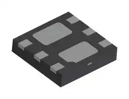
DMN2041UFDB-7
Dual MOSFET, N Channel, 20 V, 20 V, 4.7 A, 4.7 A, 0.04 ohm
⚠️ Reference pricing provided. In case of supply shortages, we will connect you with our trusted procurement partners to ensure your project's continuity.
- Manufacturer: DIODES INC.
- Product type: Dual MOSFETs
- MSL: MSL 1 - Unlimited
- SVHC: No SVHC (25-Jun-2025)
- No. of Pins: 6Pins
- Channel Type: N Channel
- Product Range: -
- Qualification: -
- Transistor Case Style: U-DFN2020
- Operating Temperature Max: 150°C
- Power Dissipation N Channel: 1.4W
- Power Dissipation P Channel: 1.4W
- Drain Source Voltage Vds N Channel: 20V
- Drain Source Voltage Vds P Channel: 20V
- Continuous Drain Current Id N Channel: 4.7A
- Continuous Drain Current Id P Channel: 4.7A
- Drain Source On State Resistance N Channel: 0.04ohm
- Drain Source On State Resistance P Channel: -
| Delivery and price | |
|---|---|
| Units per pack | 1000 |
| Price | 0.318 € |
| Current stock | 1000+ |
| Lead time | 30 days |
Datasheet

**DMN2041UFDB DUAL N-CHANNEL ENHANCEMENT MODE MOSFET**
**==> picture [520 x 562] intentionally omitted <==**
**----- Start of picture text -----**<br>
DMN2041UFDB<br>DUAL N-CHANNEL ENHANCEMENT MODE MOSFET<br>Product Summary Features<br>Device BVDSS RDS(ON) MAX TA = +25°C ID MAX Low On-Resistance Low Input Capacitance<br>40mΩ @ VGS = 4.5V 4.7A Low Profile, 0.6mm Max Height<br>N-Channel 20V<br>65mΩ @ VGS = 2.5V 3.7A ESD Protected Gate<br> Totally Lead-Free & Fully RoHS Compliant (Notes 1 & 2)<br> Halogen and Antimony Free. “Green” Device (Note 3)<br> For automotive applications requiring specific change control<br>Description ption tion<br>(i.e. parts qualified to AEC-Q100/101/200, PPAP capable, and<br>This MOSFET is designed to minimize the on-state resistance manufactured in IATF 16949 certified facilities), please<br>(RDS(ON)) and yet maintain superior switching performance, making it DS(ON)) and yet maintain superior switching performance, making it ) and yet maintain superior switching performance, making it contact us or your local Diodes representative. or your local Diodes representative.<br>ideal for high efficiency power management applications. https://www.diodes.com/quality/product-definitions/-definitions/definitions/<br>Applications Mechanical Data<br> Load Switch Case: U-DFN2020-6<br> Power Management Functions Case Material: Molded Plastic, “Green” Molding Compound;<br> Portable Power Adaptors UL Flammability Classification Rating 94V-0<br> Moisture Sensitivity: Level 1 per J-STD-020<br> Terminals: Finish NiPdAu over Copper Leadframe; Solderable per<br>MIL-STD-202, Method 208 e4<br> Terminal Connections: See Diagram Below<br> Weight: 0.0065 grams (Approximate)<br>U-DFN2020-6 (Type B) D1 D2<br>S2<br>G2<br>D2 G1 G2<br>D1<br>D1<br>D2<br>. &<br>ESD PROTECTED G1 S1 Gate Protection Diode S1 Gate Protection Diode S2<br>Pin1<br>Q1 N-CHANNEL Q2 N-CHANNEL<br>Bottom View<br>Internal Schematic<br>Ordering Information (Note 4)<br>**----- End of picture text -----**<br>
**Totally Lead-Free & Fully RoHS Compliant (Notes 1 & 2)** **Halogen and Antimony Free. “Green” Device (Note 3)** **For automotive applications requiring specific change control Description ption tion (i.e. parts qualified to AEC-Q100/101/200, PPAP capable, and** This MOSFET is designed to minimize the on-state resistance **manufactured in IATF 16949 certified facilities), please** (RDS(ON)) and yet maintain superior switching performance, making it DS(ON)) and yet maintain superior switching performance, making it ) and yet maintain superior switching performance, making it **contact us or your local Diodes representative. or your local Diodes representative.** ideal for high efficiency power management applications. **https://www.diodes.com/quality/product-definitions/-definitions/definitions/**
|**Ordering Informationg Information Information** (Note 4)|**Ordering Informationg Information Information** (Note 4)|**Ordering Informationg Information Information** (Note 4)|
|---|---|---|
||||
|**Part Number**|**Case**|**Packaging**|
|DMN2041UFDB-7|U-DFN2020-6 (TypeB)|3,000/Tape &Reel|
|DMN2041UFDB-13|U-DFN2020-6(Type B)|10,000/Tape & Reel|
Notes: 1. No purposely added lead. Fully EU Directive 2002/95/EC (RoHS), 2011/65/EU (RoHS 2) & 2015/863/EU (RoHS 3) compliant.
2. See https://www.diodes.com/quality/lead-free/ for more information about Diodes Incorporated’s definitions of Halogen- and Antimony-free, "Green" and Lead-free.
3. Halogen- and Antimony-free "Green” products are defined as those which contain <900ppm bromine, <900ppm chlorine (<1500ppm total Br + Cl) and <1000ppm antimony compounds.
4. For packaging details, go to our website at https://www.diodes.com/design/support/packaging/diodes-packaging/.
1 of 8 **www.diodes.com**
DMN2041UFDB Document number: DS37421 Rev. 4 - 2
February 2020 © Diodes Incorporated
**DMN2041UFDB**
## **Marking Information**
Site 1
U-DFN2020-6 (Type B)
D7 = Product Type Marking Code **D7** YM = Date Code Marking Y = Year (ex: H = 2020) M = Month (ex: 9 = September) _ Date Code Key **Year 2014 … 2020 2021 2022 2023 2024 2025 2026 2027 2028 2029** ~~se~~ **Code** B … H I J K L M N O P R **Month Jan Feb Mar Apr May Jun Jul Aug Sep Oct Nov Dec Code** 1 2 3 4 5 6 7 8 9 O N D ~~—— eee~~ ~~**e** e ee eeeeee eeee ee ee ee~~ Site 2 D7 = Product Type Marking Code YWX = Date Code Marking **D7** Y = Year (ex: 0 = 2020) W = Week (ex: a = week 27; z represents week 52 and 53) X = Internal Code (ex: U = Monday) = Date Code Key
**Year 2014 … 2020 2021 2022 2023 2024 2025 2026 2027 2028 2029** ~~ee~~ **Code 4** … **0 1 2** ~~ee~~ **3** ~~ee~~ **4** ~~ee~~ **5** ~~ee~~ **6** ~~ee~~ **7** ~~ee~~ **8 9 Week 1-26 27-52 53 Code** A-Z a-z z ~~eees~~ **Internal Code Sun Mon Tue Wed Thu Fri Sat** ~~ee~~ **Code** T U V W X Y Z
2 of 8 **www.diodes.com**
DMN2041UFDB Document number: DS37421 Rev. 4 - 2
February 2020 © Diodes Incorporated
**DMN2041UFDB**
**Maximum Ratings** (@TA = +25°C, unless otherwise specified.)
|**Maximum Ratingsgss **(@TA = +25°C, unless otherwise specified.)A = +25°C, unless otherwise specified.)= +25°C, unless otherwise specified.)|**Maximum Ratingsgss **(@TA = +25°C, unless otherwise specified.)A = +25°C, unless otherwise specified.)= +25°C, unless otherwise specified.)|**Maximum Ratingsgss **(@TA = +25°C, unless otherwise specified.)A = +25°C, unless otherwise specified.)= +25°C, unless otherwise specified.)|**Maximum Ratingsgss **(@TA = +25°C, unless otherwise specified.)A = +25°C, unless otherwise specified.)= +25°C, unless otherwise specified.)|**Maximum Ratingsgss **(@TA = +25°C, unless otherwise specified.)A = +25°C, unless otherwise specified.)= +25°C, unless otherwise specified.)|**Maximum Ratingsgss **(@TA = +25°C, unless otherwise specified.)A = +25°C, unless otherwise specified.)= +25°C, unless otherwise specified.)|
|---|---|---|---|---|---|
|||||||
|**Characteristic**|||**Symbol**|**Value**|**Unit**|
|Drain-Source Voltage|||VDSS|20|V|
|Gate-Source Voltage|||VGSS|±12|V|
|Continuous Drain Current (Note 5) VGS= 4.5V|Steady<br>State|TA= +25°C<br>TA= +70°C|ID|4.7<br>3.8|A|
||t < 5s|TA= +25°C<br>TA= +70°C|ID|6.1<br>4.9|A|
|Maximum Continuous BodyDiode Forward Current (Note 5)|||IS|2|A|
|Pulsed Drain Current (10µs Pulse, Duty Cycle = 1%)|||IDM|20|A|
## **Thermal Characteristics**
|**Thermal Characteristics**|**Thermal Characteristics**|**Thermal Characteristics**|**Thermal Characteristics**|**Thermal Characteristics**|
|---|---|---|---|---|
||||||
|**Characteristic**||**Symbol**|**Value**|**Unit**|
|Total Power Dissipation (Note 5)|SteadyState|PD|1.4|W|
||t < 5s||2.2||
|Thermal Resistance, Junction to Ambient (Note 5)|SteadyState|RJA|92|°C/W|
||t < 5s||55||
|Thermal Resistance, Junction to Case (Note 5)||RJC|30||
|Operatingand Storage Temperature Range||TJ,TSTG|-55 to +150|°C|
## **Electrical Characteristics** (@TA = +25°C, unless otherwise specified.)
|**Electrical Characteristics**(@TA = +25°C, unless otherwise specified.)A = +25°C, unless otherwise specified.)= +25°C, unless otherwise specified.)|**Electrical Characteristics**(@TA = +25°C, unless otherwise specified.)A = +25°C, unless otherwise specified.)= +25°C, unless otherwise specified.)|**Electrical Characteristics**(@TA = +25°C, unless otherwise specified.)A = +25°C, unless otherwise specified.)= +25°C, unless otherwise specified.)|**Electrical Characteristics**(@TA = +25°C, unless otherwise specified.)A = +25°C, unless otherwise specified.)= +25°C, unless otherwise specified.)|**Electrical Characteristics**(@TA = +25°C, unless otherwise specified.)A = +25°C, unless otherwise specified.)= +25°C, unless otherwise specified.)|**Electrical Characteristics**(@TA = +25°C, unless otherwise specified.)A = +25°C, unless otherwise specified.)= +25°C, unless otherwise specified.)|**Electrical Characteristics**(@TA = +25°C, unless otherwise specified.)A = +25°C, unless otherwise specified.)= +25°C, unless otherwise specified.)|
|---|---|---|---|---|---|---|
||||||||
|**Characteristic**|**Symbol**|**Min**|**Typ **|**Max**<br>~~— ——~~|**Unit**<br>~~——~~|**Test Condition**<br>~~——~~|
|**OFF CHARACTERISTICS(Note 6) **<br>~~— ——~~|||||||
|Drain-Source Breakdown Voltage|BVDSS|20|—|—<br>~~— ——~~|V<br>~~——~~|VGS= 0V, ID= 250μA<br>~~——~~|
|Zero Gate Voltage Drain Current TJ= +25°C<br>~~a~~|IDSS<br>~~a~~|—<br>~~a~~|—<br>~~a~~|1.0<br>~~— ——~~<br>~~a~~|μA<br>~~——~~<br>~~a~~|VDS= 20V, VGS= 0V<br>~~——~~<br>~~a~~|
|Gate-Source Leakage<br>~~a~~|IGSS<br>~~a~~|—<br>~~a~~|—<br>~~a~~|±10<br>~~a~~|μA<br>~~a~~|VGS= ±8V, VDS= 0V<br>~~a~~|
|**ON CHARACTERISTICS(Note 6) **<br>~~IIGDOO~~<br>~~(OO~~|||||||
|Gate Threshold Voltage<br>~~I~~|VGS(TH)<br>~~I~~<br>~~I~~|0.35<br>~~I~~<br>~~I~~<br>~~———————~~|—<br>~~I~~<br>~~GD~~<br>~~———————~~|1.4<br>~~I~~<br>~~OO~~<br>~~———————~~|V<br>~~I~~<br>~~OO~~<br>~~———————~~|VDS= VGS, ID= 250μA<br>~~I~~<br>~~(OO~~<br>~~———————~~|
|Static Drain-Source On-Resistance|RDS(ON)<br>~~I ~~|—<br> ~~I ~~<br>~~———————~~|23<br> ~~GD~~<br>~~———————~~|40<br>~~OO~~<br>~~———————~~|mΩ<br>~~OO~~<br>~~———————~~|VGS= 4.5V, ID= 4.2A<br>~~(OO~~<br>~~———————~~|
|||—<br>~~———————~~|26<br>~~———————~~|65<br>~~———————~~||VGS= 2.5V, ID= 3.3A<br>~~———————~~|
|Diode Forward Voltage<br>~~a~~|VSD<br>~~a~~|—<br>~~———————~~<br>~~a~~|0.75<br>~~———————~~<br>~~a~~|1.2<br>~~———————~~<br>~~a~~|V<br>~~———————~~<br>~~a~~|VGS= 0V, IS= 4.4A<br>~~———————~~<br>~~a~~|
|**DYNAMIC CHARACTERISTICS(Note 7)**<br>~~a~~|||||||
|Input Capacitance<br>~~———~~|Ciss<br>~~———~~|—<br>~~———~~|713<br>~~———~~|—<br>~~———~~|pF<br>~~———~~|VDS= 10V, VGS= 0V,<br>f = 1.0MHz<br>~~———~~|
|Output Capacitance<br>~~———~~<br>~~_——~~|Coss<br>~~———~~|—<br>~~———~~|80<br>~~———~~|—<br>~~———~~|pF<br>~~———~~||
|Reverse Transfer Capacitance<br>~~———~~<br>~~_——~~|Crss<br>~~———~~|—<br>~~———~~|68<br>~~———~~|—<br>~~———~~|pF<br>~~———~~||
|Gate Resistance<br>~~_——~~<br>~~——_—_~~|Rg<br>~~——_—_~~|—|15|—<br>~~ee~~|Ω<br>~~ee~~|VDS= 0V, VGS= 0V, f = 1MHz<br>~~ee~~|
|Total Gate Charge(VGS= 4.5V)<br>~~_——~~<br>~~Pe~~<br>~~——_—_~~|Qg<br>~~——_—_~~|—<br>~~ee~~|8<br>~~ee~~|—<br>~~ee~~<br>~~ee~~|nC<br>~~ee~~|VDS= 10V, ID= 5.5A<br>~~ee~~<br>~~ee~~|
|Total Gate Charge(VGS= 8V)<br>~~_——~~<br>~~Pe~~<br>~~——_—_~~||—<br>~~ee~~|15<br>~~ee~~|—<br>~~ee~~<br>~~ee~~|nC<br>~~ee~~||
|Gate-Source Charge<br>~~_——~~<br>~~Pe~~<br>~~——_—_~~|Qgs<br>~~——_—_~~|—<br>~~ee~~|1.0<br>~~ee~~|—<br>~~ee~~<br>~~ee~~|nC<br>~~ee~~||
|Gate-Drain Charge<br>~~——_—_~~<br>~~————~~|Qgd<br>~~——_—_~~|—|1.1|—<br>~~ee~~<br>~~ee~~|nC<br>~~ee~~<br>~~ee~~||
|Turn-On DelayTime<br>~~——_—_~~<br>~~————~~|tD(ON)<br>~~——_—_~~|—|3.6|—<br>~~ee~~<br>~~ee~~|ns<br>~~ee~~<br>~~ee~~|VDD= 10V, VGS= 4.5V,<br>RL= 2.3Ω, RG= 1Ω<br>~~ee~~<br>~~ee~~|
|Turn-On Rise Time<br>~~——_—_~~<br>~~————~~|tR<br>~~——_—_~~|—|15.9|—<br>~~ee~~<br>~~ee~~|ns<br>~~ee~~<br>~~ee~~||
|Turn-Off DelayTime<br>~~————~~|tD(OFF)|—|16.0|—<br>~~ee~~|ns<br>~~ee~~||
|Turn-Off Fall Time<br>~~————~~|tF|—|2.6|—<br>~~ee~~|ns<br>~~ee~~||
|BodyDiode Reverse RecoveryTime<br>~~————~~<br>~~a~~|tRR<br>~~a~~|—<br>~~a~~|6.6<br>~~a~~|—<br>~~ee~~<br>~~a~~|ns<br>~~ee~~<br>~~a~~|IS= 4.4A, dI/dt = 100A/μs<br>~~ee~~<br>~~a~~|
|Body Diode Reverse Recovery Charge<br>~~a~~|QRR<br>~~a~~|—<br>~~a~~|1.2<br>~~a~~|—<br>~~a~~|nC<br>~~a~~|IS= 4.4A, dI/dt = 100A/μs<br>~~a~~|
Notes: 5. Device mounted on 1” x 1” FR-4 PCB with high coverage 2oz. Copper, single sided. 6. Short duration pulse test used to minimize self-heating effect. 7. Guaranteed by design. Not subject to product testing.
3 of 8 **www.diodes.com**
DMN2041UFDB Document number: DS37421 Rev. 4 - 2
February 2020 © Diodes Incorporated
**DMN2041UFDB**
**==> picture [494 x 672] intentionally omitted <==**
**----- Start of picture text -----**<br>
20 20<br>VGS = 8.0V V = 5.0VDS<br>18 VGS = 4.5V VGS = 1.5V 18<br>16 VGS = 3.0V 16<br>14 14<br>VGS = 2.5V<br>12 Te 12 ee<br>VGS = 2.0V<br>10 {2.--- 10 A<br>86 ,| 86 a7 aa<br>4 4 T = 150°CA T = 85°CA<br>2 | V GS = 1 .0V 2 ff T = 125°CA T = 25°CA<br>T = -55°CA<br>0 p| _T o 0 Za<br>0 0.5 1 1.5 2 2.5 3 0 0.5 1 1.5 2<br>VDS, DRAIN-SOURCE VOLTAGE (V) V , GATE-SOURCE VOLTAGE (V)GS<br>Figure 1 Typical Output Characteristics Figure 2 Typical Transfer Characteristics<br>0.03 0.04<br>0.029 V = 4.5VGS T = 150°CA<br>0.028 0.035 T = 125°CA<br>VGS = 2.5V<br>0.027<br>T = 85°CA<br>0.026 COCR TE 0.03 aGeennneee<br>0.025 VGS = 4.5V<br>0.024 eer ter 0.025 PTT T = 25°CA ITT)<br>CREE a= TTT Le<br>0.023 PCE ee<br>0.022 0.02<br>T = -55°CA<br>0.021<br>0.02 secMza n ezas mum 0.015 PooUOBUREIED<br>0 2 4 6 8 10 12 14 16 18 20 0 2 4 6 8 10 12 14 16 18 20<br>ID, DRAIN-SOURCE CURRENT (A) I , DRAIN CURRENT (A)D<br>Figure 3 Typical On-Resistance vs. Figure 4 Typical On-Resistance vs.<br>Drain Current and Gate Voltage Drain Current and Temperature<br>1.8 0.05<br>VGS 2.5= V<br>1.6 I D = 3.3A<br>VGS 2.5= V<br>0.04 I D = 3.3A<br>1.4<br>Hie VGS = 4.5V (A<br>ID = 4.2A<br>1.2 0.03 V GS 4.5= V<br>cra| LLee ID = 4.2A<br>1<br>tet e 0.02 ra<br>0.8<br>0.6 SRRroe 0.01 PEE<br>-50 -25 0 25 50 75 100 125 150 -50 -25 0 25 50 75 100 125 150<br>TJ, JUNCTION TEMPERATURE (C) TJ, JUNCTION TEMPERATURE (C)<br>Figure 5 On-Resistance Variation with Temperature Figure 6 On-Resistance Variation with Temperature<br>, DRAIN CURRENT (A)<br>ID<br>)<br><br>, DRAIN-SOURCE ON-RESISTANCE (<br>DS(ON)<br>R<br>DS(ON)<br>)<br>, DRAIN-SOURCE ON-RESISTANCE (<br>R<br>DS(ON)<br>, DRAIN-SOURCE<br>R<br>ON-RESISTANCE (NORMALIZED)<br>, DRAIN CURRENT (A)<br>D<br> I<br>)<br>, DRAIN-SOURCE ON-RESISTANCE (<br>R<br>DS(ON)<br>**----- End of picture text -----**<br>
4 of 8
DMN2041UFDB Document number: DS37421 Rev. 4 - 2
February 2020 © Diodes Incorporated
**www.diodes.com**
**DMN2041UFDB**
**==> picture [480 x 674] intentionally omitted <==**
**----- Start of picture text -----**<br>
1 20<br>18<br>0.8 TTTTIT) 16 ee)<br>14<br>0.6 ST[= I = 1mAD TT 12 re ee || | |<br>I = 250µAD 10<br>0.4 TRIwe 8 e e/a |<br>6 T = 150°CA T = 85°CA<br>0.2 LEE EES®SS 4 — T = 125°CA pe) T = 25°CA<br>2<br>T = -55°CA<br>0 SOS 0 7adh ee<br>-50 -25 0 25 50 75 100 125 150 0 0.3 0.6 0.9 1.2 1.5<br>T , JUNCTION TEMPERATURE (C)J V , SOURCE-DRAIN VOLTAGE (V)SD<br>Figure 7 Gate Threshold Variation vs. Junction Temperature Figure 8 Diode Forward Voltage vs. Current<br>10000 8<br>7<br>Se aecaeaea i 6 nEneEPan<br>1000 Ciss VDS = 10V<br>===J ee 54 TTLBane I D 5.5= A ane<br>3<br>100 Coss<br>2<br>Sessa C rss | COT<br>SSSSESE 1 OTr<br>f =1MHz<br>10 to CEE 0 ACCEL<br>0 2 4 6 8 10 12 14 16 18 20 0 2 4 6 8 10 12 14 16<br>VDS, DRAIN-SOURCE VOLTAGE (V) Qg, TOTAL GATE CHARGE (nC)<br>Figure 9 Typical Junction Capacitance Figure 10 Gate Charge<br>100<br>RDS(on)<br>Limited<br>10<br>DC<br>1 P W = 10s<br>PW = 1s<br>P W = 100ms<br>PW = 10ms<br>0.1 Te SIN<br>TJ(max) = 150150癈°C PW = 1ms<br>TA = 2525癈°C<br>VGS = 4.5V P W = 100 祍µs<br>Single Pulse<br>DUT on 1 * MRP Board<br>0.01 all<br>0.1 1 10 100<br>VDS, DRAIN-SOURCE VOLTAGE (V)<br>Figure 11 SOA Safe Operation AreaFigure 12 SOA, Safe Operation Area<br>, SOURCE CURRENT (A)<br>IS<br>, GATE THRESHOLD VOLTAGE (V)<br>GS(TH)<br>V<br>, GATE-SOURCE VOLTAGE (V)<br>GS<br>V<br>, DRAIN CURRENT (A)<br>ID<br>, JUNCTION CAPACITANCE (pF)<br>T<br>C<br> GATE THRESHOLD VOLTAGE (V)<br>GS<br>V<br>**----- End of picture text -----**<br>
5 of 8 **www.diodes.com**
DMN2041UFDB Document number: DS37421 Rev. 4 - 2
February 2020 © Diodes Incorporated
**DMN2041UFDB**
**==> picture [404 x 236] intentionally omitted <==**
**----- Start of picture text -----**<br>
1<br>D = 0.9<br>D = 0.7<br>SSby D = 0.5 oTre<br>D = 0.3 TAI TEE TIemt<br>Po Le<br>ACI<br>0.1<br>D = 0.1 Ee” LIE LIT<br>BSS AM | |<br>eee et te<br>D = 0.05<br>CA 7 All | |<br>NT ae<br>D = 0.02<br>tA HTH ETT CEE ETT<br>0.01 Seee ANI LANE EAT VUELTT<br>EE D = 0.01<br>D = 0.005<br>PA R JA (t) = r(t) * R JA HT<br>AOL R JA = 163163癈°C/W /W tH<br>D = Single Pulse Duty Cycle, D = t1/ t2<br>0.001<br>0.00001 0.0001 0.001 0.01 0.1 1 10 100 1000<br>t1, PULSE DURATION TIME (sec)<br>Figure 13 Transient Thermal ResistanceFigure 12 Transient Thermal Resistance<br>r(t), TRANSIENT THERMAL RESISTANCE<br>**----- End of picture text -----**<br>
6 of 8 **www.diodes.com**
DMN2041UFDB Document number: DS37421 Rev. 4 - 2
February 2020 © Diodes Incorporated
**DMN2041UFDB**
## **Package Outline Dimensions**
Please see http://www.diodes.com/package-outlines.html for the latest version.
## **U-DFN2020-6 (Type B)**
**==> picture [484 x 613] intentionally omitted <==**
**----- Start of picture text -----**<br>
A3<br>A1<br>A<br>Seating Plane U-DFN2020-6<br>Type B<br>D Dim Min Max<br>A 0.545 0.605 0<br>D2 D2 A1 0.00 0.05<br>A3 - -<br>b 0.20 0.30<br>D 1.95 2.075<br>D2 0.50 0.70<br>e - -<br>z1 E 1.95 2.075<br>E2 0.90 1.10<br>E z1 E2<br>k - -<br>k L 0.25 0.35<br>z - - 0<br>z1 - - 0<br>L All Dimensions in mm<br>e<br>z<br>id b<br>Suggested Pad Layout<br>Please see http://www.diodes.com/package-outlines.html for the latest version.<br>U-DFN2020-6 (Type B)<br>X2<br>C<br>Value<br>Dimensions<br>(in mm)<br>C 0.650<br>G 0.150<br>G1 0.450<br>X 0.350<br>X1(2x) X1 0.600<br>X2 1.650<br>Y2 Y1(2x) G Y 0.500<br>G1 Y1 1.000<br>Y2 2.300<br>.<br>Y<br>fi HBev—o X<br>DMN2041UFDB 7 of 8<br>Document number: DS37421 Rev. 4 - 2 www.diodes.com<br>(Pin #1 ID)<br>R0.150<br>**----- End of picture text -----**<br>
|**U-DFN2020-6**<br>**Type Bype Be B**|**U-DFN2020-6**<br>**Type Bype Be B**|**U-DFN2020-6**<br>**Type Bype Be B**|**U-DFN2020-6**<br>**Type Bype Be B**|
|---|---|---|---|
|**Dim**|**Min**|**Maxaxx **|**Typ**|
|**A**|0.545.545545455|0.605.605605|0.575|
|**A1**|0.00.0000|0.05.0505|0.02|
|**A3**|-|-|0.13|
|**b**|0.20.200|0.30.3030|0.25|
|**D**|1.9595|2.075075755|2.00|
|**D2**|0.50.5050|0.70.700|0.60|
|**e**|-|-|0.65|
|**E**|1.9595|2.075075755|2.00|
|**E2**|0.90.9090|1.100|1.00|
|**k**|-|-|0.45|
|**L**|0.25.255|0.35.3535|0.30|
|**z**|-|-|0.225|
|**z1**|-|-|0.175|
|**All Dimensions in mm**||||
February 2020 © Diodes Incorporated
**DMN2041UFDB**
## **IMPORTANT NOTICE**
DIODES INCORPORATED MAKES NO WARRANTY OF ANY KIND, EXPRESS OR IMPLIED, WITH REGARDS TO THIS DOCUMENT, INCLUDING, BUT NOT LIMITED TO, THE IMPLIED WARRANTIES OF MERCHANTABILITY AND FITNESS FOR A PARTICULAR PURPOSE (AND THEIR EQUIVALENTS UNDER THE LAWS OF ANY JURISDICTION).
Diodes Incorporated and its subsidiaries reserve the right to make modifications, enhancements, improvements, corrections or other changes without further notice to this document and any product described herein. Diodes Incorporated does not assume any liability arising out of the application or use of this document or any product described herein; neither does Diodes Incorporated convey any license under its patent or trademark rights, nor the rights of others. Any Customer or user of this document or products described herein in such applications shall assume all risks of such use and will agree to hold Diodes Incorporated and all the companies whose products are represented on Diodes Incorporated website, harmless against all damages.
Diodes Incorporated does not warrant or accept any liability whatsoever in respect of any products purchased through unauthorized sales channel. Should Customers purchase or use Diodes Incorporated products for any unintended or unauthorized application, Customers shall indemnify and hold Diodes Incorporated and its representatives harmless against all claims, damages, expenses, and attorney fees arising out of, directly or indirectly, any claim of personal injury or death associated with such unintended or unauthorized application.
Products described herein may be covered by one or more United States, international or foreign patents pending. Product names and markings noted herein may also be covered by one or more United States, international or foreign trademarks.
This document is written in English but may be translated into multiple languages for reference. Only the English version of this document is the final and determinative format released by Diodes Incorporated.
## **LIFE SUPPORT**
Diodes Incorporated products are specifically not authorized for use as critical components in life support devices or systems without the express written approval of the Chief Executive Officer of Diodes Incorporated. As used herein:
- A. Life support devices or systems are devices or systems which:
1. are intended to implant into the body, or
2. support or sustain life and whose failure to perform when properly used in accordance with instructions for use provided in the labeling can be reasonably expected to result in significant injury to the user.
B. A critical component is any component in a life support device or system whose failure to perform can be reasonably expected to cause the failure of the life support device or to affect its safety or effectiveness.
Customers represent that they have all necessary expertise in the safety and regulatory ramifications of their life support devices or systems, and acknowledge and agree that they are solely responsible for all legal, regulatory and safety-related requirements concerning their products and any use of Diodes Incorporated products in such safety-critical, life support devices or systems, notwithstanding any devices- or systems-related information or support that may be provided by Diodes Incorporated. Further, Customers must fully indemnify Diodes Incorporated and its representatives against any damages arising out of the use of Diodes Incorporated products in such safety-critical, life support devices or systems.
Copyright © 2020, Diodes Incorporated
**www.diodes.com**
8 of 8 **www.diodes.com**
DMN2041UFDB Document number: DS37421 Rev. 4 - 2
February 2020 © Diodes Incorporated
Updated at June 9, 2026
About Novapart
Novapart is a B2B electronic component broker specialising in stock shortages and cost reduction. We source hard-to-find parts and identify compliant alternatives across a catalogue of 410,000+ components from 500+ manufacturers.
Learn more →Stock Shortage Specialist
When a component is unavailable, discontinued or has an unacceptable lead time, we tap into our network of vetted European and Asian distributors to source what you need — without compromising on quality or traceability.
Request a quote →Compliant Alternatives
We identify pin-to-pin, electrically equivalent substitutes that meet the same certifications (RoHS, AEC-Q100, REACH) as your original specification — validated against datasheets, not just part numbers. Often at a lower cost.
BOM Analysis service →