
Image not available
Illustrative purposes only

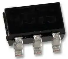
DMMT2907A-7
Bipolar Transistor Array, Dual PNP, 60 V, 600 mA
⚠️ Reference pricing provided. In case of supply shortages, we will connect you with our trusted procurement partners to ensure your project's continuity.
- Manufacturer: DIODES INC.
- Product type: Bipolar Junction Transistor Arrays - BJT
- MSL: MSL 1 - Unlimited
- SVHC: No SVHC (25-Jun-2025)
- No. of Pins: 6Pins
- Product Range: -
- Qualification: AEC-Q101
- Transistor Mounting: Surface Mount
- Transistor Polarity: Dual PNP
- Power Dissipation NPN: -
- Power Dissipation PNP: 900mW
- Transistor Case Style: SOT-26
- Transition Frequency NPN: -
- Transition Frequency PNP: 307MHz
- Operating Temperature Max: 150°C
- DC Current Gain hFE Min NPN: -
- DC Current Gain hFE Min PNP: 50hFE
- Continuous Collector Current NPN: -
- Continuous Collector Current PNP: 600mA
- Collector Emitter Voltage Max NPN: -
- Collector Emitter Voltage Max PNP: 60V
| Delivery and price | |
|---|---|
| Units per pack | 5000 |
| Price | 0.114 € |
| Current stock | 10+ |
| Lead time | 30 days |
Datasheet

**Green** ~~&~~
**DMMT2907A** 7
**Green 60V DUAL PNP SMALL SIGNAL TRANSISTOR IN SOT26**
## **Features**
## **Mechanical Data**
- BVCEO > -60V
- ICM = -1A Peak Pulse Current
- General Purpose PNP Transistors Ideally Suited for Low Power Amplification and Switching Applications
- Dual Transistors in a Single SOT26 Package, Taking Half of the Footprint of Two Equivalent Transistors in SOT23
- Epitaxial Planar Die Construction
- Case: SOT26
- Case Material: Molded Plastic, “Green” Molding Compound. UL Flammability Classification Rating 94V-0
- Moisture Sensitivity: Level 1 per J-STD-020
- Terminals: Finish – Matte Tin Plated Leads, Solderable per MILSTD-202, Method 208
- Weight: 0.015 grams (Approximate)
- **Totally Lead-Free & Fully RoHS Compliant (Notes 1 & 2)**
- **Halogen and Antimony Free. “Green” Device (Note 3)**
- **Qualified to AEC-Q101 Standards for High Reliability**
**==> picture [436 x 123] intentionally omitted <==**
**----- Start of picture text -----**<br>
SOT26 C1 C2<br>B1 C1<br>' || |<br>B1 B2 E2 E1<br>B2 i: C2<br>| | |<br>E1 E2<br>Top View Device Symbol Top View<br>Pin-Out<br>**----- End of picture text -----**<br>
## **Ordering Information** (Note 4)
|**Ordering Informationg Information Information** (Note 4)|**Ordering Informationg Information Information** (Note 4)|**Ordering Informationg Information Information** (Note 4)|**Ordering Informationg Information Information** (Note 4)|**Ordering Informationg Information Information** (Note 4)|**Ordering Informationg Information Information** (Note 4)|
|---|---|---|---|---|---|
|**Product**<br>**Compliance**<br>**Marking**<br>**Reel Size(inches)**<br>**Tape Width(mm)**<br>**Quantity per Reel**<br>DMMT2907A-7<br>AEC-Q101<br>907<br>7<br>8<br>3,000||||||
|**Product**|**Compliance**|**Marking**|**Reel Size(inches)**|**Tape Width(mm)**|**Quantity per Reel**|
|DMMT2907A-7|AEC-Q101|907|7|8|3,000|
- Notes: 1. No purposely added lead. Fully EU Directive 2002/95/EC (RoHS) & 2011/65/EU (RoHS 2) compliant.
2. See http://www.diodes.com/quality/lead_free.html for more information about Diodes Incorporated’s definitions of Halogen- and Antimony-free, "Green" and Lead-free.
3. Halogen- and Antimony-free "Green” products are defined as those which contain <900ppm bromine, <900ppm chlorine (<1500ppm total Br + Cl) and <1000ppm antimony compounds.
4. For packaging details, go to our website at http://www.diodes.com/products/packages.html.
## **Marking Information**
**==> picture [214 x 70] intentionally omitted <==**
**----- Start of picture text -----**<br>
SOT26<br>907 = Product Type Marking Code<br>YM = Date Code Marking<br>907 Y or Y = Year (ex: C = 2015)<br>M or M = Month (ex: 9 = September)<br>YM<br>**----- End of picture text -----**<br>
**==> picture [525 x 61] intentionally omitted <==**
**----- Start of picture text -----**<br>
Date Code Key<br>Year 2015 2016 2017 2018 2019 2020 2021 2022 2023 2024 2025<br>-fF Code C D E F G H I — —f J K —f L — M —~<br>Month Jan Feb Mar Apr May Jun Jul Aug Sep Oct Nov Dec<br>+ Code 1 2 3 4 5 6 7 8 9 O N — D<br>**----- End of picture text -----**<br>
1 of 7 **www.diodes.com**
DMMT2907A Document Number: DS35106 Rev: 2 - 2
November 2015 © Diodes Incorporated
**DMMT2907A**
**Absolute Maximum Ratings** (@TA = +25°C, unless otherwise specified.)
**==> picture [488 x 64] intentionally omitted <==**
**----- Start of picture text -----**<br>
|||||
|---|---|---|---|
|Characteristic|Symbol|Value|Unit|
|Collector-Base Voltage|VCBO|-60|V|
|Collector-Emitter Voltage|VCEO|-60|V|
|Emitter-Base Voltage|VEBO|-5|V|
|Continuous Collector Current|IC|-600|mA|
|Peak Pulsed Collector Current|ICM|-1|A|
**----- End of picture text -----**<br>
## **Thermal Characteristics** (@TA = +25°C, unless otherwise specified.)
**==> picture [493 x 89] intentionally omitted <==**
**----- Start of picture text -----**<br>
||||||
|---|---|---|---|---|
|Characteristic|Symbol|Value|Unit|
|1.28|
|(Notes 6 & 7)|
|Power Dissipation|10.3|W|
|Linear Derating Factor|PD|0.90|mW/°C|
|(Notes 5 & 7)|7.14|
|(Notes 6 & 7)|97|
|Thermal Resistance, Junction to Ambient|(Notes 5 & 7)|RθJA|140|°C/W|
|Thermal Resistance, Junction to Lead|(Note 8)|RθJL|113|
|Operating and Storage Temperature Range|TJ, TSTG|-55 to +150|°C|
**----- End of picture text -----**<br>
## **ESD Ratings** (Note 9)
**==> picture [516 x 32] intentionally omitted <==**
**----- Start of picture text -----**<br>
||||||
|---|---|---|---|---|
|Characteristic|Symbol|Value|Unit|JEDEC Class|
|Electrostatic Discharge – Human Body Model|ESD HBM|4,000|V|3A|
|Electrostatic Discharge – Machine Model|ESD MM|400|V|C|
**----- End of picture text -----**<br>
Notes: 5. For a device surface mounted on 25mm x 25mm x 1.6mm FR4 PCB with high coverage of single sided 1oz copper, in still air conditions; the device is measured when operating in a steady-state condition.
6. Same as Note 5, except the device is measured at t 5 seconds.
7. For a dual device with one active die.
8. Thermal resistance from junction to solder-point (at the end of the collector lead).
9. Refer to JEDEC specification JESD22-A114 and JESD22-A115.
2 of 7 **www.diodes.com**
DMMT2907A Document Number: DS35106 Rev: 2 - 2
November 2015 © Diodes Incorporated
**DMMT2907A** [|
## LIODES.
## **Thermal Characteristics and Derating Information**
**==> picture [444 x 354] intentionally omitted <==**
**----- Start of picture text -----**<br>
1.0<br>25mm x 25mm<br>1 V 1oz Cu<br>CE(sat) ET 0.8 HAT | |]<br>POATAT Limited fOTTOTNSNINNKEN ENTENK ilil 0.6 PP WN NOGNN |) 4 4<br>DC 1s<br>100m Yo EORAN 0.4 NK<br>100ms<br>a 25mm x 25mm 1oz Cu eee 10ms 1ms Ph ’ NINN INONUINT 0.2 ‘N\<br>10m | T Single Pulseamb =25°C | 100µs 0.0 COINS\<br>100m 1 10 100 0 20 40 60 80 100 120 140 160<br>-VCE Collector-Emitter Voltage (V) Temperature (°C)<br>Safe Operating Area Derating Curve<br>140 25mm x 25mm 1oz Cu 25mm x 25mm 1oz Cu<br>120 ai Tamb=25°C ania ci 100 EI 0 A T amb =25°C |<br>Single Pulse<br>100 SAA oA Hee alll | Il SSSFEAHERECTeri i<br>D=0.5<br>80<br>10<br>60 La LaiFae TTT L/SBaisSeth ES<br>40 D=0.2 TT ha Single Pulse il SEH H HaSHH<br>D=0.05<br>20 Ye il 1 CAT TTS aH<br>D=0.1<br>0 eee MD Ui ll UN SSEr Sgt asset meri amerty Smet mast<br>100µ 1m 10m 100m 1 10 100 1k 100µ 1m 10m 100m 1 10 100 1k<br>Pulse Width (s) Pulse Width (s)<br>Transient Thermal Impedance Pulse Power Dissipation<br> Collector Current (A)<br>C<br>-I<br> Max Power Dissipation (W)<br> Maximum Power (W)<br>Thermal Resistance (°C/W)<br>**----- End of picture text -----**<br>
3 of 7 **www.diodes.com**
DMMT2907A Document Number: DS35106 Rev: 2 - 2
November 2015 © Diodes Incorporated
**DMMT2907A**
**Electrical Characteristics** (@TA = +25°C unless otherwise specified.)
|**Electrical Characteristics** (@TA = +25°C unless otherwise specified.)A = +25°C unless otherwise specified.)= +25°C unless otherwise specified.)|**Electrical Characteristics** (@TA = +25°C unless otherwise specified.)A = +25°C unless otherwise specified.)= +25°C unless otherwise specified.)|**Electrical Characteristics** (@TA = +25°C unless otherwise specified.)A = +25°C unless otherwise specified.)= +25°C unless otherwise specified.)|**Electrical Characteristics** (@TA = +25°C unless otherwise specified.)A = +25°C unless otherwise specified.)= +25°C unless otherwise specified.)|**Electrical Characteristics** (@TA = +25°C unless otherwise specified.)A = +25°C unless otherwise specified.)= +25°C unless otherwise specified.)|**Electrical Characteristics** (@TA = +25°C unless otherwise specified.)A = +25°C unless otherwise specified.)= +25°C unless otherwise specified.)|**Electrical Characteristics** (@TA = +25°C unless otherwise specified.)A = +25°C unless otherwise specified.)= +25°C unless otherwise specified.)|
|---|---|---|---|---|---|---|
||||||||
|**Characteristic**<br>~~ee~~|**Symbol**<br>~~ee~~|**Min**<br>~~ee~~|**Typ**<br>~~ee~~|**Max**<br>~~ee~~|**Unit**<br>~~ee~~|**Test Condition**<br>~~ee~~|
|**OFF CHARACTERISTICS**<br>~~ee~~|||||||
|Collector-Base Breakdown Voltage<br>~~ee~~|BVCBO<br>~~ee~~|-60<br>~~ee~~|<br>~~ee~~|<br>~~ee~~|V<br>~~ee~~|IC= -10µA,IE= 0<br>~~ee~~|
|Collector-Emitter Breakdown Voltage(Note 10)<br>~~ee~~|BVCEO<br>~~ee~~|-60<br>~~ee~~|<br>~~ee~~|<br>~~ee~~|V<br>~~ee~~|IC= -10mA,IB= 0<br>~~ee~~|
|Emitter-Base Breakdown Voltage<br>~~ee~~|BVEBO<br>~~ee~~|-5<br>~~ee~~|<br>~~ee~~|<br>~~ee~~|V<br>~~ee~~|IE= -10µA,IC= 0<br>~~ee~~|
|Collector-Base Cut-Off Current<br>~~I~~|ICBO<br>~~I~~|<br>~~I~~|<br>~~I~~|-10<br>~~I~~|nA<br>~~I~~|VCB= -50V,IE= 0<br>~~I~~|
|||<br>~~I~~|<br>~~I~~|-10<br>~~I~~|µA<br>~~I~~|VCB= -50V,IE= 0,TA= +150°C<br>~~I~~|
|Collector-Emitter Cut-Off Current<br>~~I~~|ICEV<br>~~I~~|<br>~~I~~|<br>~~I~~|±50<br>~~I~~|nA<br>~~I~~|VCE= -30V,VBE= ±0.25V<br>~~I~~|
|Base-Emitter Cut-Off Current<br>~~ff~~|IBEV<br>~~ff~~|<br>~~ff~~|<br>~~ff~~|±50<br>~~ff~~|nA<br>~~ff~~|VCE= -30V,VBE= ±0.25V<br>~~ff~~|
|**ON CHARACTERISTICS**(Note 10)<br>~~eeee~~<br>~~PO~~|||||||
|DC Current Gain<br>~~===~~|hFE<br>~~===~~|75<br>~~ee~~<br>~~ee~~<br>~~===~~|<br>~~ee~~<br>~~ee~~<br>~~===~~|<br>~~===~~|<br>~~===~~<br>~~———————~~|IC= -100A,VCE= -10V<br>~~PO~~<br>~~PO~~<br>~~===~~|
|||100<br>~~ee ~~<br>~~ee~~<br>~~===~~|<br> ~~ee~~<br>~~ee~~<br>~~===~~|<br>~~===~~||IC= -1.0mA,VCE= -10V<br>~~PO~~<br>~~PO~~<br>~~===~~|
|||100<br>~~ee ~~<br>~~===~~|<br> ~~ee~~<br>~~===~~|<br>~~===~~||IC= -10mA,VCE= -10V<br>~~PO~~<br>~~===~~|
|||100<br>~~===~~|<br>~~===~~<br>~~———————~~|300<br>~~===~~<br>~~———————~~||IC= -150mA,VCE= -10V<br>~~===~~<br>~~———————~~|
|||50<br>~~===~~|<br>~~===~~<br>~~———————~~|<br>~~===~~<br>~~———————~~||IC= -500mA,VCE= -10V<br>~~===~~<br>~~———————~~|
|Collector-Emitter Saturation Voltage|VCE(sat)||<br>~~———————~~|-0.4<br>~~———————~~|V<br>~~———————~~<br>~~——————————~~|IC= -150mA,IB= -15mA<br>~~———————~~<br>~~——————————~~|
||||<br>~~———————~~|-1.6<br>~~———————~~||IC= -500mA,IB= -50mA<br>~~———————~~<br>~~——————————~~|
|Base-Emitter Saturation Voltage|VBE(sat)||<br>~~———————~~|-1.3<br>~~———————~~|V<br>~~———————~~<br>~~——————————~~|IC= -150mA,IB= -15mA<br>~~———————~~<br>~~——————————~~|
|||||-2.6||IC= -500mA,IB= -50mA<br>~~——————————~~|
|**SMALL SIGNAL CHARACTERISTICS**<br>~~——————————~~<br>~~II GOOO~~|||||||
|Output Capacitance<br>~~I~~|Cobo<br>~~I~~<br>~~I~~|<br>~~I~~<br>~~I GO~~|5.2<br>~~I~~<br>~~GO~~|<br>~~I~~<br>~~GO~~|pF<br>~~I~~<br>~~OO~~|VCB= -10V,f = 1.0MHz,IE= 0mA<br>~~I~~<br>~~OO~~|
|Input Capacitance<br>~~ee~~|Cibo<br>~~I ~~<br>~~ee~~|<br> ~~I GO~~<br>~~ee~~|16.3<br>~~GO~~<br>~~ee~~|<br>~~GO ~~<br>~~ee~~|pF<br> ~~OO~~<br>~~ee~~|VEB= -2.0V,f = 1.0MHz,IC= 0mA<br>~~OO~~<br>~~ee~~|
|Current Gain-Bandwidth Product<br>~~ee~~|fT<br>~~ee~~<br>~~ee~~|200<br>~~ee~~<br>~~ee~~|307<br>~~ee~~<br>~~ee~~|<br>~~ee~~<br>~~ee~~|MHz<br>~~ee~~|VCE= -2V,IC= -10mA,f = 100MHz<br>~~ee~~|
|Turn-On Time<br>~~I~~<br>~~e~~|ton<br>~~I~~<br>~~e~~<br>~~ee~~|<br>~~I~~<br>~~e~~~~**e**~~<br>~~ee~~|<br>~~I~~<br>~~**e**~~<br>~~ee~~|21<br>~~I~~<br>~~**e**~~<br>~~ee~~|ns<br>~~I~~<br>~~**e**~~|VCC= -30V IC= -150mA,<br>IB1= -15mA<br>~~**e**~~|
|DelayTime<br>~~e~~|td<br>~~e~~<br>~~ee~~|<br>~~e~~~~**e**~~<br>~~ee~~|<br>~~**e**~~<br>~~ee~~|5.5<br>~~**e**~~<br>~~ee~~|ns<br>~~**e**~~||
|Rise Time<br>~~e~~|tr<br>~~e~~<br>~~ee~~|<br>~~e~~~~**e**~~<br>~~ee~~|<br>~~**e**~~<br>~~ee~~|15.3<br>~~**e**~~<br>~~ee~~|ns<br>~~**e**~~||
|Turn-Off Time<br>~~e~~<br>~~ee~~|toff<br>~~e~~<br>~~ee~~<br>~~ee~~|<br>~~e~~~~**e**~~<br>~~ee~~<br>~~ee~~|<br>~~**e**~~<br>~~ee~~<br>~~ee~~|200<br>~~**e**~~<br>~~ee~~<br>~~ee~~|ns<br>~~**e**~~<br>~~ee~~|VCC= -6V<br>IC= -150mA, IB1= IB2= -15mA<br>~~**e**~~<br>~~ee~~|
|Storage Time<br>~~ee~~|ts<br>~~ee~~<br>~~ee~~|<br>~~ee ~~<br>~~ee~~|<br> ~~ee~~<br>~~ee~~|160<br>~~ee~~<br>~~ee~~|ns<br>~~ee~~||
|Fall Time<br>~~ee~~|tf<br>~~ee~~|<br>~~ee~~|<br>~~ee~~|40<br>~~ee~~|ns<br>~~ee~~||
4 of 7 **www.diodes.com**
DMMT2907A Document Number: DS35106 Rev: 2 - 2
November 2015 © Diodes Incorporated
**DMMT2907A**
## **Typical Electrical Characteristics** (@TA = +25°C, unless otherwise specified.)
**==> picture [448 x 549] intentionally omitted <==**
**----- Start of picture text -----**<br>
1.0<br>V =5V<br>125°C CE 0.9 I C /I B =10<br>250 HHH HH pF} 444} +]<br>Temata 0.8 =<br>200 EH 25°C eeertms Nl 0.70.6 Seiapoee ee 125 oe °C ee/<br>25°C<br>150 0.5<br>-40°C 0.4<br>100 NTT — a, ae<br>0.3<br>0.2<br>50<br>0.1 -40°C<br>nO RTT —ee<br>0 ee ell 0.0 a<br>1m 10m 100m 1 10m 100m<br>- IC Collector Current (A) - IC Collector Current (A)<br>h v I V v I<br>FE C CE(sat) C<br>1.2<br>1.2 I C /I B =10 Th Coa V CE =5V T_T<br>THEE 1.0 Oe 9 ll<br>1.0 PT AT CI ei<br>-40°C<br>A -40°C AN 0.8 HT TT<br>0.8 Pe 25°C TTI a 25°C elle<br>Tare =<br>0.6 TT ee I 0.6 eerA<br>125°C 125°C<br>ee tt<br>0.4 eri CO on 0.4 cllettTI ii<br>1m 10m 100m 1 1m 10m 100m 1<br>- IC Collector Current (A) - IC Collector Current (A)<br>V v I<br>V v I BE(on) C<br>BE(sat) C<br>10 30<br>V = 35V<br>CB f = 1MHz<br>po TT<br>1 |es eeaes es > 20 TE-PPSeee. LUT Til<br>|_| | rt a.<br>SSS SSS CML Cibo Ll<br>0.1 a oe 10<br>SSSATE SS aa Cobo<br>0.01 Feot | {| { | { tT[ 4 0 TIECET ATT Til il<br>25 50 75 100 125 10m 100m 1 10 100<br> TA Ambient Temperature (°C) - Voltage(V)<br>I v T Capacitance v Voltage<br>CBO A<br>Typical Gain (hFE)<br> (V)<br>CE(sat)<br>- V<br> (V) (V)<br>BE(sat) BE(on)<br>- V - V<br> Collector Current (nA)<br>CBO Capacitance (pF)<br>- I<br>**----- End of picture text -----**<br>
5 of 7 **www.diodes.com**
DMMT2907A Document Number: DS35106 Rev: 2 - 2
November 2015 © Diodes Incorporated
**DMMT2907A**
## **Package Outline Dimensions**
Please see AP02002 at http://www.diodes.com/datasheets/ap02002.pdf for the latest version.
## **SOT26**
**==> picture [458 x 209] intentionally omitted <==**
**----- Start of picture text -----**<br>
D<br>SOT26<br>Dim Min Max Typ<br>A1 0.013 0.10 0.05<br>E1 : ou Lo E | a=== A2 1.00 1.30 1.10<br>A3 0.70 0.80 0.75<br>b 0.35 0.50 0.38<br>c 0.10 0.20 0.15<br>D 2.90 3.10 3.00<br>Coal e – – 0.95<br>b e1 – – 1.90<br>a1 E 2.70 3.00 2.80<br>e1 E1 1.50 1.70 1.60<br>L 0.35 0.55 0.40<br>a – – 8°<br>a1 – – 7°<br>A2<br>A1 All Dimensions in mm<br>A3<br>Seating Plane a<br>L<br>e c<br>**----- End of picture text -----**<br>
## **Suggested Pad Layout**
Please see AP02001 at http://www.diodes.com/datasheets/ap02001.pdf for the latest version.
**SOT26**
**==> picture [140 x 134] intentionally omitted <==**
**----- Start of picture text -----**<br>
_ C1 _<br>Y1 O00 G C<br>a |<br>Y<br>“oe X<br>**----- End of picture text -----**<br>
|**Dimensions Value**|**Dimensions Value(in mm)**|
|---|---|
|**C**|**()**<br>2.40|
|**C1**|0.95|
|**G**|1.60|
|**X**|0.55|
|**Y**|0.80|
|**Y1**|3.20|
6 of 7 **www.diodes.com**
DMMT2907A Document Number: DS35106 Rev: 2 - 2
November 2015 © Diodes Incorporated
**DMMT2907A**
## **IMPORTANT NOTICE**
DIODES INCORPORATED MAKES NO WARRANTY OF ANY KIND, EXPRESS OR IMPLIED, WITH REGARDS TO THIS DOCUMENT, INCLUDING, BUT NOT LIMITED TO, THE IMPLIED WARRANTIES OF MERCHANTABILITY AND FITNESS FOR A PARTICULAR PURPOSE (AND THEIR EQUIVALENTS UNDER THE LAWS OF ANY JURISDICTION).
Diodes Incorporated and its subsidiaries reserve the right to make modifications, enhancements, improvements, corrections or other changes without further notice to this document and any product described herein. Diodes Incorporated does not assume any liability arising out of the application or use of this document or any product described herein; neither does Diodes Incorporated convey any license under its patent or trademark rights, nor the rights of others. Any Customer or user of this document or products described herein in such applications shall assume all risks of such use and will agree to hold Diodes Incorporated and all the companies whose products are represented on Diodes Incorporated website, harmless against all damages.
Diodes Incorporated does not warrant or accept any liability whatsoever in respect of any products purchased through unauthorized sales channel. Should Customers purchase or use Diodes Incorporated products for any unintended or unauthorized application, Customers shall indemnify and hold Diodes Incorporated and its representatives harmless against all claims, damages, expenses, and attorney fees arising out of, directly or indirectly, any claim of personal injury or death associated with such unintended or unauthorized application.
Products described herein may be covered by one or more United States, international or foreign patents pending. Product names and markings noted herein may also be covered by one or more United States, international or foreign trademarks.
This document is written in English but may be translated into multiple languages for reference. Only the English version of this document is the final and determinative format released by Diodes Incorporated.
## **LIFE SUPPORT**
Diodes Incorporated products are specifically not authorized for use as critical components in life support devices or systems without the express written approval of the Chief Executive Officer of Diodes Incorporated. As used herein:
- A. Life support devices or systems are devices or systems which:
1. are intended to implant into the body, or
2. support or sustain life and whose failure to perform when properly used in accordance with instructions for use provided in the labeling can be reasonably expected to result in significant injury to the user.
B. A critical component is any component in a life support device or system whose failure to perform can be reasonably expected to cause the failure of the life support device or to affect its safety or effectiveness.
Customers represent that they have all necessary expertise in the safety and regulatory ramifications of their life support devices or systems, and acknowledge and agree that they are solely responsible for all legal, regulatory and safety-related requirements concerning their products and any use of Diodes Incorporated products in such safety-critical, life support devices or systems, notwithstanding any devices- or systems-related information or support that may be provided by Diodes Incorporated. Further, Customers must fully indemnify Diodes Incorporated and its representatives against any damages arising out of the use of Diodes Incorporated products in such safety-critical, life support devices or systems.
Copyright © 2015, Diodes Incorporated
**www.diodes.com**
7 of 7 **www.diodes.com**
DMMT2907A Document Number: DS35106 Rev: 2 - 2
November 2015 © Diodes Incorporated
Updated at March 26, 2026
About Novapart
Novapart is a B2B electronic component broker specialising in stock shortages and cost reduction. We source hard-to-find parts and identify compliant alternatives across a catalogue of 410,000+ components from 500+ manufacturers.
Learn more →Stock Shortage Specialist
When a component is unavailable, discontinued or has an unacceptable lead time, we tap into our network of vetted European and Asian distributors to source what you need — without compromising on quality or traceability.
Request a quote →Compliant Alternatives
We identify pin-to-pin, electrically equivalent substitutes that meet the same certifications (RoHS, AEC-Q100, REACH) as your original specification — validated against datasheets, not just part numbers. Often at a lower cost.
BOM Analysis service →