
Image not available
Illustrative purposes only

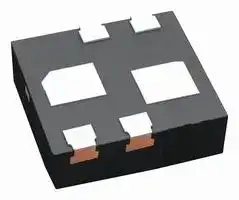
DMC2004LPK-7
Dual MOSFET, Complementary N and P Channel, 20 V, 20 V, 750 mA, 750 mA, 0.55 ohm
⚠️ Reference pricing provided. In case of supply shortages, we will connect you with our trusted procurement partners to ensure your project's continuity.
- Manufacturer: DIODES INC.
- Product type: Dual MOSFETs
- MSL: MSL 1 - Unlimited
- SVHC: No SVHC (25-Jun-2025)
- No. of Pins: 6Pins
- Channel Type: Complementary N and P Channel
- Product Range: -
- Qualification: -
- Transistor Case Style: X1-DFN1612
- Operating Temperature Max: 150°C
- Power Dissipation N Channel: 500mW
- Power Dissipation P Channel: 500mW
- Drain Source Voltage Vds N Channel: 20V
- Drain Source Voltage Vds P Channel: 20V
- Continuous Drain Current Id N Channel: 750mA
- Continuous Drain Current Id P Channel: 750mA
- Drain Source On State Resistance N Channel: 0.55ohm
- Drain Source On State Resistance P Channel: 0.9ohm
| Delivery and price | |
|---|---|
| Units per pack | 1000 |
| Price | 0.142 € |
| Current stock | 1000+ |
| Lead time | 30 days |
Datasheet

~~x~~ **Green** **DMC2004LPK** ## **COMPLEMENTARY PAIR ENHANCEMENT MODE FIELD EFFECT TRANSISTOR** ## **Features** - Low On-Resistance - Low Gate Threshold Voltage VGS(th) < 1V - Low Input Capacitance - Fast Switching Speed - Low Input/Output Leakage - Complementary Pair MOSFET - Ultra-Small Surface Mount Package - ESD Protected Gate ## **Mechanical Data** - Case: X1-DFN1612-6 - Case Material: Molded Plastic, “Green” Molding - Compound. UL Flammability Classification Rating 94V-0 - Moisture Sensitivity: Level 1 per J-STD-020C - Terminal Connections: See Diagram - Terminals: Finish – NiPdAu over Copper leadframe. Solderable per MIL-STD-202, Method 208 **e4** - Weight: 0.003 grams (approximate) - **Lead-Free Finish; RoHS Compliant (Notes 1 & 2)** - **Halogen and Antimony Free. “Green” Device (Note 3)** - **For automotive applications requiring specific change control (i.e.: parts qualified to AEC-Q100/101/200, PPAP capable, and manufactured in IATF 16949 certified facilities), please refer to the related automotive grade (Qsuffix) part. A listing can be found at -** - **https://www.diodes.com/products/automotive/automotive products/.** - **This part is qualified to JEDEC standards (as references in AEC-Q) for High Reliability. https://www.diodes.com/quality/product-definitions/** X1-DFN1612-6 **==> picture [230 x 92] intentionally omitted <==** **----- Start of picture text -----**<br> D1 G2 S2<br>6 5 4<br>Q1 Q2<br>(a<br>ESD protected<br>1 2 3<br>S1 G1 D2<br>TOP VIEW<br>Internal Schematic<br>**----- End of picture text -----**<br> ## **Ordering Information** (Note 4) |**Part Number**|**Case**|**Packaging**| |---|---|---| |DMC2004LPK-7|X1-DFN1612-6|3000/Tape &Reel| Notes: 1. EU Directive 2002/95/EC (RoHS), 2011/65/EU (RoHS 2) & 2015/863/EU (RoHS 3) compliant. All applicable RoHS exemptions applied. 2. See https://www.diodes.com/quality/lead-free/ for more information about Diodes Incorporated’s definitions of Halogen- and Antimony-free, "Green" and Lead-free. 3. Halogen- and Antimony-free "Green” products are defined as those which contain <900ppm bromine, <900ppm chlorine (<1500ppm total Br + Cl) and <1000ppm antimony compounds. 4. For packaging details, go to our website at https://www.diodes.com/design/support/packaging/diodes-packaging/. ## **Marking Information** C1 = Marking Code YM = Date Code Marking C1 Y = Year (ex: Z = 2012) M = Month (ex: 9 = September) |Date CodeKey<br>**Year**<br>**Code**<br>~~**a**~~|**2012**<br>Z|**2012**<br>Z|||**2013**<br>A|||**2014**<br>**2015**<br>B<br>C|**2014**<br>**2015**<br>B<br>C|||**2016**<br>D|||**2017**<br>E|**2018**<br>F| |---|---|---|---|---|---|---|---|---|---|---|---|---|---|---|---|---| |**Month**<br>**Code**<br>~~rs~~|**Jan**<br>1<br>~~ee~~||**Feb**<br>2<br>~~ee~~||**Mar**<br>3<br>~~ee~~|**Apr**<br>4<br>~~ee~~||**May**<br>**Jun**<br>5<br>6<br>~~ee~~||**Jul**<br>7<br>~~ee~~||**Aug**<br>8<br>~~ee~~|**Sep**<br>9<br>~~ee~~||**Oct**<br>O|**Nov**<br>**Dec**<br>N<br>D<br>~~eee~~| 1 of 8 **www.diodes.com** DMC2004LPK Document number: DS30854 Rev. 8 - 2 October 2019 © Diodes Incorporated **DMC2004LPK** ## **Maximum Ratings N-CHANNEL – Q1** (@TA = +25°C, unless otherwise specified.) |**Maximum Ratings N-CHANNEL – Q1gs N-CHANNEL – Q1s N-CHANNEL – Q11** (@TA = +25°C, unless otherwise specified.)A = +25°C, unless otherwise specified.)= +25°C, unless otherwise specified.)|**Maximum Ratings N-CHANNEL – Q1gs N-CHANNEL – Q1s N-CHANNEL – Q11** (@TA = +25°C, unless otherwise specified.)A = +25°C, unless otherwise specified.)= +25°C, unless otherwise specified.)|**Maximum Ratings N-CHANNEL – Q1gs N-CHANNEL – Q1s N-CHANNEL – Q11** (@TA = +25°C, unless otherwise specified.)A = +25°C, unless otherwise specified.)= +25°C, unless otherwise specified.)|**Maximum Ratings N-CHANNEL – Q1gs N-CHANNEL – Q1s N-CHANNEL – Q11** (@TA = +25°C, unless otherwise specified.)A = +25°C, unless otherwise specified.)= +25°C, unless otherwise specified.)| |---|---|---|---| ||||| |**Characteristic**|**Symbol**|**Value**|**Unit**| |Drain Source Voltage|VDSS|20|V| |Gate-Source Voltage|VGSS|8|V| |Drain Current (Note 5)<br>TA= +25°C<br>TA= +85°C|= +25°C<br>ID|750<br>540|mA| ## **Maximum Ratings P-CHANNEL – Q2** (@TA = +25°C, unless otherwise specified.) |**Characteristic**|**Symbol**|**Value**|**Unit**| |---|---|---|---| |Drain Source Voltage|VDSS|-20|V| |Gate-Source Voltage|VGSS|8|V| |Drain Current (Note 5)<br>TA= +25°C<br>TA= +85°C|= +25°C<br>= +85°C<br>ID|-600<br>-430|mA| ## **Thermal Characteristics** (@TA = +25°C, unless otherwise specified.) ||||| |---|---|---|---| |**Characteristic**|**Symbol**|**Value**|**Unit**| |Power Dissipation(Note 5)|PD|500|mW| |Thermal Resistance,Junction to Ambient|RθJA|250|C/W| |Operatingand Storage Temperature Range|TJ,TSTG|-65 to +150|C| ## **Electrical Characteristics N-CHANNEL – Q1** (@TA = +25°C, unless otherwise specified.) |**Characteristic**|**Symbol**|**Min**|**Typ**|**Max**|**Unit**|**Test Condition**| |---|---|---|---|---|---|---| |**OFF CHARACTERISTICS(Note 6)**||||||| |Drain-Source Breakdown Voltage|BVDSS|20|—|—|V|VGS= 0V,ID= 10µA| |Zero Gate Voltage Drain Current|IDSS|—|—|1|µA|VDS= 16V,VGS= 0V| |Gate-Source Leakage|IGSS|—|—|1|µA|VGS= ±4.5V,VDS= 0V| |**ON CHARACTERISTICS(Note 6)**||||||| |Gate Threshold Voltage|VGS(th)|0.5|—|1.0|V|VDS= VGS,ID= 250µA| |Static Drain-Source On-Resistance<br>RDS (ON)<br>—<br>—<br>—<br>0.4<br>0.5<br>0.7<br>0.55<br>0.70<br>0.90<br>Ω<br>VGS= 4.5V, ID= 540mA<br>VGS= 2.5V, ID= 500mA<br>VGS= 1.8V,ID= 350mA<br>Forward Transfer Admittance<br>|Yfs|<br>200<br>—<br>—<br>mS<br>VDS=10V,ID= 0.2A<br>~~eee~~||||||| |Diode Forward Voltage(Note 6)|VSD|0.5|—|1.2|V|VGS= 0V,IS= 115mA| |**DYNAMIC CHARACTERISTICS**||||||| |Input Capacitance<br>Ciss<br>—<br>—<br>150<br>pF<br>VDS= 16V, VGS= 0V<br>f = 1.0MHz<br>Output Capacitance<br>Coss<br>—<br>—<br>25<br>pF<br>Reverse Transfer Capacitance<br>Crss<br>—<br>—<br>20<br>pF<br>~~———————~~<br>~~a~~<br>~~ee~~||||||| |**Electrical Characteristics P-CHANNEL – Q2**(@TA= +25°C, unless otherwise specified.)||||||| |||||||| |**Characteristic**|**Symbol**|**Min**|**Typ**|**Max**|**Unit**|**Test Condition**| |**OFF CHARACTERISTICS(Note 6)**||||||| |Drain-Source Breakdown Voltage|BVDSS|-20|—|—|V|VGS= 0V,ID= -250µA| |Zero Gate Voltage Drain Current|IDSS|—|—|-1.0|µA|VDS= -20V,VGS= 0V| |Gate-Source Leakage|IGSS|—|—|1.0|µA|VGS= ±4.5V,VDS= 0V| |**ON CHARACTERISTICS(Note 6)**||||||| |Gate Threshold Voltage<br>VGS(th)<br>-0.5<br>—<br>-1.0<br>V<br>VDS= VGS,ID= -250µA<br>Static Drain-Source On-Resistance<br>RDS (ON)<br>—<br>0.7<br>1.1<br>1.7<br>0.9<br>1.4<br>2.0<br>Ω<br>VGS= -4.5V, ID= -430mA<br>VGS= -2.5V, ID= -300mA<br>VGS= -1.8V,ID= -150mA<br>Forward Transfer Admittance<br>|Yfs|<br>200<br>—<br>—<br>mS<br>VDS=10V,ID= 0.2A<br>Diode Forward Voltage(Note 5)<br>VSD<br>-0.5<br>—<br>-1.2<br>V<br>VGS= 0V,IS= -115mA<br>**DYNAMIC CHARACTERISTICS**<br>Input Capacitance<br>Ciss<br>—<br>—<br>175<br>pF<br>VDS= -16V, VGS= 0V<br>f = 1.0MHz<br>Output Capacitance<br>Coss<br>—<br>—<br>30<br>pF<br>Reverse Transfer Capacitance<br>Crss<br>—<br>—<br>20<br>pF<br>~~—————————~~||||||| Notes: 5. Device mounted on FR-4 PCB. 6. Short duration pulse test used to minimize self-heating effect. 2 of 8 **www.diodes.com** DMC2004LPK Document number: DS30854 Rev. 8 - 2 October 2019 © Diodes Incorporated **DMC2004LPK** ## **Q1, N-CHANNEL** **==> picture [220 x 372] intentionally omitted <==** **----- Start of picture text -----**<br> foo<br>re ||- A OC<br>pot tT ewes] ||<br>0 . 4 Ove |<br>Po i or<br>o:o KLa | Nt a[ect _|<br>0 poen ee<br>0 1 2 3 4<br>VDS, DRAIN SOURCE VOLTAGE (V)<br>Fig. 1 Typical Output Characteristics<br>09 1 | | | | jf ft fd<br>Ke<br>0.8 SSE~~<br>07 Pf | =MALT Yd<br>~<br>0 . 6 || [Vos] [=] [Ves] eee<br>0 . 5 —™<br>0 . 4 COP<br>03 ee ee<br>02 Pt tt tt<br>Ceoeeeeer)<br>ot LT EE ET<br>- 0 - 25 0 25 50 75 100 125<br>TA, AMBIENT TEMPERATURE ( 癈 °C )<br>Fig. 3 Gate Threshold Voltage vs. Ambient Temperature<br>, GATE THRESHOLD VOLTAGE (V)<br>GS(th)<br>V<br>, DRAIN CURRENT (A)<br>ID<br>**----- End of picture text -----**<br> **==> picture [217 x 19] intentionally omitted <==** **----- Start of picture text -----**<br> ID, DRAIN CURRENT (A)<br>Fig. 5 Static Drain-Source On-Resistance vs. Drain Current<br>**----- End of picture text -----**<br> **==> picture [185 x 163] intentionally omitted <==** **----- Start of picture text -----**<br> 08 e/a<br>Pe<br>0.4 (<br>0.2 \JZL<br>iW<br>5<br>0 . 5 1 1.5 2 2 . 5<br>VGS, GATE SOURCE VOLTAGE (V)<br>Fig. 2 Typical Transfer Characteristics<br>, DRAIN CURRENT (A)<br>ID<br>**----- End of picture text -----**<br> **==> picture [201 x 17] intentionally omitted <==** **----- Start of picture text -----**<br> ID, DRAIN CURRENT (A)<br>Fig. 4 Static Drain-Source On-Resistance vs. Drain Current<br>**----- End of picture text -----**<br> **==> picture [167 x 37] intentionally omitted <==** **----- Start of picture text -----**<br> 0 . 1 1 10<br>ID, DRAIN-SOURCE CURRENT (A)<br>Fig. 6 Static Drain-Source On-Resistance vs.<br>Drain-Source Current vs. Gate Source Voltage<br>**----- End of picture text -----**<br> 3 of 8 DMC2004LPK Document number: DS30854 Rev. 8 - 2 October 2019 **www.diodes.com** © Diodes Incorporated **DMC2004LPK** ## **Q1, N-CHANNEL** (continued) **==> picture [170 x 30] intentionally omitted <==** **----- Start of picture text -----**<br> TA, AMBIENT TEMPERATURE ( 癈 °C )<br>Fig. 7 Static Drain-Source On-State Resistance<br>vs. Ambient Temperature<br>**----- End of picture text -----**<br> **==> picture [188 x 20] intentionally omitted <==** **----- Start of picture text -----**<br> ID, DRAIN CURRENT (A)<br>Fig. 9 Forward Transfer Admittance vs. Drain Current<br>**----- End of picture text -----**<br> **==> picture [131 x 19] intentionally omitted <==** **----- Start of picture text -----**<br> VDS, DRAIN-SOURCE VOLTAGE (V)<br>Fig. 10 Typical Capacitance<br>**----- End of picture text -----**<br> 4 of 8 **www.diodes.com** DMC2004LPK Document number: DS30854 Rev. 8 - 2 October 2019 © Diodes Incorporated **DMC2004LPK** **Q2, P-CHANNEL** **==> picture [220 x 386] intentionally omitted <==** **----- Start of picture text -----**<br> YT Pf Veg =-2V<br>“ [/ _ Tt] | | lt ll<br>ee<br>" ett ttt | ff<br>i | roe) —__<br>cs 71.<br>| ses [A]<br>0 0 4ri TT Tt ft lh<br>2 3 4S<br>-VDS, DRAIN SOURCE VOLTAGE (V)<br>Fig. 11 Typical Output Characteristics<br>oe Pt tT tT<br>oe<br>08 [||][oN]<br>oN=I<br>= SO|<br>p e e<br>eet<br>Pp<br>° ptt | TE<br>CT<br>’<br>02 FeeE ft]—<br>ol | it | tt<br>- 50 - 25 0 25 50 75 100 12 5<br>TA, AMBIENT TEMPERATURE ((°C) 癈 )<br>Fig. 13 Gate Threshold Voltage vs. Ambient Temperature<br>, GATE THRESHOLD VOLTAGE (V)<br>GS(th)<br>-V<br>, DRAIN CURRENT (A)<br>D<br>-I<br>**----- End of picture text -----**<br> **==> picture [166 x 27] intentionally omitted <==** **----- Start of picture text -----**<br> -ID, DRAIN-SOURCE CURRENT (A)<br>Fig. 15 Static Drain-Source On-Resistance vs.<br>Drain Current<br>**----- End of picture text -----**<br> **==> picture [192 x 156] intentionally omitted <==** **----- Start of picture text -----**<br> 0.6<br>_<br>04 J<br>iRy<br>IF<br>———— L 5<br>-VGS, GATE SOURCE VOLTAGE (V)<br>Fig. 12 Typical Transfer Characteristics<br>, DRAIN CURRENT (A)<br>D<br>-I<br>**----- End of picture text -----**<br> -ID, DRAIN-SOURCE CURRENT (A) Fig. 14 Static Drain-Source On-Resistance vs. Drain Current **==> picture [177 x 35] intentionally omitted <==** **----- Start of picture text -----**<br> 10<br>-ID, DRAIN-SOURCE CURRENT (A)<br>Fig. 16 Static Drain-Source On-Resistance vs.<br>Drain-Source Current vs. Gate Source Voltage<br>**----- End of picture text -----**<br> 5 of 8 **www.diodes.com** DMC2004LPK Document number: DS30854 Rev. 8 - 2 October 2019 © Diodes Incorporated **DMC2004LPK** ## **Q2, P-CHANNEL** (continued) **==> picture [180 x 37] intentionally omitted <==** **----- Start of picture text -----**<br> - 25 0 25 50 $75 100 125<br>TA, AMBIENT TEMPERATURE ( °C) 癈 )<br>Fig. 17 Static Drain-Source On-State Resistance<br>vs. Ambient Temperature<br>**----- End of picture text -----**<br> **==> picture [204 x 20] intentionally omitted <==** **----- Start of picture text -----**<br> -ID, DRAIN CURRENT (A)<br>Fig. 19 Forward Transfer Admittance vs. Drain Current<br>**----- End of picture text -----**<br> **==> picture [145 x 30] intentionally omitted <==** **----- Start of picture text -----**<br> 4 6 8 10 12 14 16 18<br>-VDS, DRAIN-SOURCE VOLTAGE (V)<br>Fig. 20 Typical Capacitance<br>**----- End of picture text -----**<br> 6 of 8 **www.diodes.com** DMC2004LPK Document number: DS30854 Rev. 8 - 2 October 2019 © Diodes Incorporated **DMC2004LPK** ## **Package Outline Dimensions** Please see http://www.diodes.com/package-outlines.html for the latest version. **==> picture [360 x 161] intentionally omitted <==** **----- Start of picture text -----**<br> A A1 X1-DFN1612-6<br>Dim Min Max Typ<br>A3 ———— A 0.47 0.53 0.50<br>A1 0 0.05 0.02<br>Z B D2 A3 0.13<br>b 0.15 0.25 0.20<br>D 1.55 1.675 1.60<br>E2 d 0.25<br>D2 0.40 0.60 0.50<br>E<br>d E 1.15 1.28 1.20<br>L e 0.40<br>E2 0.45 0.65 0.55<br>f 0.15<br>f d e z L 0.20 0.30 0.25<br>Z 0.10<br>D All Dimensions in mm<br>R0.150<br>**----- End of picture text -----**<br> ## **Suggested Pad Layout** Please see http://www.diodes.com/package-outlines.html for the latest version. **==> picture [118 x 110] intentionally omitted <==** **----- Start of picture text -----**<br> G2 X2<br>Y2<br>VOL<br>G1<br>b<br>Y1<br>a X1<br>LI G3 [| a<br>**----- End of picture text -----**<br> **==> picture [107 x 96] intentionally omitted <==** **----- Start of picture text -----**<br> Dimensions Value (in mm)<br>G1 0.15<br>G2 0.175<br>G3 0.15<br>X1 0.60<br>X2 0.25<br>Y1 0.65<br>Y2 0.45<br>a 0.10<br>b 0.15<br>**----- End of picture text -----**<br> 7 of 8 **www.diodes.com** DMC2004LPK Document number: DS30854 Rev. 8 - 2 October 2019 © Diodes Incorporated **DMC2004LPK** ## **IMPORTANT NOTICE** DIODES INCORPORATED MAKES NO WARRANTY OF ANY KIND, EXPRESS OR IMPLIED, WITH REGARDS TO THIS DOCUMENT, INCLUDING, BUT NOT LIMITED TO, THE IMPLIED WARRANTIES OF MERCHANTABILITY AND FITNESS FOR A PARTICULAR PURPOSE (AND THEIR EQUIVALENTS UNDER THE LAWS OF ANY JURISDICTION). Diodes Incorporated and its subsidiaries reserve the right to make modifications, enhancements, improvements, corrections or other changes without further notice to this document and any product described herein. Diodes Incorporated does not assume any liability arising out of the application or use of this document or any product described herein; neither does Diodes Incorporated convey any license under its patent or trademark rights, nor the rights of others. Any Customer or user of this document or products described herein in such applications shall assume all risks of such use and will agree to hold Diodes Incorporated and all the companies whose products are represented on Diodes Incorporated website, harmless against all damages. Diodes Incorporated does not warrant or accept any liability whatsoever in respect of any products purchased through unauthorized sales channel. Should Customers purchase or use Diodes Incorporated products for any unintended or unauthorized application, Customers shall indemnify and hold Diodes Incorporated and its representatives harmless against all claims, damages, expenses, and attorney fees arising out of, directly or indirectly, any claim of personal injury or death associated with such unintended or unauthorized application. Products described herein may be covered by one or more United States, international or foreign patents pending. Product names and markings noted herein may also be covered by one or more United States, international or foreign trademarks. This document is written in English but may be translated into multiple languages for reference. Only the English version of this document is the final and determinative format released by Diodes Incorporated. ## **LIFE SUPPORT** Diodes Incorporated products are specifically not authorized for use as critical components in life support devices or systems without the express written approval of the Chief Executive Officer of Diodes Incorporated. As used herein: - A. Life support devices or systems are devices or systems which: 1. are intended to implant into the body, or 2. support or sustain life and whose failure to perform when properly used in accordance with instructions for use provided in the labeling can be reasonably expected to result in significant injury to the user. B. A critical component is any component in a life support device or system whose failure to perform can be reasonably expected to cause the failure of the life support device or to affect its safety or effectiveness. Customers represent that they have all necessary expertise in the safety and regulatory ramifications of their life support devices or systems, and acknowledge and agree that they are solely responsible for all legal, regulatory and safety-related requirements concerning their products and any use of Diodes Incorporated products in such safety-critical, life support devices or systems, notwithstanding any devices- or systems-related information or support that may be provided by Diodes Incorporated. Further, Customers must fully indemnify Diodes Incorporated and its representatives against any damages arising out of the use of Diodes Incorporated products in such safety-critical, life support devices or systems. Copyright © 2019, Diodes Incorporated **www.diodes.com** 8 of 8 **www.diodes.com** DMC2004LPK Document number: DS30854 Rev. 8 - 2 October 2019 © Diodes Incorporated
Updated at June 9, 2026
About Novapart
Novapart is a B2B electronic component broker specialising in stock shortages and cost reduction. We source hard-to-find parts and identify compliant alternatives across a catalogue of 410,000+ components from 500+ manufacturers.
Learn more →Stock Shortage Specialist
When a component is unavailable, discontinued or has an unacceptable lead time, we tap into our network of vetted European and Asian distributors to source what you need — without compromising on quality or traceability.
Request a quote →Compliant Alternatives
We identify pin-to-pin, electrically equivalent substitutes that meet the same certifications (RoHS, AEC-Q100, REACH) as your original specification — validated against datasheets, not just part numbers. Often at a lower cost.
BOM Analysis service →