
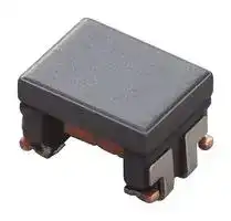


DLW32MH201YK2L
COMMON MODE CHOKE, AEC-Q200, 200UH
- Manufacturer: MURATA
- Product type: SMD Common Mode Chokes / Filters
- SVHC: No SVHC (17-Dec-2015)
- Impedance: -
- Inductance: 200µH
- Product Range: DLW32MH Series
- Product Width: 2.5mm
- Qualification: AEC-Q200
- Product Height: 2.3mm
- Product Length: 3.5mm
- DC Current Rating: 70mA
- DC Resistance Max: 4.1ohm
- Common Mode Filter Case: -
- Inductor Case / Package: -
- Operating Temperature Max: 150°C
- Operating Temperature Min: -55°C
| Delivery and price | |
|---|---|
| Units per pack | 7500 |
| Price | 3.65 € |
| Current stock | 10+ |
| Lead time | 30 days |
## Reference Only

Spec No.: JEFL243C-9128-01 P1/10

## **Wire Wound Chip Common Mode Choke Coil**

## **DLW32MH** □□□ **YK2** □ **Murata Standard Reference Specification** 【 **AEC-Q200** 】

## **1. Scope**

This reference specification applies to Wire Chip Common Mode Choke Coil DLW32MH_YK Series for Automotive Electronics signal line based on AEC-Q200.

## **2. Part Numbering**

(ex) DL W 32 M H 201 Y K 2 L (1) (2) (3) (4) (5) (6) (7) (8) (9) (10)

(1) Chip Common Mode Choke Coil (6) Inductance (2) Structure (W: Winding Type) (7) Circuit (3) Dimension (L × W) (8) Features (4) Type (9) Number of Line

(5) Category (10) Packaging Code  L : Taping (Φ180mm/reel) B : Bulk

∗ Bulk packing also available. (A product is put in the plastic bag under the taping conditions.)

## **3. Rating**

|Customer<br>Part Number|Murata<br>Part Number|Common Mode<br>Inductance<br>(uH)<br>(at 0.1MHz)|Rated<br>Voltage<br>V(DC)|Withstanding<br>Voltage<br>V(DC)|Rated Current (mA)*1|Rated Current (mA)*1|DC<br>Resistance<br>(Ω)|Insulation<br>Resistance<br>(MΩmin.)|ESD Rank|
|---|---|---|---|---|---|---|---|---|---|
||||||Ambient<br>temperature<br>125°C|temperature<br>Ambient<br>temperature<br>150°C||||
||DLW32MH201YK2L 200 (-20%/+30%)|DLW32MH201YK2L 200 (-20%/+30%)|DLW32MH201YK2L 200 (-20%/+30%)<br>80|200|70|5|4.1±20%|10|5B<br>(12kV(AD) <<br>16kV(AD))|


*1 As shown in the diagram below, derating is applied to the rated current based on the operating temperature.

## **4. Standard Testing Condition**

<Unless otherwise specified> Temperature :Ordinary Temperature / 15°C to 35°C Humidity :Ordinary Humidity / 25%(RH) to 85%(RH)

<In case of doubt> Temperature :20°C±2°C Humidity :60%(RH) to 70%(RH) Atmospheric Pressure :86kPa to 106 kPa

MURATA MFG.CO., LTD

Spec No.: JEFL243C-9128-01 P2/10

## Reference Only

## **5. Style and Dimensions**

## ■ **Equivalent Circuits**

**==> picture [8 x 19] intentionally omitted <==**

**----- Start of picture text -----**<br>
5)<br>**----- End of picture text -----**<br>


**==> picture [154 x 65] intentionally omitted <==**

**----- Start of picture text -----**<br>
(1) (2)<br>COR<br>(4) (3)<br>O— — 0 0 0 ——O<br>No polarity<br>**----- End of picture text -----**<br>


## ■ **Unit Mass (Typical value)**

**==> picture [29 x 10] intentionally omitted <==**

**----- Start of picture text -----**<br>
0.06g<br>**----- End of picture text -----**<br>


## **6. Marking**

No Marking.

## **7. Electrical Performance**

|No.|Item|Specification|Test Method|
|---|---|---|---|
|7.1|Common Mode<br>Inductance (Lc)|Meet item 3.|Measuring Equipment : KEYSIGHT 4294A or<br>the equivalent<br>MeasuringFrequency:0.1MHz(ref.item 9.1)|
|7.2|Insulation<br>Resistance(I.R.)|Meet item 3.|Measuring voltage : Rated Voltage<br>Measuringtime : 1 min max.(ref.item 9.3)|
|7.3|Withstanding<br>Voltage|Products shall not be damaged.|Test Voltage : 2.5 times for Rated Voltage<br>Time : 1 to 5 s<br>Charge Current : 1 mA max.(ref.item 9.2)|
|7.4|DC Resistance<br>(Rdc)|Meet item 3.|Measuring current : 10mA max. (ref.item 9.4)<br>(In case of doubt in the above mentioned standard<br>condition, measure by 4 terminal method.)|


## **8.Q200 Requirement**

## **8-1.Performance(based on Table 13 for FILTER EMI SUPPRESSORS/FILTERS) AEC-Q200 Rev.D issued June 1. 2010**

## AEC-Q200

|**AEC-Q200 Rev.D issued June 1. 2010Q200 Rev.D issued June 1. 2010200 Rev.D issued June 1. 2010**|**AEC-Q200 Rev.D issued June 1. 2010Q200 Rev.D issued June 1. 2010200 Rev.D issued June 1. 2010**|**AEC-Q200 Rev.D issued June 1. 2010Q200 Rev.D issued June 1. 2010200 Rev.D issued June 1. 2010**||
|---|---|---|---|
|AEC-Q200-Q200Q200|||Murata Specification / Deviation|
|No.|No.<br>Stress<br>~~a~~|Test Method||
|3 High|3 High<br>Temperature<br>Exposure|1000hours at 150 deg C<br>Set for 24hours<br>at room temperature,<br>then measured.|Meet Table A after testing.<br>Table A<br>Appearance<br>No damage<br>Common Mode<br>Inductance Change<br>(at0.1MHz)<br>Within ±20%|
|4 Temperature Cycling 1000cycles|4 Temperature Cycling 1000cycles|4 Temperature Cycling 1000cycles<br>-55 deg C to +150 deg C<br>Set for 24hours<br>at room temperature,<br>then measured.|Meet Table A after testing.|


MURATA MFG.CO., LTD

~~pO~~ Reference Only

## Spec No.: JEFL243C-9128-01 P3/10

|Spec No.: JEFL243C-9128-01JEFL243C-9128-01-9128-019128-01-0101 P3/10|Spec No.: JEFL243C-9128-01JEFL243C-9128-01-9128-019128-01-0101 P3/10|Spec No.: JEFL243C-9128-01JEFL243C-9128-01-9128-019128-01-0101 P3/10|P3/10|
|---|---|---|---|
|AEC-Q200<br>~~pd~~<br>~~a~~|||Murata Specification / Deviation<br>~~a~~|
|No.<br>~~pd~~<br>~~a~~|No.<br>Stress<br>~~pd~~<br>~~a~~|Test Method<br>~~pd~~<br>~~a~~||
|5 Destructive|5 Destructive<br>Physical Analysis|Per EIA469<br>No electrical tests|Not Applicable|
|7 Biased Humidity|7 Biased Humidity|1000hours at 85 deg C, 85%RH<br>Apply max rated current.<br>Set for 24hours at room<br>temperature,then measured.|Meet Table A after testing.<br>(ref.item 9.5)|
|8 Operational Life<br>~~a~~|8 Operational Life<br>~~a~~|1000hours at 150 deg C<br>Apply max rated current<br>Set for 24hours at room<br>temperature,then measured.<br>~~a~~|Meet Table A after testing.<br>Apply rated current at 150 deg C.<br>(ref.item 9.6) <br>~~a~~|
|9 External Visual<br>~~a~~<br>~~ee~~|9 External Visual<br>~~a~~<br>~~ee~~|Visual inspection<br>~~a~~<br>~~ee~~|No abnormalities<br>~~a~~<br>~~ee~~|
|10 Physical Dimension<br>~~ee~~|10 Physical Dimension<br>~~ee~~|Meet ITEM 5<br>(Style and Dimensions)<br>~~ee~~|No defects<br>~~ee~~|
|12 Resistance<br>~~ee~~|12 Resistance<br>to Solvents<br>~~ee ~~|Per MIL-STD-202 Method 215<br> ~~ee ~~|Not Applicable<br> ~~ee~~|
|13  Mechanical Shock|13  Mechanical Shock|Per MIL-STD-202 Method 213<br>Condition F:<br>1500g's(14.7N)/0.5ms/Half sine|Meet TableAafter testing.|
|14 Vibration|14 Vibration|5g's(0.049N) for 20 minutes,<br>12cycles each of 3 oritentations<br>Test from 10-2000Hz.|Meet Table A after testing.|
|15 Resistance|15 Resistance<br>to Soldering Heat|No-heating<br>Solder temperature<br>260C+/-5 deg C<br>Immersion time 10s|Pre-heating:150 to 180C / 90±30s<br>Meet Table A after testing.<br>The ferrite plates shall be supported so as not to be<br>dipped in solder bath.<br>||Tweezer<br>Tent?|
|17 ESD<br>~~ee~~|17 ESD<br>~~ee~~|Per AEC-Q200-002<br>~~ee~~|ESD Rank: Meet Item 3 (Rating)<br>Meet Table A after testing.<br>~~ee~~|
|18 Solderability|18 Solderability|Per J-STD-002|Method b : Not Applicable<br>More than 95% of the external electrodes (diagonal part<br>of the figure) should be covered with new solder.<br>Flux:Ethanol solution of rosin,25(wt)% includes activator<br>equivalent to 0. 06 to 0.10(wt)% chlorine<br>The side electrode is 0.2 mm from the bottom.<br>The ferrite plates shall be supported so as not to be<br>dippedinsolderbath.<br>gei IP<br>|Tweezer<br>ueif|
|19 Electrical|19 Electrical<br>Characterization|Measured:<br>Common mode inductance|No defects|


MURATA MFG.CO., LTD

Reference Only

Spec No.: JEFL243C-9128-01 P4/10

|Spec No.: JEFL243C-9128-01JEFL243C-9128-01-9128-019128-01-0101 P4/10|Spec No.: JEFL243C-9128-01JEFL243C-9128-01-9128-019128-01-0101 P4/10|Spec No.: JEFL243C-9128-01JEFL243C-9128-01-9128-019128-01-0101 P4/10|P4/10|
|---|---|---|---|
|AEC-Q200|||Murata Specification / Deviation|
|No.|Stress|Test Method||
|20 Flammability|20 Flammability|Per UL-94|Not Applicable|
|21 Board Flex|21 Board Flex|Epoxy-PCB(1.6mm)<br>Deflection 2mm(min)<br>Holdingtime 60s|Meet Table A after testing.|
|22 Terminal Strength|22 Terminal Strength|Per AEC-Q200-006<br>A force of 17.7N for 60s|No defects|
|30 Electrical<br>Transient<br>Conduction|30 Electrical<br>Transient<br>Conduction|Per ISO-7637-2|Not Applicable|


## **9. Terminal to be Tested.**

When measuring and supplying the voltage, the following terminal is applied.

||No.|Item||||||||Terminal to be Tested|Terminal to be Tested|Terminal to be Tested|Terminal to be Tested|Terminal to be Tested|Terminal to be Tested|Terminal to be Tested|Terminal to be Tested||
|---|---|---|---|---|---|---|---|---|---|---|---|---|---|---|---|---|---|---|
||9.1|Common Mode Inductance<br>(Measurement Terminal)|||||Terminal|of|~~bree~~<br>~~| fe~~|||||||||Terminal|
||||||||||||||||||||
||9.2|Withstanding Voltage|||||||||||||||||
|||(Measurement Terminal)|||||Terminal||||||||||||
|9.3<br>Insulation Resistance<br>(Measurement Terminal)<br>~~Pf~~|||||||Terminal||||:||||;||||
||9.4|DC Resistance|||||Terminal|||||||||||Terminal|
|||(Measurement Terminal)||||||||||iy||||:|||
||||||||||||||||||||
||||||||||||||||||||
||||||||||||||||||||
||||||||||||||||||||
|||||||||||||iy|||:||||
||||||||Terminal|||||||||||Terminal|
||||||||||||||||||||
|9.5<br>Biased Humidity<br>(Supply Terminal)<br>~~—~~|||||||Terminal||||||||||||
||9.6|Operational Life|||||Terminal||||||||||||
|||(SupplyTerminal)|||||||||||||||||
|**10. P.C.B., Flux, Solder and Soldering condition**|**10. P.C.B., Flux, Solder and Soldering condition**||**10. P.C.B., Flux, Solder and Soldering condition**||||||||||||||||
||Test shall be done using P.C.B., Flux, Solder and Soldering condition which are specified in item 13 except|||Test shall be done using P.C.B., Flux, Solder and Soldering condition which are specified in item 13 except||Test shall be done using P.C.B., Flux, Solder and Soldering condition which are specified in item 13 except||Test shall be done using P.C.B., Flux, Solder and Soldering condition which are specified in item 13 except|||||||||||
||the case of being specified special condition.||the case of being specified special condition.|||the case of being specified special condition.|||||||||||||
|**11. Specification of Packaging**|**11. Specification of Packaging**|**11. Specification of Packaging**|||||||||||||||||
|**11.1 Appearance and Dimensions ( 12mm-wide,Plastic tape)**|**11.1 Appearance and Dimensions ( 12mm-wide,Plastic tape)**|**11.1 Appearance and Dimensions ( 12mm-wide,Plastic tape)**|||||||||||||||||
|||2.0+0.1||||||||2,640.1|||||||||
||4.0+0.1||_|<br>4.0401||01.520"!|||(0.3)||||||||||||
||I<br>|<br>|<br>I<br>nelneen||||3}<br>+H<br>a)||S| <br> RI|e<br>;<br> Fg|||of|||*****Dimension of the Cavity is measured<br>at the bottom side.<br>“Dir||||||


## **10. P.C.B., Flux, Solder and Soldering condition**

Test shall be done using P.C.B., Flux, Solder and Soldering condition which are specified in item 13 except the case of being specified special condition.

## **11. Specification of Packaging**

## **11.1 Appearance and Dimensions ( 12mm-wide,Plastic tape)**

MURATA MFG.CO., LTD

Reference Only

Spec No.: JEFL243C-9128-01 P5/10

## **11.2. Specification of Taping**

- (1) Packing quantity (Standard quantity) φ 180 mm reel :1500 pcs. / reel

- (2) Packing Method

- Products shall be packaged in each embossed cavity of plastic tape and sealed with cover tape.

- (3) Sprocket Hole

The sprocket holes are to the right as the tape is pulled toward the user.

- (4) Spliced point

The cover tape have no spliced point.

- (5) Missing components number

Missing components number within 0.1% of the number per reel or 1 pc., whichever is greater, and are not continuous. The specified quantity per reel is kept.

## **11.3. Pull Strength of Plastic Tape**

|Plastic Tape||5 N min.||||
|---|---|---|---|---|---|
|Cover Tape||10 N min.||||
|**11.4. Peeling off force of Cover Tape**<br>0.2N to 0.7N (minimum value is typical.)<br>Speed of Peeling off : 300 mm / min<br>165 to 180 degree||||F<br>_———.|Cover tape|
|**11.5. Dimensions of Leader-tape, Trailer and Reel**|**11.5. Dimensions of Leader-tape, Trailer and Reel**|**11.5. Dimensions of Leader-tape, Trailer and Reel**|||Plastic tape|


## **11.4. Peeling off force of Cover Tape**

0.2N to 0.7N (minimum value is typical.) Speed of Peeling off : 300 mm / min

## **11.5. Dimensions of Leader-tape, Trailer and Reel**

There shall be leader-tape (cover tape only and empty tape) and trailer-tape (empty tape) as follows. « Packaging Code : L (Φ180mm reel) »

## **11.6 Marking for reel**

- Customer part number **,** MURATA part number, Inspection number( ∗ 1), RoHS Marking( ∗ 2), Quantity, etc ∗ 1) « Expression of Inspection No. » □□ OOOO ××× (1) (2) (3)

(1) Factory Code (2) Date First digit : Year / Last digit of year Second digit : Month / Jan. to Sep. → 1 to 9, Oct. to Dec. → O, N, D Third, Fourth digit : Day (3) Serial No. ∗ 2) « Expression of RoHS Marking » ROHS – Y ( △ ) (1) (2)

(1) RoHS regulation conformity parts.

- (2) MURATA classification number

## **11.7 Marking for Outside package**

Customer name Purchasing Order Number, Customer Part Number, MURATA part number, RoHS Marking( ∗ 2), Quantity, etc

MURATA MFG.CO., LTD

Reference Only

Spec No.: JEFL243C-9128-01 P6/10

## **11.8 Specification of Outer Case**

|H|H|||Reel<br>Outer Case Dimensions<br>(mm)<br>Standard Reel<br>Quantity in<br>Outer Case<br>(Reel)<br>W<br>D<br>H<br>φ180mm<br>186<br>186<br>93<br>4<br>*Above Outer Case size is typical. It depends on a quantity of an order.<br>D<br>Label|Reel<br>Outer Case Dimensions<br>(mm)<br>Standard Reel<br>Quantity in<br>Outer Case<br>(Reel)<br>W<br>D<br>H<br>φ180mm<br>186<br>186<br>93<br>4<br>*Above Outer Case size is typical. It depends on a quantity of an order.<br>D<br>Label|
|---|---|---|---|---|---|
|||||||
|||||D||
|||||||
|||W||||


## **12.** △ **! Caution**

## **12.1 Mounting Direction**

Mount products in right direction.

Wrong direction which is 90 ° rotated from right direction causes not only open or short circuit but also flames or other serious trouble.

**==> picture [177 x 50] intentionally omitted <==**

**----- Start of picture text -----**<br>
Z Z<br>right direction wrong direction<br>**----- End of picture text -----**<br>


## **12.2 Limitation of Applications**

Please contact us before using our products for the applications listed below which require especially high reliability for the prevention of defects which might directly cause damage to the third party's life, body or property.

(1) Aircraft equipment

- (2) Aerospace equipment

- (3) Undersea equipment

(4) Power plant control equipment

- (5) Medical equipment

(6) Transportation equipment (trains, ships, etc.)

- (7) Traffic signal equipment

- (8) Disaster prevention / crime prevention equipment

(9) Data-processing equipment

- (10) Applications of similar complexity and /or reliability requirements to the applications listed in the above

## **12.3 Caution(Rating)**

Do not exceed maximum rated current of the product. Thermal stress may be transmitted to the product and short/open circuit of the product or falling off the product may be occurred.

## **12.4 Fail-safe**

Be sure to provide an appropriate fail-safe function on your product to prevent a second damage that may be caused by the abnormal function or the failure of our product.

## **13. Notice**

Products can only be soldered with reflow.

This product is designed for solder mounting.

Please consult us in advance for applying other mounting method such as conductive adhesive.

## **13.1 Flux and Solder**

|Flux|Use rosin-based flux,(with converting chlorine content 0.06 to 0.1(wt)%. ),<br>but not highly acidic flux<br>(with Halogen content exceeding 0.2(wt)% conversion to chlorine).<br>Donot usewater-solubleflux.|
|---|---|
|Solder|Use Sn-3.0Ag-0.5Cu solder<br>Standardthickness of the solderpaste should be150µm.|


## **13.2 Assembling**

<Exclusive use of Reflow soldering>

Flow soldering may cause deterioration in insulation resistance. So, reflow soldering shall be applied for this product.

## **13.3 Cleaning Conditions**

Do not clean after soldering. Some cleaning agents may degrade bonding strength,and characteristics of products by detaching. If cleaning,please contact us.

## **13.4 Resin coating (moistureproof coating)**

Please avoid resin coating the product because there is a possibility of disconnection.

MURATA MFG.CO., LTD

Reference Only

Spec No.: JEFL243C-9128-01 P7/10

## **13.5 Attention regarding P.C.B. bending**

The following shall be considered when designing and laying out P.C.B.'s.

(1) P.C.B. shall be designed so that products are not subject to the mechanical stress due to warping the board.

## [ Products direction ]

**==> picture [155 x 47] intentionally omitted <==**

**----- Start of picture text -----**<br>
a<br>b<br>〈 Poor example 〉 〈 Good example 〉<br>**----- End of picture text -----**<br>


Products shall be location the sideways Direction (Length : a<b) to the mechanical Stress.

## (2) Components location on P.C.B. separation.

It is effective to implement the following measures, to reduce stress in separating the board. It is best to implement all of the following three measures; however, implement as many measures as possible to reduce stress.

|Contents of Measures|Stress Level||
|---|---|---|
|(1) Turn the mounting direction of the component parallel to the board separation|A > D *1||
|surface.|||
|(2)Add slits in the board separationpart.|A > B||
|(3) Keep the mounting position of the component away from the board separation|A > C||
|surface.|||
|*1 A > D is valid when stress is added vertically to<br>Perforation<br>B<br>C|the perforation as||
|with Hand Separation.<br>If a Cutting Disc is used, stress will be diagonal to the PCB, therefore<br>A > D is invalid.<br>Slit<br>A<br>D|||


If a Cutting Disc is used, stress will be diagonal to the PCB, therefore A > D is invalid.

- (3) Mounting Components Near Screw Holes

When a component is mounted near a screw hole, it may be affected by the board deflection that occurs during the tightening of the screw. Mount the component in a position as far away from the screw holes as possible.

**==> picture [120 x 32] intentionally omitted <==**

**----- Start of picture text -----**<br>
Screw Hole Recommended<br>**----- End of picture text -----**<br>


**==> picture [176 x 265] intentionally omitted <==**

**----- Start of picture text -----**<br>
Portion of<br>Perforation<br>×<br>P.C.B .<br>○<br>○<br>Product<br>Portion of ×<br>Perforation<br>P.C.B . ○ ×<br>Product<br>Hole<br>Pick-up nozzle<br>Product<br>P.C.B.<br>Support pin<br>**----- End of picture text -----**<br>


## **13.6 Attention Regarding P.C.B. Design**

- < The Arrangement of Products >

- P.C.B. shall be designed so that products are far from the portion of perforation.

The portion of perforation shall be designed

as narrow as possible, and shall be designed so as not to be applied the stress in the case of P.C.B. separation.

Products shall not be arranged on the line of a series of holes when there are big holes in P.C.B. (Because the stress concentrate on the line of holes.)

## < Products Placing >

Support pins shall be set under P.C.B .

to prevent causing a warp to P.C.B.

during placing the products on the other side of P.C.B.

- < P.C.B. Separation >

   - P.C.B. shall not be separated with hand.

   - P.C.B. shall be separated with the fixture so as not to cause P.C.B. bending.

MURATA MFG.CO., LTD

Reference Only

Spec No.: JEFL243C-9128-01 P8/10

## **13.7 Standard Land Dimensions (Reflow)**

**==> picture [109 x 82] intentionally omitted <==**

**----- Start of picture text -----**<br>
*1<br>*2<br>**----- End of picture text -----**<br>


- ∗ 1 If the pattern is made with less than 0.4mm , in the worst case , short circuit between lines may be occurred due to the spread of soldering paste or mount placeing accuracy.

- ∗ 2 If the pattern is made with wider, the strength of bending will be reduced. Moreover, if the pattern is made with less than 2mm , in the worst case short circuit may be occurred.

- ∗ 3 Do not use gilded pattern. A copper wire may cause open by dissolution of metallization.

## **13.8 Standard Soldering Condition**

- 1.Reflow Soldering

- (1) Standard printing pattern of solder paste

- Standard thickness of the solder paste should be 150 µm.

- Use the solder paste printing pattern of the right pattern.

- For the resist and copper foil pattern, use standard land dimensions.

- Use the Solder Sn-3.0Ag-0.5Cu for pattern printing.

- Spread of soldering paste between lines may cause short circuit of lines. (in mm)

## (2) Soldering Temperature

Temperature difference between soldering and surface of components must be within 150°C, in preheating. When components are immersed in liquid after soldering, temperature difference should be within 100°C. If preheating is not enough, components may be cracked and cause deterioration in insulation resistance.

- (3) Soldering Condition

Standard soldering profile and the limit soldering profile is as follows.

The excessive limit soldering conditions may cause leaching of the electrode and / or resulting in the eterioration of product quality.

MURATA MFG.CO., LTD

~~ot~~ Reference Only Spec No.: JEFL243C-9128-01 P9/10

Soldering Profile for Lead Free solder (Sn-3.0Ag-0.5Cu solder )

**==> picture [353 x 254] intentionally omitted <==**

**----- Start of picture text -----**<br>
Temp. 260℃<br>( ℃)<br>245℃±3℃<br>230℃<br>220℃<br>Limit Profile<br>180<br>150<br>30s ~60 s Standard Profile<br>60s max.<br>90s±30s Time. ( s)<br>LP<br>Standard Profile  Limit Profile<br>Pre-heating 150~180°C  、90s±30s<br>Heating above 220°C、30s~60s  above 230°C、60s max.<br>Peak temperature  245±3°C  260°C,10s<br>Cycle of reflow  2 times  2 times<br>**----- End of picture text -----**<br>


## 2. Reworking with Soldering iron

The following conditions must be strictly followed when using a soldering iron after being mounted by reflow soldering.

- Pre-heating: 150°C, 1 min          · Soldering iron output: 30W max.

- Tip temperature: 350°C max.        · Tip diameter:φ3mm max.

- Soldering time : 3(+1,-0) s.          · Times : 2times max.

Notes : Do not touch the products directly with the soldering iron.

## 3. Solder Volume

Solder shall be used not to be exceeded the upper limits as shown below.

Accordingly increasing the solder volume, the mechanical stress to Chip is also increased. Exceeding solder volume may cause the failure of mechanical or electrical performance. In case if the solder volume is much, we recommend to make the size of the solder paste with less than the land pattern.

- 4.Solder fillet

Solder fillet in lateral direction is not formed in some case because of product's structure, but it is not something that affects product's performance and reliability.

MURATA MFG.CO., LTD

~~PO~~ Reference Only Spec No.: JEFL243C-9128-01 P10/10

## **13.9 Caution for use**

・ When you hold products with a tweezer, please hold like a figure of the right side, and sharp material, such as a pair of tweezers, shall not be touched to the winding portion to prevent the breaking of wire.

- ・ Mechanical shock should not be applied to the products

mounted on the board to prevent the breaking of the core.

## **13.10 Handling of a substrate**

After mounting products on a substrate, do not apply any stress to the product caused by bending or twisting to the substrate when cropping the substrate, inserting and removing a connector from the substrate or tightening screw to the substrate.

Excessive mechanical stress may cause cracking in the product.

Bending                         Twisting

## **13.11 Brushing of neighborhood of products**

When you clean the neighborhood of products such as connector pins, bristles of cleaning brush shall not be touched to the winding portion to prevent the breaking of wire.

## **13.12 Mounting Conditions**

- ・Please check the mounting condition before using.

- ・Using mounting conditions (nozzles, equipment conditions, etc.) that are not suitable for products may lead to pick up errors, misalignment, or damage to the product.

## **13.13 Operating Environment**

Do not use this product under the following environmental conditions, on deterioration of the performance, such as insulation resistance may result from the use.

(1) in corrosive gases (acidic gases, alkaline gases, chlorine, sulfur gases, organic gases and etc.)

(2) in the atmosphere where liquid such as organic solvent, may splash on the products.

## **13.14 Storage Condition**

- (1) Storage period

Use the products within 12 months after delivered.

Solderability should be checked if this period is exceeded.

- (2) Storage environment conditions

   - ·Products should be stored in the warehouse on the following conditions.

Temperature : -10 ~ +40°C

Humidity : 15 to 85% relative humidity  No rapid change on temperature and humidity.

- Products should not be stored in corrosive gases, such as sulfureous, acid gases, alkaline gases, to prevent the following deterioration.

Poor solderability due to the oxidized electrode.

   - Products should be stored on the palette for the prevention of the influence from humidity,dust and so on.

   - Products should be stored in the warehouse without heat shock, vibration, direct sunlight and so on.

   - Products should not be stored under the air tights packaged condition.

- (3) Delivery

Care should be taken when transporting or handling product to avoid excessive vibration or mechanical shock.

## **14.** △ **! Note**

(1)Please make sure that your product has been evaluated in view of your specifications with our product being mounted to your product.

(2)You are requested not to use our product deviating from the reference specifications.

(3)The contents of this reference specification are subject to change without advance notice. Please approve our product specifications or transact the approval sheet for product specifications before ordering.

MURATA MFG.CO., LTD
Updated at June 10, 2026
Established in Kyoto in 1944, Murata has grown into a global leader in the design and manufacture of advanced electronic components, specializing in ceramic passive components, wireless connectivity modules, and power conversion technologies. Renowned for its foundational work in materials science and process innovation, Murata delivers solutions that drive the evolution of modern electronics across telecommunications, mobility, industrial, and healthcare applications. This extensive portfolio is anchored by a broad selection of high-performance passive components, heavily focused on inductive solutions. Engineers can choose from hundreds of specialized RF inductors and power inductors engineered for exceptional reliability, efficiency, and miniaturization. The range also features robust EMC and RFI suppression solutions, highlighted by industry-leading common mode chokes and power line filters designed to ensure signal integrity and strict regulatory compliance in demanding circuit environments. Beyond inductive and filtering components, the offering encompasses a comprehensive array of critical circuit protection, timing, and power devices. Murata's precision NTC and PTC thermistors provide essential temperature sensing and thermal management, while its robust lineup of ceramic resonators and quartz crystals ensures highly accurate frequency control. Supported by premium non-rechargeable batteries, polymer capacitors, and advanced sensing transducers, Murata equips designers with the versatile building blocks required for next-generation technological development.
About Novapart
Novapart is a B2B electronic component broker specialising in stock shortages and cost reduction. We source hard-to-find parts and identify compliant alternatives across a catalogue of 410,000+ components from 500+ manufacturers.
Learn more →Stock Shortage Specialist
When a component is unavailable, discontinued or has an unacceptable lead time, we tap into our network of vetted European and Asian distributors to source what you need — without compromising on quality or traceability.
Request a quote →Compliant Alternatives
We identify pin-to-pin, electrically equivalent substitutes that meet the same certifications (RoHS, AEC-Q100, REACH) as your original specification — validated against datasheets, not just part numbers. Often at a lower cost.
BOM Analysis service →