
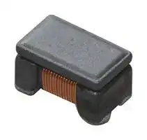


DLW21PH201XQ2L
Choke, Common Mode, AEC-Q200, 500 mA, 200 ohm, 2 mm L x 1.2 mm W x 1.2 mm H
- Manufacturer: MURATA
- Product type: SMD Common Mode Chokes / Filters
- SVHC: No SVHC (04-Feb-2026)
- Impedance: 200ohm
- Inductance: -
- Product Range: DLW21PH Series
- Product Width: 1.2mm
- Qualification: AEC-Q200
- Product Height: 1.2mm
- Product Length: 2mm
- DC Current Rating: 500mA
- DC Resistance Max: 0.14ohm
- Inductor Case / Package: -
- Operating Temperature Max: 125°C
- Operating Temperature Min: -40°C
| Delivery and price | |
|---|---|
| Units per pack | 2000 |
| Price | 0.205 € |
| Current stock | 10+ |
| Lead time | 30 days |
P1/10 Spec No.:JEFL243C-9130-01 ## **Chip Common Mode Choke Coil DLW21PH□□□XQ2□ REFERENCE SPECIFICATION - Murata Standard Specification [AEC Q200]** ## **1. Scope** This reference specification applies to Chip Common Mode Choke Coil DLW21PH□□□XQ2□ series for automotive electronics based on AEC-Q200. ## **2. Part Numbering** (Ex.) |(Ex.)|||||||||||||||| |---|---|---|---|---|---|---|---|---|---|---|---|---|---|---|---| |DL||W||21||PH||201||X|Q||2||L| |Product ID||Type||Dimension|Dimension|Application and||Impedan||Performance|Category||Number||Packaging| |||||(L × W)||characteristic||ce|||||of line||L: taping| |||||||H:for automotive|||||||||*B: bulk| |||||||electronics|||||||||| *B: Bulk packing is also available. (The product sealed on the carrier tape is stored in a plastic bag.) ## **3. Part Number and Rating** Operating temperature range -40°C to +125°C Storage temperature range -40°C to +125°C |||||||Rated Current*|Rated Current*|Rated Current*| |---|---|---|---|---|---|---|---|---| |Customer<br>Part number|Murata<br>Part number|Common mode<br>impedance (Ω)<br>at 100 MHz<br>Rated<br>voltage<br>(VDC)||Withstanding<br>Voltage<br>(VDC)||(mA)<br>Ambient<br>temperature<br>Ambient<br>temperature||| |||||||105°C||125°C| ||DLW21PH201XQ2L|200±25%|200±25%<br>20||50|500||350| |||||||||| |Murata<br>Part number|DC<br>resistance<br>(Ω)<br>Insulation<br>resistance(MΩ min.)||ESD rank|||||| |DLW21PH201XQ2L<br>0.14±20%<br>10<br>5B<br>~~ee~~||||||||| * As shown in the diagram below, derating is applied to the rated current based on the operating temperature ESD Rank Maximum Withstand Voltage 5B 12,000 V (AD) to < 16,000 V (AD) ## **4. Testing Conditions** |**4. Testing Conditionsg Conditions Conditions**|| |---|---| |Unless otherwise specified|Temperature: ordinary temperature (15°C to 35°C)<br>Humidity: ordinaryhumidity [25% to 85%(RH)]| |In case of doubt|Temperature: 20°C±2°C<br>Humidity: 60% to 70% (RH)<br>Atmosphericpressure: 86 kPa to 106 kPa| MURATA MFG CO., LTD P2/10 Spec No.:JEFL243C-9130-01 ## **5. Appearance and Dimensions** ■ Equivalent Circuit Unit mass (typical value): 0.011 g ## **6. Marking** No marking. ## **7. Electrical Performance** |No.|Item|Specification|Test method| |---|---|---|---| |7.1|Common Mode<br>Impedance|Meet chapter 3 ratings.|Measuring equipment: Keysight 4991A or the<br>equivalent<br>Measuring frequency: 100±1 MHz<br>Measuring method: see "Measuring method" in the<br>chapter "Appendix".| |7.2|Withstanding<br>Voltage|Products shall not be damaged.|Test Voltage : 2.5 times for Rated Voltage<br>Time : 1 to 5 seconds<br>Charge Current : 1 mA max.<br>Measuring method: see "Measuring method" in the<br>chapter "Appendix".| |7.3 DC resistance|7.3 DC resistance|Meet chapter 3 ratings.|Measuring current : 100 mA max.<br>(In case of doubt in the above mentioned standard<br>condition, measure by 4 terminal method.)<br>Measuring method: see "Measuring method" in the<br>chapter "Appendix".| |7.4 Insulation|7.4 Insulation<br>Resistance|Meet chapter 3 ratings.|Measuring equipment: Advantest R8340A or the<br>equivalent<br>Measuring voltage : Rated Voltage<br>Measuring time : 60 seconds max.<br>Measuring method: see "Measuring method" in the<br>chapter "Appendix".| MURATA MFG CO., LTD P3/10 |**AEC-Q200 Rev.D issued June 1. 2010**<br>|**AEC-Q200 Rev.D issued June 1. 2010**<br>|**AEC-Q200 Rev.D issued June 1. 2010**<br>|| |---|---|---|---| |AEC-Q200<br>~~>~~|||Murata Specification / Deviation| |No.<br>~~>~~|No.<br>Stress<br>~~>~~|Test Method<br>~~>~~|| |3 High temperature<br>~~>~~|3 High temperature<br>exposure<br>~~>~~|1000 h at 125°C<br>Set for 24 h at room condition,<br>then measured.<br>~~>~~|Set for 24 h at room condition,<br>Appearance: No damage<br>Common mode impedance change rate: within ±20%<br>Insulation resistance: 10 MΩ min.<br>DC resistance change rate: within ±30%| |4 Temperature cycling<br>~~rn~~|4 Temperature cycling<br>~~rn~~|1000 cycles<br>-40°C to +125°C<br>Set for 24 h at room condition<br>then measured.<br>|Appearance: No damage<br>Common mode impedance change rate: within ±20%<br>Insulation resistance: 10 MΩ min.<br>DC resistance change rate: within ±30%<br>| |5 Destructive physical<br>~~rn~~|5 Destructive physical<br>analysis<br>~~rn~~|Per EIA469<br>No electrical tests<br>|Not applicable<br>| |7 Biased humidity<br>~~rn~~|7 Biased humidity<br>~~rn~~|1000 h at 85°C, 85% (RH).<br>Apply max rated voltage and<br>rated current.<br>Set for 24 h at room condition,<br>then measured.<br>|Apply max rated current.<br>Appearance: No damage<br>Common mode impedance change rate: within ±20%<br>Insulation resistance: 10 MΩ min.<br>DCresistance changerate: within ±30%<br>| |8 Operational life<br>~~rnfof~~|8 Operational life<br>~~rnfof~~|Apply 125°C 1000 h<br>Set for 24 h at room condition<br>then measured.<br>~~fof~~|Appearance: No damage<br>Common mode impedance change rate: within ±20%<br>Insulation resistance: 10 MΩ min.<br>DC resistance change rate: within ±30%<br>~~fof~~| |9 External visual<br>~~fof~~|9 External visual<br>~~fof~~|Visual inspection<br>~~fof~~|No abnormalities<br>~~fof~~| |10 Physical dimension<br>~~a~~|10 Physical dimension<br>~~a~~|Meet chapter 5, "Appearance<br>and Dimensions".<br>~~a~~|No defects<br>~~a~~| |12 Resistance to<br>~~ee~~|12 Resistance to<br>solvents<br>~~ee~~|Per MIL-STD-202<br>Method 215<br>~~ee~~|Not applicable<br>~~ee~~| |13 Mechanical shock<br>~~ee~~|13 Mechanical shock<br>~~ee~~|Per MIL-STD-202<br>Method 213<br>Condition F:<br>1500g's/0.5 ms/half sine<br>~~ee~~|Appearance: No damage<br>Common mode impedance change rate: within ±20%<br>Insulation resistance: 10 MΩ min.<br>DC resistance change rate: within ±30%<br>~~ee~~| |14 Vibration<br>~~a~~|14 Vibration<br>~~a~~|5 g's for 20 min, 12 cycles each<br>of 3 orientations<br>Test from 10 Hz to 2000 Hz<br>~~a~~|5 g's for 20 min, 12 cycles each<br>Appearance:No damage<br>Common mode impedance change rate: within ±20%<br>~~a~~| |15 Resistance<br>~~a~~|15 Resistance<br>to Soldering Heat<br>~~a~~|No-heating<br>Solder temperature<br>260°C±5°C<br>Immersion time 10 s<br>~~a~~|Appearance: No damage<br>Common mode impedance change rate: within ±20%<br>Insulation resistance: 10 MΩ min.<br>DC resistance change rate: within ±30%<br>Deviation for AEC-Q200<br>Pre-heating: 150°C/60s<br>~~a~~| |17 ESD|17 ESD|Per AEC-Q200-002|ESD Rank: Refer to chapter 3, "Part Number and Rating"<br>Appearance: No damage<br>Common mode impedance change rate: within ±20%<br>Insulation resistance: 10 MΩ min.<br>DC resistance change rate: within ±30%| |18 Solderability|18 Solderability|Per J-STD-002|95% or more of the outer electrode shall be covered<br>with new solder seamlessly.<br>(except exposed wire)<br>Deviation for AEC-Q200<br>Method b: Not applicable<br>Pre-heating: 150°C/60s| |19 Electrical<br>~~a~~|19 Electrical<br>Characterization<br>~~a~~|Measured:<br>common mode impedance<br>~~a~~<br>~~a~~|No defects<br>~~a~~| |20 Flammability<br>~~re~~|20 Flammability<br>~~re~~|Per UL-94<br>~~re~~|Not applicable<br>~~re~~| |21 Board Flex<br>~~re~~<br>~~re~~|21 Board Flex<br>~~re~~<br>~~re~~|Epoxy-PCB (1.6 mm)<br>Deflection 2 mm (min.)<br>60 s minimum holding time<br>~~re~~<br>~~ee~~|Appearance:No damage<br>Common mode impedance change rate: within ±20%<br>Deviation for AEC-Q200<br>Epoxy-PCB thickness: 1.0 mm<br>~~re~~<br>~~ee~~| |22 Terminal Strength<br>~~re~~|22 Terminal Strength<br>~~re~~|Per AEC-Q200-006<br>A force of 17.7 N for 60 s<br>~~ee~~|Appearance: No damage<br>Deviation for AEC-Q200<br>Applyingforce: 10 N<br>~~ee~~| |30 Electricalcharacterization<br>~~re~~<br>~~a~~|30 Electricalcharacterization<br>conduction<br>~~re~~<br>~~a~~|30 Electricalcharacterization<br>Per ISO-7637-2<br>~~ee~~<br>~~a~~|Not applicable<br>~~ee~~<br>~~a~~| MURATA MFG CO., LTD P4/10 Spec No.:JEFL243C-9130-01 ## **9. Specification of Packaging** ## **9.1 Appearance and dimensions of tape (8 mm width/plastic tape)** |A|(1.45)| |---|---| |B|(2.25)| |t|(1.4)| |t'|(0.25)| * The dimensions of the cavity are measured at its bottom. ## **9.2 Taping specifications** |Packing<br>quantity<br>(Standardquantity)|2000 pcs/reel| |---|---| |Packing method|The products are placed in cavities of a carrier tape and sealed by a cover tape (top tape and<br>bottom tape when the cavities of the carrier tape arepunched type).| |Feed hole position|The feed holes on the carrier tape are on the right side when the cover tape (top tape when the<br>cavities of the carrier tape arepunched type)ispulled toward the user.| |Joint|The carrier tape and cover tape (top tape when the cavities of the carrier tape are punched type)<br>are seamless.| |Number of missing<br>products|Number of missing products within 0.025% of the number per reel or 1 pc., whichever is greater,<br>and are not continuous. The specifiedquantity per reel is kept.| ## **9.3 Break down force of tape** |**9.3 Break down force of tapepee **|| |---|---| |Cover tape(or toptape)|5 N min.| |Bottom tape(onlywhen the cavities of the carrier tape arepunched type)|5 N min.| MURATA MFG CO., LTD P5/10 Spec No.:JEFL243C-9130-01 ## **9.4 Peeling off force of tape** Speed of peeling off 300 mm/min Peeling off force 0.1 N to 0.7 N (The lower limit is for typical value.) ## **9.5 Dimensions of leader section, trailer section and reel** A vacant section is provided in the leader (start) section and trailer (end) section of the tape for the product. The leader section is further provided with an area consisting only of the cover tape (or top tape). (See the diagram below.) ## **9.6 Marking for reel** Customer part number, Murata part number, inspection number (*1), RoHS marking (*2), quantity, etc. |*1 Expression of inspection No.:<br>□□<br>○○○○<br><br>(1)<br>(2)<br>(3)|*1 Expression of inspection No.:<br>(1) Factory code<br>(2) Date<br>First digit: year/last digit of year<br>Second digit: month/Jan. to Sep.→1 to 9, Oct. to Dec.→O, N, D<br>Third, Fourth digit: day<br>(3)Serial No.| |---|---| |*2 Expression of RoHS marking:<br>ROHS-<br>Y<br>()<br>(1)<br>(2)|(1) RoHS regulation conformity<br>(2) Murata classification number| ## **9.7 Marking on outer box (corrugated box)** Customer name, purchasing order number, customer part number, Murata part number, RoHS marking (*2), quantity, etc. ## **9.8 Specification of outer box** |||||||||Dimensions of outer box|Dimensions of outer box|Dimensions of outer box|| |---|---|---|---|---|---|---|---|---|---|---|---| |||||||Label||(mm)<br>W<br>D||H|Standard reel quantity<br>in outer box (reel)| |H||||||||186<br>186||93|5| ||||||D||* Above outer box size is typical. It depends on a|* Above outer box size is typical. It depends on a||* Above outer box size is typical. It depends on a|| |||W||||||quantityof an order.||of an order.|| MURATA MFG CO., LTD P6/10 Spec No.:JEFL243C-9130-01 ## **10. Caution** ## **10.1 Restricted applications** Please contact us before using our products for the applications listed below which require especially high reliability for the prevention of defects which might directly cause damage to the third party's life, body or property. (1) Aircraft equipment (2) Aerospace equipment (3) Undersea equipment - (4) Power plant control equipment - (5) Medical equipment - (6) Transportation equipment (trains, ships, etc.) - (7) Traffic signal equipment - (8) Disaster/crime prevention equipment - (9) Data-processing equipment - (10) Applications of similar complexity and/or reliability requirements to the applications listed in the above ## **10.2 Precautions on rating** Avoid using in exceeded the rated temperature range, rated voltage, or rated current. Usage when the ratings are exceeded could lead to wire breakage, burning, or other serious fault. ## **10.3 Inrush current** If an inrush current (or pulse current or rush current) that significantly exceeds the rated current is applied to the product, overheating could occur, resulting in wire breakage, burning, or other serious fault. ## **10.4 Fail-safe** Be sure to provide an appropriate fail-safe function on your product to prevent a second damage that may be caused by the abnormal function or the failure of our product. ## **10.5 Mounting direction** Mount the products in the correct direction. Mounting in a direction that is rotated 90° from the correct direction could result in an open or short circuit, and in some cases, burning or other serious accident could also occur. ## **11. Precautions for Use** This product is for use only with reflow soldering. It is designed to be mounted by soldering. If you want to use other mounting method, for example, using a conductive adhesive, please consult us beforehand. Also, if repeatedly subjected to temperature cycles or other thermal stress, due to the difference in the coefficient of thermal expansion with the mounting substrate, the solder (solder fillet part) in the mounting part may crack. The occurrence of cracks due to thermal stress is affected by the size of the land where mounted, the solder volume, and the heat dissipation of the mounting substrate. Carefully design it when a large change in ambient temperature is assumed. ## **11.1 Land dimensions** The following diagram shows the recommended land dimensions for reflow soldering. |a|0.8| |---|---| |b|2.6| |c|0.4| |d|1.2| Do not use gilded pattern. A copper wire may cause open by dissolution of metallization. MURATA MFG CO., LTD P7/10 ~~oe~~ Spec No.:JEFL243C-9130-01 ## **11.2 Flux and solder used** |**11.2 Flux and solder used**|**11.2 Flux and solder used**| |---|---| |Flux|• Use a rosin-based flux.<br>• Do not use a highly acidic flux with a halide content exceeding 0.2(wt)% (chlorine conversion value).<br>• Do not use a water-soluble flux.| |Solder|• Use Sn-3.0Ag-0.5Cu solder.<br>• Standard thickness of solderpaste:100μm| If you want to use a flux other than the above, please consult our technical department. ## **11.3 Soldering conditions (reflow)** - Pre-heating should be in such a way that the temperature difference between solder and product surface is limited to 100°C max. - Cooling into solvent after soldering also should be in such a way that the temperature difference is limited to 100°C max. Insufficient pre-heating may cause cracks on the product, resulting in the deterioration of product quality. - Standard soldering profile and the limit soldering profile is as follows. The excessive limit soldering conditions may cause leaching of the electrode and/or resulting in the deterioration of product quality. **==> picture [342 x 236] intentionally omitted <==** **----- Start of picture text -----**<br> Temp. 260℃<br>( ℃)<br>245℃±3℃<br>230℃<br>220℃<br>Limit Profile<br>180<br>150<br>30s~60s Standard Profile<br>60s max.<br>/|_ |=<br>LS 90s±30s Time. ( s)<br>Standard profile Limit profile<br>Pre-heating 150°C to 180°C/90 s±30 s 150°C to 180°C/90 s±30 s<br>Heating Above 220°C/30 s to 60 s Above 230°C/60 s max.<br>Peak temperature 245°C±3°C 260°C/10 s<br>Number of reflow cycles 2 times 2 times<br>**----- End of picture text -----**<br> ## **11.4 Reworking with soldering iron** The following requirements must be met to rework a soldered product using a soldering iron. |Item|Requirement| |---|---| |Pre-heating|150°C/approx. 1 min| |Tiptemperature of solderingiron|350°C max.| |Power consumption of solderingiron|60 W max.| |Tipdiameter of solderingiron|ø3 mm max.| |Solderingtime|3 s(+1 s, -0 s)| |Number of reworkingoperations|2 times max.| |* Avoid a direct contact of the tip of the soldering iron with the product. Such a<br>direction contact maycause cracks in the ceramic bodydue to thermal shock.|| ## **11.5 Solder volume** Solder shall be used not to increase the volume too much. An increased solder volume increases mechanical stress on the product. Exceeding solder volume may cause the failure of mechanical or electrical performance. If the solder volume is large, it is recommended to apply a solder print pattern that is smaller than the land pattern size. * The solder fillet in the product width direction (W direction) may not be formed due to its structure, but this does not affect performance or reliability. MURATA MFG CO., LTD ~~oo~~ P8/10 Spec No.:JEFL243C-9130-01 ## **11.6 Product's location** The following shall be considered when designing and laying out PCBs. - (1) PCB shall be designed so that products are not subject to mechanical stress due to warping the board. [Products direction] Products shall be located in the sideways direction (length: a < b) to the mechanical stress. **==> picture [171 x 52] intentionally omitted <==** **----- Start of picture text -----**<br> a<br>po b 4)<br>〈 Poor example 〉 〈 Good example 〉<br>**----- End of picture text -----**<br> - (2) Components location on PCB separation It is effective to implement the following measures, to reduce stress in separating the board. It is best to implement all of the following three measures; however, implement as many measures as possible to reduce stress. |Contents of measures|Stress level| |---|---| |(1) Turn the mounting direction of the component parallel to the<br>board separation surface.|(1) Turn the mounting direction of the component parallel to the<br>A > D*1| |(2)Add slits in the board separationpart.|A > B| |(3) Keep the mounting position of the component away from the<br>board separation surface.|(3) Keep the mounting position of the component away from the<br>A > C| |*1 A > D is valid when stress is added vertically to the perforation as with hand separation.<br>If a cuttingdisc is used, stress will be diagonal to the PCB, therefore A > D is invalid.|| - (3) Mounting components near screw holes - When a component is mounted near a screw hole, it may be affected by the board deflection that occurs during the tightening of the screw. Mount the component in a position as far away from the screw holes as possible. ## **11.7 Handling of substrate** After mounting products on a substrate, do not apply any stress to the product caused by bending or twisting to the substrate when cropping the substrate, inserting and removing a connector from the substrate or tightening screw to the substrate. Excessive mechanical stress may cause cracking in the product. Bending Twisting ## **11.8 Cleaning** Excessive ultrasonic oscillation during cleaning can cause the PCBs to resonate, resulting in cracked chips or broken solder joints. Before starting your production process, test your cleaning equipment / process to insure it does not degrade this product. MURATA MFG CO., LTD P9/10 Spec No.:JEFL243C-9130-01 ## **11.9 Storage and transportation** |Storage period|Use the product within 12 months after delivery.<br>Ifyou do not use theproduct for more than 12 months, check solderabilitybefore usingit.| |---|---| |Storage conditions • The products shall be stored in a room not subject to rapid changes in temperature and|Storage conditions • The products shall be stored in a room not subject to rapid changes in temperature and<br>humidity. The recommended temperature range is -10°C to +40°C. The recommended relative<br>humidity range is 15% to 85%.<br>Keeping the product in corrosive gases, such as sulfur, chlorine gas or acid may cause the poor<br>solderability.<br>• Do not place the products directly on the floor; they should be placed on a palette so that they<br>are not affected by humidity or dust.<br>• Avoid keeping the products in a place exposed to direct sunlight, heat or vibration.<br>• Do not keep products in bulk packaging. Bulk storage could result in collisions between the<br>products or between the products and other parts, resulting in chipping or wire breakage.<br>• Avoid storingtheproduct byitself bare(i.e. exposed directlyto air).| |Transportation|Excessive vibration and impact reduces the reliability of the products. Exercise caution when<br>handlingtheproducts.| ## **11.10 Resin coating (including moisture-proof coating)** When the product is coated/molded with resin, its electrical characteristics may change. A wire breakage issue may occur by mechanical stress caused by the resin, amount/cured shape of resin, or operating condition etc. Some resins contain impurities or hydrolyzable chlorine, which could result in corrosion of the conducting materials, leading to wire breakage. So, please pay your careful attention when you select resin in case of coating/molding the products with the resin. Prior to use the coating resin, please make sure no reliability issue is observed by evaluating products mounted on your board. ## **11.11 Mounting conditions** Check the mounting condition before using. Using mounting conditions (nozzles, equipment conditions, etc.) that are not suitable for products may lead to pick up errors, misalignment, or damage to the product. ## **11.12 Operating environment** Do not use this product under the following environmental conditions as it may cause deterioration of product quality. (1) In the corrodible atmosphere such as acidic gases, alkaline gases, chlorine, sulfur gases, organic gases and etc. (the sea breeze, Cl2, H2S, NH3, SO2, NO2, etc) - (2) In the atmosphere where liquid such as organic solvent, may splash on the products. - (3) In the atmosphere where the temperature/humidity changes rapidly and it is easy to dew. ## **11.13 Mounting density** If this product is placed near heat-generating products, be sure to implement sufficient heat-dissipating measures. If this product is subjected to a significant amount of heat from other products, this could adversely affect product quality, resulting in a circuit malfunction or failure of the mounted section. Also, be sure that the product is used in a manner so that the heat that the product is subjected to from other products does not exceed the upper limit of the rated operating temperature for the product. ## **11.14 Handling of product** - ・Sharp material such as a pair of tweezers or other material such as bristles of cleaning brush , shall not be touched to the winding portion and electrode to prevent the breaking of wire. - ・Mechanical shock should not be applied to the products mounted on the board to prevent the breaking of the core. ## 12. **Note** - (1) Please make sure that your product has been evaluated in view of your specifications with our product being mounted to your product. - (2) You are requested not to use our product deviating from the reference specifications. - (3) The contents of this reference specification are subject to change without advance notice. Please approve our product specifications or transact the approval sheet for product specifications before ordering. MURATA MFG CO., LTD P10/10 Spec No.:JEFL243C-9130-01 ## **Appendix** ## ■ **Terminal to be Tested.** |No.|Item|Terminal to be tested| |---|---|---| |1|Common Mode<br>Impedance<br>(Measurement Terminal)|O<br>QQ)<br>O<br>terminal© Besa<br>Oterminal<br>0<br>000<br>O| |2|Withstanding Voltage<br>(Supply Terminal)|terminalO—O-<br>QQ) 7-0<br>ve<br>7<br>'<br>=——s<br>i<br>terminalo—_0-S0<br>-—0| |3|DC Resistance<br>(Measurement Terminal)|terminalO—O-y_ 0.0.0 Ooterminal<br>aa<br>1<br>f<br>——<br>i<br>1<br>er00 0~\<br>1<br>'<br>eQQQ7<br>1<br>.<br>Loe<br>.<br>terminaloO<br>05<br>~-O ———_oterminal| |4|Insulation Resistance<br>(Measurement Terminal)|terminalO—O-<br>QQ) 7-0<br>ve<br>7<br>'<br>=——s<br>i<br>terminalo—_0-S0<br>-—0| |5|Biased humidity<br>(Supply Terminal)|terminal<br>aa<br>7<br>1<br>=———_"»<br>i<br>terminal| |6|Operational Life<br>(Supply Terminal)|terminal<br>ve<br>7<br>i<br>=<br>i<br>.<br>Loe<br>f<br>terminal| ## **■Measuring method for common mode impedance.** Measured common mode impedance may be included measurement error due to stray capacitance, residual inductance of test fixture. To correct this error, the common mode impedance should be calculate as follows; (1) Measure admittance of the fixture(opened), Go Bo. (2) Measure impedance of the fixture(shorted), Rs Xs. (3) Measure admittance of the specimen, Gm Bm. (4) Calculate corrected impedance Z using the formula below. Z = (Rx[2] +Xx[2] )[1/2] Where Gm-GO Rx = - Rs (Gm-Go)[2] + (Bm-Bo)[2] - - Xx ~~=~~ (Bm Bo) - Xs (Gm-Go)[ 2] + (Bm-Bo)[2] MURATA MFG CO., LTD
Updated at June 10, 2026
Established in Kyoto in 1944, Murata has grown into a global leader in the design and manufacture of advanced electronic components, specializing in ceramic passive components, wireless connectivity modules, and power conversion technologies. Renowned for its foundational work in materials science and process innovation, Murata delivers solutions that drive the evolution of modern electronics across telecommunications, mobility, industrial, and healthcare applications. This extensive portfolio is anchored by a broad selection of high-performance passive components, heavily focused on inductive solutions. Engineers can choose from hundreds of specialized RF inductors and power inductors engineered for exceptional reliability, efficiency, and miniaturization. The range also features robust EMC and RFI suppression solutions, highlighted by industry-leading common mode chokes and power line filters designed to ensure signal integrity and strict regulatory compliance in demanding circuit environments. Beyond inductive and filtering components, the offering encompasses a comprehensive array of critical circuit protection, timing, and power devices. Murata's precision NTC and PTC thermistors provide essential temperature sensing and thermal management, while its robust lineup of ceramic resonators and quartz crystals ensures highly accurate frequency control. Supported by premium non-rechargeable batteries, polymer capacitors, and advanced sensing transducers, Murata equips designers with the versatile building blocks required for next-generation technological development.
About Novapart
Novapart is a B2B electronic component broker specialising in stock shortages and cost reduction. We source hard-to-find parts and identify compliant alternatives across a catalogue of 410,000+ components from 500+ manufacturers.
Learn more →Stock Shortage Specialist
When a component is unavailable, discontinued or has an unacceptable lead time, we tap into our network of vetted European and Asian distributors to source what you need — without compromising on quality or traceability.
Request a quote →Compliant Alternatives
We identify pin-to-pin, electrically equivalent substitutes that meet the same certifications (RoHS, AEC-Q100, REACH) as your original specification — validated against datasheets, not just part numbers. Often at a lower cost.
BOM Analysis service →