
Image not available
Illustrative purposes only

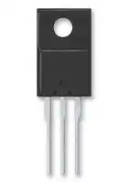
DGTD65T15H2TF
IGBT, 30 A, 1.65 V, 48 W, 650 V, ITO-220AB, 3 Pins
⚠️ Reference pricing provided. In case of supply shortages, we will connect you with our trusted procurement partners to ensure your project's continuity.
- Manufacturer: DIODES INC.
- Product type: Single IGBTs
- SVHC: Lead (25-Jun-2025)
- No. of Pins: 3Pins
- Product Range: -
- Power Dissipation: 48W
- Transistor Mounting: Through Hole
- Transistor Case Style: ITO-220AB
- Operating Temperature Max: 175°C
- Continuous Collector Current: 30A
- Collector Emitter Voltage Max: 650V
- Collector Emitter Saturation Voltage: 1.65V
| Delivery and price | |
|---|---|
| Units per pack | 500 |
| Price | 0.666 € |
| Current stock | 500+ |
| Lead time | 30 days |
Datasheet

**Green** ~~@,~~

**DGTD65T15H2TF** ~~[sd~~ **650V FIELD STOP IGBT IN ITO220AB**

## DIODES

## **Description**

The DGTD65T15H2TF is produced using advanced Field Stop Trench IGBT Technology, which provides high-performance, excellent quality, and high ruggedness.

## **Features**

- High Ruggedness for Motor Control

- VCE(sat) Positive Temperature Coefficient

- Very Soft, Fast Recovery Anti-Parallel Diode

- Low EMI

- Maximum Junction Temperature +175[°] C

- **Lead-Free Finish; RoHS Compliant (Notes 1 & 2)**

- **Halogen and Antimony Free. “Green” Device (Note 3)**

## **Applications**

- Motor Drive

## **Mechanical Data**

- Case: ITO220AB (Type MC)

- Case Material: Molded Plastic. “Green” Molding Compound. UL Flammability Classification Rating 94V-0

- Terminals: Finish—Matte Tin Plated Leads. Solderable per MIL-STD-202, Method 208

- Weight: 1.9 grams (Approximate)

G C E ITO220AB (Type MC)

**==> picture [92 x 111] intentionally omitted <==**

**----- Start of picture text -----**<br>
Collector<br>Gate<br>Emitter<br>Device Symbol<br>**----- End of picture text -----**<br>


## **Ordering Information** (Note 4)

|**Ordering Informationg Information Information** (Note 4)|||
|---|---|---|
|**Product**|**Marking**|**Quantity**|
|DGTD65T15H2TF|DGTD65T15H2|1000 per Box in Tubes (Note 5)|


Notes: 1. EU Directive 2002/95/EC (RoHS), 2011/65/EU (RoHS 2) & 2015/863/EU (RoHS 3).compliant. All applicable RoHS exemptions applied.

2. See https://www.diodes.com/quality/lead-free/ for more information about Diodes Incorporated’s definitions of Halogen- and Antimony-free, "Green" and Lead-free.

3. Halogen- and Antimony-free "Green” products are defined as those which contain <900ppm bromine, <900ppm chlorine (<1500ppm total Br + Cl) and <1000ppm antimony compounds.

4. For packaging details, go to our website at https://www.diodes.com/design/support/packaging/diodes-packaging/.

5. 50 devices per tube.

## **Marking Information**

**==> picture [45 x 23] intentionally omitted <==**

**----- Start of picture text -----**<br>
DGTD<br>65T15H2<br>YYLLLLLWW<br>**----- End of picture text -----**<br>


= Manufacturer’s Marking DGTD65T15H2 = Product Type Marking Code ain YY = Year (ex: 18 = 2018) LLLLL = Lot Code WW = Week (01 to 53)

1 of  9 **www.diodes.com**

DGTD65T15H2TF Document Number DS39649 Rev. 4 - 2

June 2018 © Diodes Incorporated

**DGTD65T15H2TF**

## **Absolute Maximum Ratings** (@TA = +25°C, unless otherwise specified.)

|**Absolute Maximum Ratingsgss** (@TA = +25°C, unless otherwise specified.)@TA = +25°C, unless otherwise specified.)A = +25°C, unless otherwise specified.)= +25°C, unless otherwise specified.)|**Absolute Maximum Ratingsgss** (@TA = +25°C, unless otherwise specified.)@TA = +25°C, unless otherwise specified.)A = +25°C, unless otherwise specified.)= +25°C, unless otherwise specified.)|(@TA = +25°C, unless otherwise specified.)@TA = +25°C, unless otherwise specified.)A = +25°C, unless otherwise specified.)= +25°C, unless otherwise specified.)pecified.)ecified.))|||
|---|---|---|---|---|
|**Characteristic**||**Symbol**|**Value**|**Unit**|
|Collector-Emitter Voltage||VCE|650|V|
|DC Collector Current, Limited by Tjmax|TC = +25°C|IC|30|A|
||TC = +100°C||15|A|
|Pulsed Collector Current,tp Limited byTjmax||ICpuls|60|A|
|Diode Forward Current Limited by Tjmax|TC = +25°C|IF|30|A|
||TC = +100°C||15|A|
|Diode Pulsed Current,tp Limited byTjmax||IFpuls|60|A|
|p<br>Gate-Emitter Voltage||VGE|±20|V|
|Short Circuit Withstand Time<br>VCC ≤360V,VGE = 15V, Tj = +150°C||tSC|5|µs|


## **Thermal Characteristics** (@TA = +25°C, unless otherwise specified.)

|**Thermal Characteristics** (@TA = +25°C, unless otherwise specified.)A = +25°C, unless otherwise specified.)= +25°C, unless otherwise specified.)|**Thermal Characteristics** (@TA = +25°C, unless otherwise specified.)A = +25°C, unless otherwise specified.)= +25°C, unless otherwise specified.)|(@TA = +25°C, unless otherwise specified.)A = +25°C, unless otherwise specified.)= +25°C, unless otherwise specified.)|||
|---|---|---|---|---|
|**Characteristic**||**Symbol**|**Value**|**Unit**|
|Power Dissipation Linear Derating Factor (Note 7)|TC = +25°C|PD|48|W|
||TC = +100°C||24||
|Thermal Resistance, Junction to Ambient (Note 6)||RϴJA|62|°C/W|
|Thermal Resistance, Junction to Case for IBGT (Note 7)||RϴJC|3.0||
|Thermal Resistance, Junction to Case for Diode (Note 7)||RϴJC|5.0||
|OperatingTemperature||Tj|-40 to +175|°C|
|Storage Temperature Range||TSTG|-55 to +150||


Note: 6. For a device mounted in a socket in still air conditions. Collector lead length 10mm.

7. For a device mounted on a Force Cooled Aluminium Heatsink 80x80x60mm.

2 of  9 **www.diodes.com**

DGTD65T15H2TF Document Number DS39649 Rev. 4 - 2

June 2018 © Diodes Incorporated

**DGTD65T15H2TF**

## **Thermal Characteristics and Derating Information**

**==> picture [493 x 407] intentionally omitted <==**

**----- Start of picture text -----**<br>
50 30<br>-— Power Dissipation for IGBT — Power Dissipation for Diode<br>PN 25<br>40<br>20<br>PT | CRN ee<br>30<br>PNEEEEE EL EAMW<br>15 HEE<br>COTTINET HH<br>20<br>10<br>TTT ST Pt tT NEEL<br>10<br>5<br>0 0<br>PFTLT ELEN~< =) Pp}~=6EEEEETTISXttt ING<br>0 20 40 60 80 100 120 140 160 180 0 20 40 60 80 100 120 140 160 180<br> Temperature (°C)  Temperature (°C)<br>Derating Curve Derating Curve<br>| 70 SELIILEEMALLUEA 35<br>30<br>S oof tara earben TTT Lp pt | | tt tt<br>©® so50 TUM TUM CMM CMC CMeV 25 Ne eee<br>° -HTMMECHE ECU Ce cg 20 Pot ING |<br>S 40 ST TT TTT TM ay lllll<br>15<br>& oo CaS SE TTT TTI pt | NE<br>10<br>5<br>E 10eA 0008 | Pt | tt INE EL<br>0<br>0 25 50 75 100 125 150 175 200<br>100u 1m 10m 100m 1 10 100° 1k<br>Pulse Width (s)  Case Temperature, TC (°C)<br>Transient Thermal Impedance Case Temperature-Collector Current<br> Max Power Dissipation (W)  Max Power Dissipation (W)<br> (A)<br>C<br>Collector Current, I<br>**----- End of picture text -----**<br>


3 of  9 **www.diodes.com**

DGTD65T15H2TF Document Number DS39649 Rev. 4 - 2

June 2018 © Diodes Incorporated

**DGTD65T15H2TF**

**Electrical Characteristics** (@Tj = +25°C, unless otherwise specified.)

|**Parameter**<br>**Symbol**<br>**Min**<br>**Typ**<br>**Max**<br>**Unit**<br>**Condition**<br>**STATIC CHARACTERISTICS**<br>Collector-Emitter Breakdown Voltage<br>BVCES<br>650<br>—<br>—<br>V<br>IC= 2mA,VGE= 0V<br>Collector-Emitter Saturation Voltage<br>Tj = +25°C<br>VCE(sat)<br>—<br>1.65<br>2.00<br>V<br>IC= 15A, VGE= 15V<br>Tj = +175°C<br>—<br>1.90<br>—<br>Diode Forward Voltage<br>Tj = +25°C<br>VF<br>—<br>1.85<br>2.30<br>V<br>VGE= 0V, IF= 15A<br>Tj = +175°C<br>—<br>1.95<br>—<br>Gate-Emitter Threshold Voltage<br>VGE(th)<br>4.5<br>5.5<br>6.5<br>V<br>VCE= VGE,IC= 0.5mA<br>Zero Gate Voltage Collector Current<br>ICES<br>—<br>—<br>20<br>µA<br>VCE= 650V, VGE= 0V,<br>Tj = +25°C<br>Gate-Emitter Leakage Current<br>IGES<br>—<br>—<br>±100<br>nA<br>VGE= 20V,VCE= 0V<br>**DYNAMIC CHARACTERISTICS**<br>Total Gate Charge<br>Qg<br>—<br>61<br>—<br>nC<br>VCE= 520V, IC= 15A,<br>VGE= 15V<br>Gate-Emitter Charge<br>Qge<br>—<br>11<br>—<br>Gate-Collector Charge<br>Qgc<br>—<br>35<br>—<br>Input Capacitance<br>Cies<br>—<br>1129<br>—<br>pF<br>VCE= 25V, VGE= 0V,<br>f = 1MHz<br>Reverse Transfer Capacitance<br>Cres<br>—<br>57<br>—<br>Output Capacitance<br>Coes<br>—<br>31<br>—<br>**SWITCHING CHARACTERISTICS**<br>Turn-On DelayTime<br>td(on)<br>—<br>19<br>—<br>ns<br>VGE= 15V, VCC= 400V,<br>IC= 15A, RG= 10Ω,<br>Inductive Load,<br>Tj= +25°C<br>Rise Time<br>tr<br>—<br>27<br>—<br>Turn-Off DelayTime<br>td(off)<br>—<br>128<br>—<br>Fall Time<br>tf<br>—<br>32<br>—<br>Turn-OnSwitchingEnergy<br>Eon<br>—<br>270<br>—<br>µJ<br>Turn-Off SwitchingEnergy<br>Eoff<br>—<br>86<br>—<br>TotalSwitchingEnergy<br>Ets<br>—<br>356<br>—<br>Turn-On DelayTime<br>td(on)<br>—<br>17<br>—<br>ns<br>VGE= 15V, VCC= 400V,<br>IC= 15A, RG= 10Ω,<br>Inductive Load,<br>Tj= +175°C<br>RiseTime<br>tr<br>—<br>29<br>—<br>Turn-Off DelayTime<br>td(off)<br>—<br>150<br>—<br>Fall Time<br>tf<br>—<br>130<br>—<br>Turn-On SwitchingEnergy<br>Eon<br>—<br>342<br>—<br>µJ<br>Turn-OffSwitchingEnergy<br>Eoff<br>—<br>288<br>—<br>Total SwitchingEnergy<br>Ets<br>—<br>630<br>—<br>ReverseRecoveryTime<br>trr<br>—<br>150<br>—<br>ns<br>IF= 15A, diF/dt = 200A/µs,<br>Tj= +25°C<br>Reverse RecoveryCurrent<br>Irr<br>—<br>5.2<br>—<br>A<br>ReverseRecovery Charge<br>Qrr<br>—<br>390<br>—<br>nC<br>Reverse RecoveryTime<br>trr<br>—<br>207<br>—<br>ns<br>IF= 15A, diF/dt = 200A/µs,<br>Tj= +175°C<br>ReverseRecovery Current<br>Irr<br>—<br>6.1<br>—<br>A<br>ReverseRecovery Charge<br>Qrr<br>—<br>631<br>—<br>nC<br>~~Pe~~<br>~~ff~~<br>~~—__$~~<br>~~<_<~~<br>~~es~~<br>~~ee~~<br>~~nD~~<br>~~DO~~<br>~~GO~~<br>~~—_}~~<br>~~ff}~~<br>~~}~~<br>~~Ce~~<br>~~ff~~<br>~~I~~<br>~~a~~<br>~~es~~<br>~~I~~<br>~~I~~<br>~~sD~~<br>~~os~~<br>~~ee~~<br>~~SSS~~<br>~~sD~~<br>~~ee~~<br>~~a~~<br>~~ee~~<br>~~**e**e~~<br>~~y~~<br>~~(I~~<br>~~I RDI~~|**Parameter**<br>**Symbol**<br>**Min**<br>**Typ**<br>**Max**<br>**Unit**<br>**Condition**<br>**STATIC CHARACTERISTICS**<br>Collector-Emitter Breakdown Voltage<br>BVCES<br>650<br>—<br>—<br>V<br>IC= 2mA,VGE= 0V<br>Collector-Emitter Saturation Voltage<br>Tj = +25°C<br>VCE(sat)<br>—<br>1.65<br>2.00<br>V<br>IC= 15A, VGE= 15V<br>Tj = +175°C<br>—<br>1.90<br>—<br>Diode Forward Voltage<br>Tj = +25°C<br>VF<br>—<br>1.85<br>2.30<br>V<br>VGE= 0V, IF= 15A<br>Tj = +175°C<br>—<br>1.95<br>—<br>Gate-Emitter Threshold Voltage<br>VGE(th)<br>4.5<br>5.5<br>6.5<br>V<br>VCE= VGE,IC= 0.5mA<br>Zero Gate Voltage Collector Current<br>ICES<br>—<br>—<br>20<br>µA<br>VCE= 650V, VGE= 0V,<br>Tj = +25°C<br>Gate-Emitter Leakage Current<br>IGES<br>—<br>—<br>±100<br>nA<br>VGE= 20V,VCE= 0V<br>**DYNAMIC CHARACTERISTICS**<br>Total Gate Charge<br>Qg<br>—<br>61<br>—<br>nC<br>VCE= 520V, IC= 15A,<br>VGE= 15V<br>Gate-Emitter Charge<br>Qge<br>—<br>11<br>—<br>Gate-Collector Charge<br>Qgc<br>—<br>35<br>—<br>Input Capacitance<br>Cies<br>—<br>1129<br>—<br>pF<br>VCE= 25V, VGE= 0V,<br>f = 1MHz<br>Reverse Transfer Capacitance<br>Cres<br>—<br>57<br>—<br>Output Capacitance<br>Coes<br>—<br>31<br>—<br>**SWITCHING CHARACTERISTICS**<br>Turn-On DelayTime<br>td(on)<br>—<br>19<br>—<br>ns<br>VGE= 15V, VCC= 400V,<br>IC= 15A, RG= 10Ω,<br>Inductive Load,<br>Tj= +25°C<br>Rise Time<br>tr<br>—<br>27<br>—<br>Turn-Off DelayTime<br>td(off)<br>—<br>128<br>—<br>Fall Time<br>tf<br>—<br>32<br>—<br>Turn-OnSwitchingEnergy<br>Eon<br>—<br>270<br>—<br>µJ<br>Turn-Off SwitchingEnergy<br>Eoff<br>—<br>86<br>—<br>TotalSwitchingEnergy<br>Ets<br>—<br>356<br>—<br>Turn-On DelayTime<br>td(on)<br>—<br>17<br>—<br>ns<br>VGE= 15V, VCC= 400V,<br>IC= 15A, RG= 10Ω,<br>Inductive Load,<br>Tj= +175°C<br>RiseTime<br>tr<br>—<br>29<br>—<br>Turn-Off DelayTime<br>td(off)<br>—<br>150<br>—<br>Fall Time<br>tf<br>—<br>130<br>—<br>Turn-On SwitchingEnergy<br>Eon<br>—<br>342<br>—<br>µJ<br>Turn-OffSwitchingEnergy<br>Eoff<br>—<br>288<br>—<br>Total SwitchingEnergy<br>Ets<br>—<br>630<br>—<br>ReverseRecoveryTime<br>trr<br>—<br>150<br>—<br>ns<br>IF= 15A, diF/dt = 200A/µs,<br>Tj= +25°C<br>Reverse RecoveryCurrent<br>Irr<br>—<br>5.2<br>—<br>A<br>ReverseRecovery Charge<br>Qrr<br>—<br>390<br>—<br>nC<br>Reverse RecoveryTime<br>trr<br>—<br>207<br>—<br>ns<br>IF= 15A, diF/dt = 200A/µs,<br>Tj= +175°C<br>ReverseRecovery Current<br>Irr<br>—<br>6.1<br>—<br>A<br>ReverseRecovery Charge<br>Qrr<br>—<br>631<br>—<br>nC<br>~~Pe~~<br>~~ff~~<br>~~—__$~~<br>~~<_<~~<br>~~es~~<br>~~ee~~<br>~~nD~~<br>~~DO~~<br>~~GO~~<br>~~—_}~~<br>~~ff}~~<br>~~}~~<br>~~Ce~~<br>~~ff~~<br>~~I~~<br>~~a~~<br>~~es~~<br>~~I~~<br>~~I~~<br>~~sD~~<br>~~os~~<br>~~ee~~<br>~~SSS~~<br>~~sD~~<br>~~ee~~<br>~~a~~<br>~~ee~~<br>~~**e**e~~<br>~~y~~<br>~~(I~~<br>~~I RDI~~|**Parameter**<br>**Symbol**<br>**Min**<br>**Typ**<br>**Max**<br>**Unit**<br>**Condition**<br>**STATIC CHARACTERISTICS**<br>Collector-Emitter Breakdown Voltage<br>BVCES<br>650<br>—<br>—<br>V<br>IC= 2mA,VGE= 0V<br>Collector-Emitter Saturation Voltage<br>Tj = +25°C<br>VCE(sat)<br>—<br>1.65<br>2.00<br>V<br>IC= 15A, VGE= 15V<br>Tj = +175°C<br>—<br>1.90<br>—<br>Diode Forward Voltage<br>Tj = +25°C<br>VF<br>—<br>1.85<br>2.30<br>V<br>VGE= 0V, IF= 15A<br>Tj = +175°C<br>—<br>1.95<br>—<br>Gate-Emitter Threshold Voltage<br>VGE(th)<br>4.5<br>5.5<br>6.5<br>V<br>VCE= VGE,IC= 0.5mA<br>Zero Gate Voltage Collector Current<br>ICES<br>—<br>—<br>20<br>µA<br>VCE= 650V, VGE= 0V,<br>Tj = +25°C<br>Gate-Emitter Leakage Current<br>IGES<br>—<br>—<br>±100<br>nA<br>VGE= 20V,VCE= 0V<br>**DYNAMIC CHARACTERISTICS**<br>Total Gate Charge<br>Qg<br>—<br>61<br>—<br>nC<br>VCE= 520V, IC= 15A,<br>VGE= 15V<br>Gate-Emitter Charge<br>Qge<br>—<br>11<br>—<br>Gate-Collector Charge<br>Qgc<br>—<br>35<br>—<br>Input Capacitance<br>Cies<br>—<br>1129<br>—<br>pF<br>VCE= 25V, VGE= 0V,<br>f = 1MHz<br>Reverse Transfer Capacitance<br>Cres<br>—<br>57<br>—<br>Output Capacitance<br>Coes<br>—<br>31<br>—<br>**SWITCHING CHARACTERISTICS**<br>Turn-On DelayTime<br>td(on)<br>—<br>19<br>—<br>ns<br>VGE= 15V, VCC= 400V,<br>IC= 15A, RG= 10Ω,<br>Inductive Load,<br>Tj= +25°C<br>Rise Time<br>tr<br>—<br>27<br>—<br>Turn-Off DelayTime<br>td(off)<br>—<br>128<br>—<br>Fall Time<br>tf<br>—<br>32<br>—<br>Turn-OnSwitchingEnergy<br>Eon<br>—<br>270<br>—<br>µJ<br>Turn-Off SwitchingEnergy<br>Eoff<br>—<br>86<br>—<br>TotalSwitchingEnergy<br>Ets<br>—<br>356<br>—<br>Turn-On DelayTime<br>td(on)<br>—<br>17<br>—<br>ns<br>VGE= 15V, VCC= 400V,<br>IC= 15A, RG= 10Ω,<br>Inductive Load,<br>Tj= +175°C<br>RiseTime<br>tr<br>—<br>29<br>—<br>Turn-Off DelayTime<br>td(off)<br>—<br>150<br>—<br>Fall Time<br>tf<br>—<br>130<br>—<br>Turn-On SwitchingEnergy<br>Eon<br>—<br>342<br>—<br>µJ<br>Turn-OffSwitchingEnergy<br>Eoff<br>—<br>288<br>—<br>Total SwitchingEnergy<br>Ets<br>—<br>630<br>—<br>ReverseRecoveryTime<br>trr<br>—<br>150<br>—<br>ns<br>IF= 15A, diF/dt = 200A/µs,<br>Tj= +25°C<br>Reverse RecoveryCurrent<br>Irr<br>—<br>5.2<br>—<br>A<br>ReverseRecovery Charge<br>Qrr<br>—<br>390<br>—<br>nC<br>Reverse RecoveryTime<br>trr<br>—<br>207<br>—<br>ns<br>IF= 15A, diF/dt = 200A/µs,<br>Tj= +175°C<br>ReverseRecovery Current<br>Irr<br>—<br>6.1<br>—<br>A<br>ReverseRecovery Charge<br>Qrr<br>—<br>631<br>—<br>nC<br>~~Pe~~<br>~~ff~~<br>~~—__$~~<br>~~<_<~~<br>~~es~~<br>~~ee~~<br>~~nD~~<br>~~DO~~<br>~~GO~~<br>~~—_}~~<br>~~ff}~~<br>~~}~~<br>~~Ce~~<br>~~ff~~<br>~~I~~<br>~~a~~<br>~~es~~<br>~~I~~<br>~~I~~<br>~~sD~~<br>~~os~~<br>~~ee~~<br>~~SSS~~<br>~~sD~~<br>~~ee~~<br>~~a~~<br>~~ee~~<br>~~**e**e~~<br>~~y~~<br>~~(I~~<br>~~I RDI~~|**Parameter**<br>**Symbol**<br>**Min**<br>**Typ**<br>**Max**<br>**Unit**<br>**Condition**<br>**STATIC CHARACTERISTICS**<br>Collector-Emitter Breakdown Voltage<br>BVCES<br>650<br>—<br>—<br>V<br>IC= 2mA,VGE= 0V<br>Collector-Emitter Saturation Voltage<br>Tj = +25°C<br>VCE(sat)<br>—<br>1.65<br>2.00<br>V<br>IC= 15A, VGE= 15V<br>Tj = +175°C<br>—<br>1.90<br>—<br>Diode Forward Voltage<br>Tj = +25°C<br>VF<br>—<br>1.85<br>2.30<br>V<br>VGE= 0V, IF= 15A<br>Tj = +175°C<br>—<br>1.95<br>—<br>Gate-Emitter Threshold Voltage<br>VGE(th)<br>4.5<br>5.5<br>6.5<br>V<br>VCE= VGE,IC= 0.5mA<br>Zero Gate Voltage Collector Current<br>ICES<br>—<br>—<br>20<br>µA<br>VCE= 650V, VGE= 0V,<br>Tj = +25°C<br>Gate-Emitter Leakage Current<br>IGES<br>—<br>—<br>±100<br>nA<br>VGE= 20V,VCE= 0V<br>**DYNAMIC CHARACTERISTICS**<br>Total Gate Charge<br>Qg<br>—<br>61<br>—<br>nC<br>VCE= 520V, IC= 15A,<br>VGE= 15V<br>Gate-Emitter Charge<br>Qge<br>—<br>11<br>—<br>Gate-Collector Charge<br>Qgc<br>—<br>35<br>—<br>Input Capacitance<br>Cies<br>—<br>1129<br>—<br>pF<br>VCE= 25V, VGE= 0V,<br>f = 1MHz<br>Reverse Transfer Capacitance<br>Cres<br>—<br>57<br>—<br>Output Capacitance<br>Coes<br>—<br>31<br>—<br>**SWITCHING CHARACTERISTICS**<br>Turn-On DelayTime<br>td(on)<br>—<br>19<br>—<br>ns<br>VGE= 15V, VCC= 400V,<br>IC= 15A, RG= 10Ω,<br>Inductive Load,<br>Tj= +25°C<br>Rise Time<br>tr<br>—<br>27<br>—<br>Turn-Off DelayTime<br>td(off)<br>—<br>128<br>—<br>Fall Time<br>tf<br>—<br>32<br>—<br>Turn-OnSwitchingEnergy<br>Eon<br>—<br>270<br>—<br>µJ<br>Turn-Off SwitchingEnergy<br>Eoff<br>—<br>86<br>—<br>TotalSwitchingEnergy<br>Ets<br>—<br>356<br>—<br>Turn-On DelayTime<br>td(on)<br>—<br>17<br>—<br>ns<br>VGE= 15V, VCC= 400V,<br>IC= 15A, RG= 10Ω,<br>Inductive Load,<br>Tj= +175°C<br>RiseTime<br>tr<br>—<br>29<br>—<br>Turn-Off DelayTime<br>td(off)<br>—<br>150<br>—<br>Fall Time<br>tf<br>—<br>130<br>—<br>Turn-On SwitchingEnergy<br>Eon<br>—<br>342<br>—<br>µJ<br>Turn-OffSwitchingEnergy<br>Eoff<br>—<br>288<br>—<br>Total SwitchingEnergy<br>Ets<br>—<br>630<br>—<br>ReverseRecoveryTime<br>trr<br>—<br>150<br>—<br>ns<br>IF= 15A, diF/dt = 200A/µs,<br>Tj= +25°C<br>Reverse RecoveryCurrent<br>Irr<br>—<br>5.2<br>—<br>A<br>ReverseRecovery Charge<br>Qrr<br>—<br>390<br>—<br>nC<br>Reverse RecoveryTime<br>trr<br>—<br>207<br>—<br>ns<br>IF= 15A, diF/dt = 200A/µs,<br>Tj= +175°C<br>ReverseRecovery Current<br>Irr<br>—<br>6.1<br>—<br>A<br>ReverseRecovery Charge<br>Qrr<br>—<br>631<br>—<br>nC<br>~~Pe~~<br>~~ff~~<br>~~—__$~~<br>~~<_<~~<br>~~es~~<br>~~ee~~<br>~~nD~~<br>~~DO~~<br>~~GO~~<br>~~—_}~~<br>~~ff}~~<br>~~}~~<br>~~Ce~~<br>~~ff~~<br>~~I~~<br>~~a~~<br>~~es~~<br>~~I~~<br>~~I~~<br>~~sD~~<br>~~os~~<br>~~ee~~<br>~~SSS~~<br>~~sD~~<br>~~ee~~<br>~~a~~<br>~~ee~~<br>~~**e**e~~<br>~~y~~<br>~~(I~~<br>~~I RDI~~|**Parameter**<br>**Symbol**<br>**Min**<br>**Typ**<br>**Max**<br>**Unit**<br>**Condition**<br>**STATIC CHARACTERISTICS**<br>Collector-Emitter Breakdown Voltage<br>BVCES<br>650<br>—<br>—<br>V<br>IC= 2mA,VGE= 0V<br>Collector-Emitter Saturation Voltage<br>Tj = +25°C<br>VCE(sat)<br>—<br>1.65<br>2.00<br>V<br>IC= 15A, VGE= 15V<br>Tj = +175°C<br>—<br>1.90<br>—<br>Diode Forward Voltage<br>Tj = +25°C<br>VF<br>—<br>1.85<br>2.30<br>V<br>VGE= 0V, IF= 15A<br>Tj = +175°C<br>—<br>1.95<br>—<br>Gate-Emitter Threshold Voltage<br>VGE(th)<br>4.5<br>5.5<br>6.5<br>V<br>VCE= VGE,IC= 0.5mA<br>Zero Gate Voltage Collector Current<br>ICES<br>—<br>—<br>20<br>µA<br>VCE= 650V, VGE= 0V,<br>Tj = +25°C<br>Gate-Emitter Leakage Current<br>IGES<br>—<br>—<br>±100<br>nA<br>VGE= 20V,VCE= 0V<br>**DYNAMIC CHARACTERISTICS**<br>Total Gate Charge<br>Qg<br>—<br>61<br>—<br>nC<br>VCE= 520V, IC= 15A,<br>VGE= 15V<br>Gate-Emitter Charge<br>Qge<br>—<br>11<br>—<br>Gate-Collector Charge<br>Qgc<br>—<br>35<br>—<br>Input Capacitance<br>Cies<br>—<br>1129<br>—<br>pF<br>VCE= 25V, VGE= 0V,<br>f = 1MHz<br>Reverse Transfer Capacitance<br>Cres<br>—<br>57<br>—<br>Output Capacitance<br>Coes<br>—<br>31<br>—<br>**SWITCHING CHARACTERISTICS**<br>Turn-On DelayTime<br>td(on)<br>—<br>19<br>—<br>ns<br>VGE= 15V, VCC= 400V,<br>IC= 15A, RG= 10Ω,<br>Inductive Load,<br>Tj= +25°C<br>Rise Time<br>tr<br>—<br>27<br>—<br>Turn-Off DelayTime<br>td(off)<br>—<br>128<br>—<br>Fall Time<br>tf<br>—<br>32<br>—<br>Turn-OnSwitchingEnergy<br>Eon<br>—<br>270<br>—<br>µJ<br>Turn-Off SwitchingEnergy<br>Eoff<br>—<br>86<br>—<br>TotalSwitchingEnergy<br>Ets<br>—<br>356<br>—<br>Turn-On DelayTime<br>td(on)<br>—<br>17<br>—<br>ns<br>VGE= 15V, VCC= 400V,<br>IC= 15A, RG= 10Ω,<br>Inductive Load,<br>Tj= +175°C<br>RiseTime<br>tr<br>—<br>29<br>—<br>Turn-Off DelayTime<br>td(off)<br>—<br>150<br>—<br>Fall Time<br>tf<br>—<br>130<br>—<br>Turn-On SwitchingEnergy<br>Eon<br>—<br>342<br>—<br>µJ<br>Turn-OffSwitchingEnergy<br>Eoff<br>—<br>288<br>—<br>Total SwitchingEnergy<br>Ets<br>—<br>630<br>—<br>ReverseRecoveryTime<br>trr<br>—<br>150<br>—<br>ns<br>IF= 15A, diF/dt = 200A/µs,<br>Tj= +25°C<br>Reverse RecoveryCurrent<br>Irr<br>—<br>5.2<br>—<br>A<br>ReverseRecovery Charge<br>Qrr<br>—<br>390<br>—<br>nC<br>Reverse RecoveryTime<br>trr<br>—<br>207<br>—<br>ns<br>IF= 15A, diF/dt = 200A/µs,<br>Tj= +175°C<br>ReverseRecovery Current<br>Irr<br>—<br>6.1<br>—<br>A<br>ReverseRecovery Charge<br>Qrr<br>—<br>631<br>—<br>nC<br>~~Pe~~<br>~~ff~~<br>~~—__$~~<br>~~<_<~~<br>~~es~~<br>~~ee~~<br>~~nD~~<br>~~DO~~<br>~~GO~~<br>~~—_}~~<br>~~ff}~~<br>~~}~~<br>~~Ce~~<br>~~ff~~<br>~~I~~<br>~~a~~<br>~~es~~<br>~~I~~<br>~~I~~<br>~~sD~~<br>~~os~~<br>~~ee~~<br>~~SSS~~<br>~~sD~~<br>~~ee~~<br>~~a~~<br>~~ee~~<br>~~**e**e~~<br>~~y~~<br>~~(I~~<br>~~I RDI~~|**Parameter**<br>**Symbol**<br>**Min**<br>**Typ**<br>**Max**<br>**Unit**<br>**Condition**<br>**STATIC CHARACTERISTICS**<br>Collector-Emitter Breakdown Voltage<br>BVCES<br>650<br>—<br>—<br>V<br>IC= 2mA,VGE= 0V<br>Collector-Emitter Saturation Voltage<br>Tj = +25°C<br>VCE(sat)<br>—<br>1.65<br>2.00<br>V<br>IC= 15A, VGE= 15V<br>Tj = +175°C<br>—<br>1.90<br>—<br>Diode Forward Voltage<br>Tj = +25°C<br>VF<br>—<br>1.85<br>2.30<br>V<br>VGE= 0V, IF= 15A<br>Tj = +175°C<br>—<br>1.95<br>—<br>Gate-Emitter Threshold Voltage<br>VGE(th)<br>4.5<br>5.5<br>6.5<br>V<br>VCE= VGE,IC= 0.5mA<br>Zero Gate Voltage Collector Current<br>ICES<br>—<br>—<br>20<br>µA<br>VCE= 650V, VGE= 0V,<br>Tj = +25°C<br>Gate-Emitter Leakage Current<br>IGES<br>—<br>—<br>±100<br>nA<br>VGE= 20V,VCE= 0V<br>**DYNAMIC CHARACTERISTICS**<br>Total Gate Charge<br>Qg<br>—<br>61<br>—<br>nC<br>VCE= 520V, IC= 15A,<br>VGE= 15V<br>Gate-Emitter Charge<br>Qge<br>—<br>11<br>—<br>Gate-Collector Charge<br>Qgc<br>—<br>35<br>—<br>Input Capacitance<br>Cies<br>—<br>1129<br>—<br>pF<br>VCE= 25V, VGE= 0V,<br>f = 1MHz<br>Reverse Transfer Capacitance<br>Cres<br>—<br>57<br>—<br>Output Capacitance<br>Coes<br>—<br>31<br>—<br>**SWITCHING CHARACTERISTICS**<br>Turn-On DelayTime<br>td(on)<br>—<br>19<br>—<br>ns<br>VGE= 15V, VCC= 400V,<br>IC= 15A, RG= 10Ω,<br>Inductive Load,<br>Tj= +25°C<br>Rise Time<br>tr<br>—<br>27<br>—<br>Turn-Off DelayTime<br>td(off)<br>—<br>128<br>—<br>Fall Time<br>tf<br>—<br>32<br>—<br>Turn-OnSwitchingEnergy<br>Eon<br>—<br>270<br>—<br>µJ<br>Turn-Off SwitchingEnergy<br>Eoff<br>—<br>86<br>—<br>TotalSwitchingEnergy<br>Ets<br>—<br>356<br>—<br>Turn-On DelayTime<br>td(on)<br>—<br>17<br>—<br>ns<br>VGE= 15V, VCC= 400V,<br>IC= 15A, RG= 10Ω,<br>Inductive Load,<br>Tj= +175°C<br>RiseTime<br>tr<br>—<br>29<br>—<br>Turn-Off DelayTime<br>td(off)<br>—<br>150<br>—<br>Fall Time<br>tf<br>—<br>130<br>—<br>Turn-On SwitchingEnergy<br>Eon<br>—<br>342<br>—<br>µJ<br>Turn-OffSwitchingEnergy<br>Eoff<br>—<br>288<br>—<br>Total SwitchingEnergy<br>Ets<br>—<br>630<br>—<br>ReverseRecoveryTime<br>trr<br>—<br>150<br>—<br>ns<br>IF= 15A, diF/dt = 200A/µs,<br>Tj= +25°C<br>Reverse RecoveryCurrent<br>Irr<br>—<br>5.2<br>—<br>A<br>ReverseRecovery Charge<br>Qrr<br>—<br>390<br>—<br>nC<br>Reverse RecoveryTime<br>trr<br>—<br>207<br>—<br>ns<br>IF= 15A, diF/dt = 200A/µs,<br>Tj= +175°C<br>ReverseRecovery Current<br>Irr<br>—<br>6.1<br>—<br>A<br>ReverseRecovery Charge<br>Qrr<br>—<br>631<br>—<br>nC<br>~~Pe~~<br>~~ff~~<br>~~—__$~~<br>~~<_<~~<br>~~es~~<br>~~ee~~<br>~~nD~~<br>~~DO~~<br>~~GO~~<br>~~—_}~~<br>~~ff}~~<br>~~}~~<br>~~Ce~~<br>~~ff~~<br>~~I~~<br>~~a~~<br>~~es~~<br>~~I~~<br>~~I~~<br>~~sD~~<br>~~os~~<br>~~ee~~<br>~~SSS~~<br>~~sD~~<br>~~ee~~<br>~~a~~<br>~~ee~~<br>~~**e**e~~<br>~~y~~<br>~~(I~~<br>~~I RDI~~|**Parameter**<br>**Symbol**<br>**Min**<br>**Typ**<br>**Max**<br>**Unit**<br>**Condition**<br>**STATIC CHARACTERISTICS**<br>Collector-Emitter Breakdown Voltage<br>BVCES<br>650<br>—<br>—<br>V<br>IC= 2mA,VGE= 0V<br>Collector-Emitter Saturation Voltage<br>Tj = +25°C<br>VCE(sat)<br>—<br>1.65<br>2.00<br>V<br>IC= 15A, VGE= 15V<br>Tj = +175°C<br>—<br>1.90<br>—<br>Diode Forward Voltage<br>Tj = +25°C<br>VF<br>—<br>1.85<br>2.30<br>V<br>VGE= 0V, IF= 15A<br>Tj = +175°C<br>—<br>1.95<br>—<br>Gate-Emitter Threshold Voltage<br>VGE(th)<br>4.5<br>5.5<br>6.5<br>V<br>VCE= VGE,IC= 0.5mA<br>Zero Gate Voltage Collector Current<br>ICES<br>—<br>—<br>20<br>µA<br>VCE= 650V, VGE= 0V,<br>Tj = +25°C<br>Gate-Emitter Leakage Current<br>IGES<br>—<br>—<br>±100<br>nA<br>VGE= 20V,VCE= 0V<br>**DYNAMIC CHARACTERISTICS**<br>Total Gate Charge<br>Qg<br>—<br>61<br>—<br>nC<br>VCE= 520V, IC= 15A,<br>VGE= 15V<br>Gate-Emitter Charge<br>Qge<br>—<br>11<br>—<br>Gate-Collector Charge<br>Qgc<br>—<br>35<br>—<br>Input Capacitance<br>Cies<br>—<br>1129<br>—<br>pF<br>VCE= 25V, VGE= 0V,<br>f = 1MHz<br>Reverse Transfer Capacitance<br>Cres<br>—<br>57<br>—<br>Output Capacitance<br>Coes<br>—<br>31<br>—<br>**SWITCHING CHARACTERISTICS**<br>Turn-On DelayTime<br>td(on)<br>—<br>19<br>—<br>ns<br>VGE= 15V, VCC= 400V,<br>IC= 15A, RG= 10Ω,<br>Inductive Load,<br>Tj= +25°C<br>Rise Time<br>tr<br>—<br>27<br>—<br>Turn-Off DelayTime<br>td(off)<br>—<br>128<br>—<br>Fall Time<br>tf<br>—<br>32<br>—<br>Turn-OnSwitchingEnergy<br>Eon<br>—<br>270<br>—<br>µJ<br>Turn-Off SwitchingEnergy<br>Eoff<br>—<br>86<br>—<br>TotalSwitchingEnergy<br>Ets<br>—<br>356<br>—<br>Turn-On DelayTime<br>td(on)<br>—<br>17<br>—<br>ns<br>VGE= 15V, VCC= 400V,<br>IC= 15A, RG= 10Ω,<br>Inductive Load,<br>Tj= +175°C<br>RiseTime<br>tr<br>—<br>29<br>—<br>Turn-Off DelayTime<br>td(off)<br>—<br>150<br>—<br>Fall Time<br>tf<br>—<br>130<br>—<br>Turn-On SwitchingEnergy<br>Eon<br>—<br>342<br>—<br>µJ<br>Turn-OffSwitchingEnergy<br>Eoff<br>—<br>288<br>—<br>Total SwitchingEnergy<br>Ets<br>—<br>630<br>—<br>ReverseRecoveryTime<br>trr<br>—<br>150<br>—<br>ns<br>IF= 15A, diF/dt = 200A/µs,<br>Tj= +25°C<br>Reverse RecoveryCurrent<br>Irr<br>—<br>5.2<br>—<br>A<br>ReverseRecovery Charge<br>Qrr<br>—<br>390<br>—<br>nC<br>Reverse RecoveryTime<br>trr<br>—<br>207<br>—<br>ns<br>IF= 15A, diF/dt = 200A/µs,<br>Tj= +175°C<br>ReverseRecovery Current<br>Irr<br>—<br>6.1<br>—<br>A<br>ReverseRecovery Charge<br>Qrr<br>—<br>631<br>—<br>nC<br>~~Pe~~<br>~~ff~~<br>~~—__$~~<br>~~<_<~~<br>~~es~~<br>~~ee~~<br>~~nD~~<br>~~DO~~<br>~~GO~~<br>~~—_}~~<br>~~ff}~~<br>~~}~~<br>~~Ce~~<br>~~ff~~<br>~~I~~<br>~~a~~<br>~~es~~<br>~~I~~<br>~~I~~<br>~~sD~~<br>~~os~~<br>~~ee~~<br>~~SSS~~<br>~~sD~~<br>~~ee~~<br>~~a~~<br>~~ee~~<br>~~**e**e~~<br>~~y~~<br>~~(I~~<br>~~I RDI~~|**Parameter**<br>**Symbol**<br>**Min**<br>**Typ**<br>**Max**<br>**Unit**<br>**Condition**<br>**STATIC CHARACTERISTICS**<br>Collector-Emitter Breakdown Voltage<br>BVCES<br>650<br>—<br>—<br>V<br>IC= 2mA,VGE= 0V<br>Collector-Emitter Saturation Voltage<br>Tj = +25°C<br>VCE(sat)<br>—<br>1.65<br>2.00<br>V<br>IC= 15A, VGE= 15V<br>Tj = +175°C<br>—<br>1.90<br>—<br>Diode Forward Voltage<br>Tj = +25°C<br>VF<br>—<br>1.85<br>2.30<br>V<br>VGE= 0V, IF= 15A<br>Tj = +175°C<br>—<br>1.95<br>—<br>Gate-Emitter Threshold Voltage<br>VGE(th)<br>4.5<br>5.5<br>6.5<br>V<br>VCE= VGE,IC= 0.5mA<br>Zero Gate Voltage Collector Current<br>ICES<br>—<br>—<br>20<br>µA<br>VCE= 650V, VGE= 0V,<br>Tj = +25°C<br>Gate-Emitter Leakage Current<br>IGES<br>—<br>—<br>±100<br>nA<br>VGE= 20V,VCE= 0V<br>**DYNAMIC CHARACTERISTICS**<br>Total Gate Charge<br>Qg<br>—<br>61<br>—<br>nC<br>VCE= 520V, IC= 15A,<br>VGE= 15V<br>Gate-Emitter Charge<br>Qge<br>—<br>11<br>—<br>Gate-Collector Charge<br>Qgc<br>—<br>35<br>—<br>Input Capacitance<br>Cies<br>—<br>1129<br>—<br>pF<br>VCE= 25V, VGE= 0V,<br>f = 1MHz<br>Reverse Transfer Capacitance<br>Cres<br>—<br>57<br>—<br>Output Capacitance<br>Coes<br>—<br>31<br>—<br>**SWITCHING CHARACTERISTICS**<br>Turn-On DelayTime<br>td(on)<br>—<br>19<br>—<br>ns<br>VGE= 15V, VCC= 400V,<br>IC= 15A, RG= 10Ω,<br>Inductive Load,<br>Tj= +25°C<br>Rise Time<br>tr<br>—<br>27<br>—<br>Turn-Off DelayTime<br>td(off)<br>—<br>128<br>—<br>Fall Time<br>tf<br>—<br>32<br>—<br>Turn-OnSwitchingEnergy<br>Eon<br>—<br>270<br>—<br>µJ<br>Turn-Off SwitchingEnergy<br>Eoff<br>—<br>86<br>—<br>TotalSwitchingEnergy<br>Ets<br>—<br>356<br>—<br>Turn-On DelayTime<br>td(on)<br>—<br>17<br>—<br>ns<br>VGE= 15V, VCC= 400V,<br>IC= 15A, RG= 10Ω,<br>Inductive Load,<br>Tj= +175°C<br>RiseTime<br>tr<br>—<br>29<br>—<br>Turn-Off DelayTime<br>td(off)<br>—<br>150<br>—<br>Fall Time<br>tf<br>—<br>130<br>—<br>Turn-On SwitchingEnergy<br>Eon<br>—<br>342<br>—<br>µJ<br>Turn-OffSwitchingEnergy<br>Eoff<br>—<br>288<br>—<br>Total SwitchingEnergy<br>Ets<br>—<br>630<br>—<br>ReverseRecoveryTime<br>trr<br>—<br>150<br>—<br>ns<br>IF= 15A, diF/dt = 200A/µs,<br>Tj= +25°C<br>Reverse RecoveryCurrent<br>Irr<br>—<br>5.2<br>—<br>A<br>ReverseRecovery Charge<br>Qrr<br>—<br>390<br>—<br>nC<br>Reverse RecoveryTime<br>trr<br>—<br>207<br>—<br>ns<br>IF= 15A, diF/dt = 200A/µs,<br>Tj= +175°C<br>ReverseRecovery Current<br>Irr<br>—<br>6.1<br>—<br>A<br>ReverseRecovery Charge<br>Qrr<br>—<br>631<br>—<br>nC<br>~~Pe~~<br>~~ff~~<br>~~—__$~~<br>~~<_<~~<br>~~es~~<br>~~ee~~<br>~~nD~~<br>~~DO~~<br>~~GO~~<br>~~—_}~~<br>~~ff}~~<br>~~}~~<br>~~Ce~~<br>~~ff~~<br>~~I~~<br>~~a~~<br>~~es~~<br>~~I~~<br>~~I~~<br>~~sD~~<br>~~os~~<br>~~ee~~<br>~~SSS~~<br>~~sD~~<br>~~ee~~<br>~~a~~<br>~~ee~~<br>~~**e**e~~<br>~~y~~<br>~~(I~~<br>~~I RDI~~|**Parameter**<br>**Symbol**<br>**Min**<br>**Typ**<br>**Max**<br>**Unit**<br>**Condition**<br>**STATIC CHARACTERISTICS**<br>Collector-Emitter Breakdown Voltage<br>BVCES<br>650<br>—<br>—<br>V<br>IC= 2mA,VGE= 0V<br>Collector-Emitter Saturation Voltage<br>Tj = +25°C<br>VCE(sat)<br>—<br>1.65<br>2.00<br>V<br>IC= 15A, VGE= 15V<br>Tj = +175°C<br>—<br>1.90<br>—<br>Diode Forward Voltage<br>Tj = +25°C<br>VF<br>—<br>1.85<br>2.30<br>V<br>VGE= 0V, IF= 15A<br>Tj = +175°C<br>—<br>1.95<br>—<br>Gate-Emitter Threshold Voltage<br>VGE(th)<br>4.5<br>5.5<br>6.5<br>V<br>VCE= VGE,IC= 0.5mA<br>Zero Gate Voltage Collector Current<br>ICES<br>—<br>—<br>20<br>µA<br>VCE= 650V, VGE= 0V,<br>Tj = +25°C<br>Gate-Emitter Leakage Current<br>IGES<br>—<br>—<br>±100<br>nA<br>VGE= 20V,VCE= 0V<br>**DYNAMIC CHARACTERISTICS**<br>Total Gate Charge<br>Qg<br>—<br>61<br>—<br>nC<br>VCE= 520V, IC= 15A,<br>VGE= 15V<br>Gate-Emitter Charge<br>Qge<br>—<br>11<br>—<br>Gate-Collector Charge<br>Qgc<br>—<br>35<br>—<br>Input Capacitance<br>Cies<br>—<br>1129<br>—<br>pF<br>VCE= 25V, VGE= 0V,<br>f = 1MHz<br>Reverse Transfer Capacitance<br>Cres<br>—<br>57<br>—<br>Output Capacitance<br>Coes<br>—<br>31<br>—<br>**SWITCHING CHARACTERISTICS**<br>Turn-On DelayTime<br>td(on)<br>—<br>19<br>—<br>ns<br>VGE= 15V, VCC= 400V,<br>IC= 15A, RG= 10Ω,<br>Inductive Load,<br>Tj= +25°C<br>Rise Time<br>tr<br>—<br>27<br>—<br>Turn-Off DelayTime<br>td(off)<br>—<br>128<br>—<br>Fall Time<br>tf<br>—<br>32<br>—<br>Turn-OnSwitchingEnergy<br>Eon<br>—<br>270<br>—<br>µJ<br>Turn-Off SwitchingEnergy<br>Eoff<br>—<br>86<br>—<br>TotalSwitchingEnergy<br>Ets<br>—<br>356<br>—<br>Turn-On DelayTime<br>td(on)<br>—<br>17<br>—<br>ns<br>VGE= 15V, VCC= 400V,<br>IC= 15A, RG= 10Ω,<br>Inductive Load,<br>Tj= +175°C<br>RiseTime<br>tr<br>—<br>29<br>—<br>Turn-Off DelayTime<br>td(off)<br>—<br>150<br>—<br>Fall Time<br>tf<br>—<br>130<br>—<br>Turn-On SwitchingEnergy<br>Eon<br>—<br>342<br>—<br>µJ<br>Turn-OffSwitchingEnergy<br>Eoff<br>—<br>288<br>—<br>Total SwitchingEnergy<br>Ets<br>—<br>630<br>—<br>ReverseRecoveryTime<br>trr<br>—<br>150<br>—<br>ns<br>IF= 15A, diF/dt = 200A/µs,<br>Tj= +25°C<br>Reverse RecoveryCurrent<br>Irr<br>—<br>5.2<br>—<br>A<br>ReverseRecovery Charge<br>Qrr<br>—<br>390<br>—<br>nC<br>Reverse RecoveryTime<br>trr<br>—<br>207<br>—<br>ns<br>IF= 15A, diF/dt = 200A/µs,<br>Tj= +175°C<br>ReverseRecovery Current<br>Irr<br>—<br>6.1<br>—<br>A<br>ReverseRecovery Charge<br>Qrr<br>—<br>631<br>—<br>nC<br>~~Pe~~<br>~~ff~~<br>~~—__$~~<br>~~<_<~~<br>~~es~~<br>~~ee~~<br>~~nD~~<br>~~DO~~<br>~~GO~~<br>~~—_}~~<br>~~ff}~~<br>~~}~~<br>~~Ce~~<br>~~ff~~<br>~~I~~<br>~~a~~<br>~~es~~<br>~~I~~<br>~~I~~<br>~~sD~~<br>~~os~~<br>~~ee~~<br>~~SSS~~<br>~~sD~~<br>~~ee~~<br>~~a~~<br>~~ee~~<br>~~**e**e~~<br>~~y~~<br>~~(I~~<br>~~I RDI~~|
|---|---|---|---|---|---|---|---|---|
||**Parameter**<br>~~Pe~~<br>~~—__$~~||**Symbol**<br>~~Pe~~<br>~~ff~~<br>~~_$~~|**Min**<br>~~Pe~~<br>~~ff~~|**Typ**<br>~~Pe~~<br>~~ff~~|**Max**<br>~~Pe~~<br>~~<_~~|**Unit**<br>~~Pe~~<br>~~<_~~|**Condition**<br>~~Pe~~<br>~~<_<~~|
||**STATIC CHARACTERISTICS**<br>~~ff~~<br>~~—__$~~<br>~~<_<~~||||||||
||Collector-Emitter Breakdown Voltage<br>~~—__$~~<br>~~es~~||BVCES<br>~~ff~~<br>~~_$~~<br>~~es~~|650<br>~~ff~~<br>~~es~~|—<br>~~ff~~<br>~~es~~|—<br>~~<_~~<br>~~es~~|V<br>~~<_~~<br>~~es~~|IC= 2mA,VGE= 0V<br>~~<_<~~<br>~~es~~|
||Collector-Emitter Saturation Voltage<br>~~—__$~~<br>~~es~~|Tj = +25°C<br>~~_$~~<br>~~es~~|VCE(sat)<br>~~ff~~<br>~~_$~~<br>~~es~~|—<br>~~ff~~<br>~~es~~|1.65<br>~~ff~~<br>~~es~~|2.00<br>~~<_~~<br>~~es~~|V<br>~~<_~~<br>~~es~~|IC= 15A, VGE= 15V<br>~~<_<~~<br>~~es~~|
|||Tj = +175°C<br>~~es~~||—<br>~~es~~|1.90<br>~~es~~|—<br>~~es~~|||
||Diode Forward Voltage<br>~~ee~~|Tj = +25°C<br>~~ee~~|VF<br>~~ee~~<br>~~DO~~<br>~~ff}~~|—<br>~~ee~~|1.85<br>~~ee~~|2.30<br>~~ee~~|V<br>~~ee~~<br>~~}~~|VGE= 0V, IF= 15A<br>~~ee~~|
|||Tj = +175°C<br>~~ee~~||—<br>~~ee~~<br>~~DO~~<br>~~ff}~~|1.95<br>~~ee~~<br>~~DO~~<br>~~ff}~~|—<br>~~ee~~<br>~~GO~~<br>~~}~~|||
||Gate-Emitter Threshold Voltage<br>~~nD~~||VGE(th)<br>~~nD~~<br>~~DO~~<br>~~ff}~~|4.5<br>~~nD~~<br>~~DO~~<br>~~ff}~~|5.5<br>~~nD~~<br>~~DO~~<br>~~ff}~~|6.5<br>~~nD~~<br>~~GO~~<br>~~}~~|V<br>~~nD~~<br>~~}~~|VCE= VGE,IC= 0.5mA<br>~~nD~~|
||Zero Gate Voltage Collector Current<br>~~—_}~~||ICES<br>~~DO~~<br>~~—_}~~<br>~~ff}~~|—<br>~~DO~~<br>~~—_}~~<br>~~ff}~~<br>~~ff~~|—<br>~~DO~~<br>~~—_}~~<br>~~ff}~~<br>~~ff~~|20<br>~~GO~~<br>~~—_}~~<br>~~}~~<br>~~ff~~|µA<br>~~—_}~~<br>~~}~~|VCE= 650V, VGE= 0V,<br>Tj = +25°C<br>~~—_}~~|
||Gate-Emitter Leakage Current<br>~~Ce~~||IGES<br>~~ff}~~<br>~~Ce~~|—<br>~~ff}~~<br>~~Ce~~<br>~~ff~~|—<br>~~ff}~~<br>~~Ce~~<br>~~ff~~|±100<br>~~}~~<br>~~Ce~~<br>~~ff~~|nA<br>~~}~~<br>~~Ce~~|VGE= 20V,VCE= 0V<br>~~Ce~~|
||**DYNAMIC CHARACTERISTICS**<br>~~ff~~||||||||
||Total Gate Charge<br>~~I~~<br>~~a~~||Qg<br>~~I~~<br>~~a~~|—<br>~~I~~<br>~~a~~|61<br>~~I~~<br>~~a~~|—<br>~~I~~<br>~~a~~|nC<br>~~I~~|VCE= 520V, IC= 15A,<br>VGE= 15V|
||Gate-Emitter Charge<br>~~a~~||Qge<br>~~a~~|—<br>~~a~~|11<br>~~a~~|—<br>~~a~~|||
||Gate-Collector Charge<br>~~a~~||Qgc<br>~~a~~|—<br>~~a~~|35<br>~~a~~|—<br>~~a~~|||
||Input Capacitance||Cies|—|1129|—|pF|VCE= 25V, VGE= 0V,<br>f = 1MHz|
||Reverse Transfer Capacitance||Cres<br>~~I~~|—<br>~~I~~|57|—|||
||Output Capacitance<br>~~es~~||Coes<br>~~es~~<br>~~I~~|—<br>~~es~~<br>~~I~~|31<br>~~es~~|—<br>~~es~~|||
||**SWITCHING CHARACTERISTICS**<br>~~I~~<br>~~I~~||||||||
||Turn-On DelayTime||td(on)|—|19|—|ns|VGE= 15V, VCC= 400V,<br>IC= 15A, RG= 10Ω,<br>Inductive Load,<br>Tj= +25°C|
||Rise Time||tr|—|27|—|||
||Turn-Off DelayTime<br>~~sD~~||td(off)<br>~~sD~~|—<br>~~sD~~|128<br>~~sD~~|—<br>~~sD~~|||
||Fall Time<br>~~os~~||tf<br>~~os~~|—<br>~~os~~|32<br>~~os~~|—<br>~~os~~|||
||Turn-OnSwitchingEnergy<br>~~os~~<br>~~ee~~||Eon<br>~~os~~<br>~~ee~~|—<br>~~os~~<br>~~ee~~|270<br>~~os~~<br>~~ee~~|—<br>~~os~~<br>~~ee~~|µJ<br>~~ee~~||
||Turn-Off SwitchingEnergy<br>~~ee~~||Eoff<br>~~ee~~|—<br>~~ee~~|86<br>~~ee~~|—<br>~~ee~~|||
||TotalSwitchingEnergy<br>~~ee~~||Ets<br>~~ee~~|—<br>~~ee~~|356<br>~~ee~~|—<br>~~ee~~|||
||Turn-On DelayTime<br>~~SSS~~||td(on)<br>~~SSS~~|—<br>~~SSS~~|17<br>~~SSS~~|—<br>~~SSS~~|ns<br>~~SSS~~|VGE= 15V, VCC= 400V,<br>IC= 15A, RG= 10Ω,<br>Inductive Load,<br>Tj= +175°C<br>~~SSS~~|
||RiseTime<br>~~SSS~~||tr<br>~~SSS~~|—<br>~~SSS~~|29<br>~~SSS~~|—<br>~~SSS~~|||
||Turn-Off DelayTime<br>~~SSS~~||td(off)<br>~~SSS~~|—<br>~~SSS~~|150<br>~~SSS~~|—<br>~~SSS~~|||
||Fall Time<br>~~SSS~~<br>~~sD~~||tf<br>~~SSS~~<br>~~sD~~|—<br>~~SSS~~<br>~~sD~~|130<br>~~SSS~~<br>~~sD~~|—<br>~~SSS~~<br>~~sD~~|||
||Turn-On SwitchingEnergy<br>~~SSS~~<br>~~ee~~||Eon<br>~~SSS~~<br>~~ee~~|—<br>~~SSS~~<br>~~ee~~|342<br>~~SSS~~<br>~~ee~~|—<br>~~SSS~~<br>~~ee~~|µJ<br>~~SSS~~<br>~~ee~~<br>~~a~~||
||Turn-OffSwitchingEnergy<br>~~SSS~~<br>~~ee~~||Eoff<br>~~SSS~~<br>~~ee~~|—<br>~~SSS~~<br>~~ee~~|288<br>~~SSS~~<br>~~ee~~|—<br>~~SSS~~<br>~~ee~~|||
||Total SwitchingEnergy<br>~~SSS~~<br>~~ee~~<br>~~a~~||Ets<br>~~SSS~~<br>~~ee~~<br>~~a~~|—<br>~~SSS~~<br>~~ee~~<br>~~a~~|630<br>~~SSS~~<br>~~ee~~<br>~~a~~|—<br>~~SSS~~<br>~~ee~~<br>~~a~~|||
||ReverseRecoveryTime<br>~~a~~<br>~~ee~~||trr<br>~~a~~<br>~~ee~~|—<br>~~a~~<br>~~ee~~|150<br>~~a~~<br>~~ee~~|—<br>~~a~~<br>~~ee~~|ns<br>~~a~~<br>~~ee~~|IF= 15A, diF/dt = 200A/µs,<br>Tj= +25°C<br>~~ee~~|
||Reverse RecoveryCurrent<br>~~ee~~||Irr<br>~~ee~~|—<br>~~ee~~|5.2<br>~~ee~~|—<br>~~ee~~|A<br>~~ee~~||
||ReverseRecovery Charge<br>~~ee~~||Qrr<br>~~ee~~|—<br>~~ee~~|390<br>~~ee~~|—<br>~~ee~~|nC<br>~~ee~~||
||Reverse RecoveryTime<br>~~**e**~~||trr<br>~~**e**~~|—<br>~~**e**e~~|207<br>~~e~~|—<br>~~e~~|ns<br>~~e~~|IF= 15A, diF/dt = 200A/µs,<br>Tj= +175°C<br>~~e~~|
||ReverseRecovery Current<br>~~**e**~~||Irr<br>~~**e**~~<br>~~(I~~|—<br>~~**e**e~~<br>~~I RD~~|6.1<br>~~e~~<br>~~RD~~|—<br>~~e~~<br>~~I~~|A<br>~~e~~||
||ReverseRecovery Charge<br>~~**e**~~||Qrr<br>~~**e**~~<br>~~y~~<br>~~(I~~|—<br>~~**e**e~~<br>~~y~~<br>~~I RD~~|631<br>~~e~~<br>~~y~~<br>~~RD~~|—<br>~~e~~<br>~~y~~<br>~~I~~|nC<br>~~e~~<br>~~y~~||


4 of  9 **www.diodes.com**

DGTD65T15H2TF Document Number DS39649 Rev. 4 - 2

June 2018 © Diodes Incorporated

**DGTD65T15H2TF**

## **Typical Performance Characteristics** (@TA = +25°C, unless otherwise specified.)

**==> picture [23 x 8] intentionally omitted <==**

**----- Start of picture text -----**<br>
TJ=25<br>**----- End of picture text -----**<br>


**==> picture [27 x 8] intentionally omitted <==**

**----- Start of picture text -----**<br>
TJ=175<br>**----- End of picture text -----**<br>


**==> picture [225 x 24] intentionally omitted <==**

**----- Start of picture text -----**<br>
VGE=15V<br>Se = ee<br>**----- End of picture text -----**<br>


5 of  9 **www.diodes.com**

DGTD65T15H2TF Document Number DS39649 Rev. 4 - 2

June 2018 © Diodes Incorporated

**DGTD65T15H2TF**

## **Typical Performance Characteristics** (@TA = +25°C, unless otherwise specified.) (continued)

**==> picture [34 x 17] intentionally omitted <==**

**----- Start of picture text -----**<br>
VGE=0V<br>f =1MHz<br>**----- End of picture text -----**<br>


**==> picture [184 x 94] intentionally omitted <==**

**----- Start of picture text -----**<br>
Vcc=400V<br>VGE=15V  tr<br>RG=10Ω  Ss<br>TC=25 or<br>TC=175 ° C. -<br>De a<br>er<br>td(on)<br>**----- End of picture text -----**<br>


**==> picture [486 x 133] intentionally omitted <==**

**----- Start of picture text -----**<br>
Vcc=400V  Vcc=400V<br>a VGE=15V  LC : V ee GE=15V  co oo<br>RG=10Ω  RG=10Ω<br>2= TC=25 °C _ | > aie TC=25 ° Cc C— =o i<br>= 200 - TC=175 ° C. ae TC=175 ° C. &- Fon ah<br>2 — a td(off) so ewC7.<br>2 100 ea $ 03 el<br>3 tf A ee ee<br>50 a" Re<br>**----- End of picture text -----**<br>


6 of  9 **www.diodes.com**

DGTD65T15H2TF Document Number DS39649 Rev. 4 - 2

June 2018 © Diodes Incorporated

**DGTD65T15H2TF**

**Typical Performance Characteristics** (@TA = +25°C, unless otherwise specified.) (cont.)

**==> picture [407 x 116] intentionally omitted <==**

**----- Start of picture text -----**<br>
Vcc=400V  Vcc=400V<br>VGE=15V  VGE=15V<br>IC=15A ———— 250 + IC=15A a a td(off)<br>TC=25 °C — || tr Pid soe =S = TC=25 °C — a | |<br>TC=175 TC=175<br>oo ep 190 perf<br>Le | | | | |<br>a dh = 100 +;eae tf<br>td(on)<br>**----- End of picture text -----**<br>


**==> picture [38 x 52] intentionally omitted <==**

**----- Start of picture text -----**<br>
Vcc=400V<br>VGE=15V<br>IC=15A<br>TC=25 o<br>TC=175 Cc°C<br>**----- End of picture text -----**<br>


**==> picture [185 x 117] intentionally omitted <==**

**----- Start of picture text -----**<br>
Vcc=400V<br>VGE=15V<br>IC=15A<br>RG=10Ω  a _ - ——E tr 7|<br>|<br>td(on)<br>as |<br>**----- End of picture text -----**<br>


**==> picture [127 x 120] intentionally omitted <==**

**----- Start of picture text -----**<br>
td(off)<br>= aa<br>sont<br>if<br>a<br>9 Vcc=400V<br>Pace oeie —| tf premeorrerecrery VICGE=15A=15V<br>RG=10Ω<br>**----- End of picture text -----**<br>


**==> picture [37 x 49] intentionally omitted <==**

**----- Start of picture text -----**<br>
Vcc | =400V<br>VGE=15V<br>IC=15A<br>RG=10Ω<br>**----- End of picture text -----**<br>


## Fig.17 Turn off Characteristics-Junction Temperature

7 of  9 **www.diodes.com**

DGTD65T15H2TF

June 2018 © Diodes Incorporated

Document Number DS39649 Rev. 4 - 2

**DGTD65T15H2TF**

## **Package Outline Dimensions**

Please see http://www.diodes.com/package-outlines.html for the latest version.

## **ITO220AB (Type MC)**

**==> picture [392 x 233] intentionally omitted <==**

**----- Start of picture text -----**<br>
A<br>7 E - ITO220AB (Type MC)<br>A1<br>Dim  Min  Max  Typ<br>‘| | | | i Poee ee ee<br>Q ! ee A  4.30 4.80 —<br>ee<br>A ee A1 A2  2.2.5030 32..1900 — —<br>' ee b 0.50 1. ee 00 —<br>ee<br>D H1 ee b1  0.95 1.70 —<br>ee c  0.40 0.80 —<br>ee<br>ee D  14.50 16.40 —<br>ee H1  6.20 7.20 —<br>' ' re E  9.60 10 ee .40 —<br>\ L1 ee e —  ee —  2.54<br>e1  —  —  5.08<br>i le b1 ; A2 o£ eeee L  12.20  14.20  eeee —<br>L L1  2.90  4.70  —<br>b1 o l eeee P  3.00 3 ee .40 —<br>ee<br>ee Q 2.40 3.50 —<br>All Dimensions in mm<br>' |<br>c<br>b<br>e<br>e1<br>ØP<br>**----- End of picture text -----**<br>


Note : For high voltage applications, the appropriate industry sector guidelines should be considered with regards to creepage and clearance distances between device Terminals and PCB tracking.

8 of  9 **www.diodes.com**

DGTD65T15H2TF Document Number DS39649 Rev. 4 - 2

June 2018 © Diodes Incorporated

**DGTD65T15H2TF**

## **IMPORTANT NOTICE**

DIODES INCORPORATED MAKES NO WARRANTY OF ANY KIND, EXPRESS OR IMPLIED, WITH REGARDS TO THIS DOCUMENT, INCLUDING, BUT NOT LIMITED TO, THE IMPLIED WARRANTIES OF MERCHANTABILITY AND FITNESS FOR A PARTICULAR PURPOSE (AND THEIR EQUIVALENTS UNDER THE LAWS OF ANY JURISDICTION). Diodes Incorporated and its subsidiaries reserve the right to make modifications, enhancements, improvements, corrections or other changes without further notice to this document and any product described herein. Diodes Incorporated does not assume any liability arising out of the application or use of this document or any product described herein; neither does Diodes Incorporated convey any license under its patent or trademark rights, nor the rights of others. Any Customer or user of this document or products described herein in such applications shall assume all risks of such use and will agree to hold Diodes Incorporated and all the companies whose products are represented on Diodes Incorporated website, harmless against all damages. Diodes Incorporated does not warrant or accept any liability whatsoever in respect of any products purchased through unauthorized sales channel. Should Customers purchase or use Diodes Incorporated products for any unintended or unauthorized application, Customers shall indemnify and hold Diodes Incorporated and its representatives harmless against all claims, damages, expenses, and attorney fees arising out of, directly or indirectly, any claim of personal injury or death associated with such unintended or unauthorized application. Products described herein may be covered by one or more United States, international or foreign patents pending. Product names and markings noted herein may also be covered by one or more United States, international or foreign trademarks. This document is written in English but may be translated into multiple languages for reference. Only the English version of this document is the final and determinative format released by Diodes Incorporated. **LIFE SUPPORT** Diodes Incorporated products are specifically not authorized for use as critical components in life support devices or systems without the express written approval of the Chief Executive Officer of Diodes Incorporated. As used herein: A.   Life support devices or systems are devices or systems which: 1. are intended to implant into the body, or 2. support or sustain life and whose failure to perform when properly used in accordance with instructions for use provided in the labeling can be reasonably expected to result in significant injury to the user. B.   A critical component is any component in a life support device or system whose failure to perform can be reasonably expected to cause the failure of the life support device or to affect its safety or effectiveness. Customers represent that they have all necessary expertise in the safety and regulatory ramifications of their life support devices or systems, and acknowledge and agree that they are solely responsible for all legal, regulatory and safety-related requirements concerning their products and any use of Diodes Incorporated products in such safety-critical, life support devices or systems, notwithstanding any devices- or systems-related information or support that may be provided by Diodes Incorporated. Further, Customers must fully indemnify Diodes Incorporated and its representatives against any damages arising out of the use of Diodes Incorporated products in such safety-critical, life support devices or systems. Copyright © 2018, Diodes Incorporated **www.diodes.com**

9 of  9 **www.diodes.com**

DGTD65T15H2TF Document Number DS39649 Rev. 4 - 2

June 2018 © Diodes Incorporated
Updated at March 31, 2026
About Novapart
Novapart is a B2B electronic component broker specialising in stock shortages and cost reduction. We source hard-to-find parts and identify compliant alternatives across a catalogue of 410,000+ components from 500+ manufacturers.
Learn more →Stock Shortage Specialist
When a component is unavailable, discontinued or has an unacceptable lead time, we tap into our network of vetted European and Asian distributors to source what you need — without compromising on quality or traceability.
Request a quote →Compliant Alternatives
We identify pin-to-pin, electrically equivalent substitutes that meet the same certifications (RoHS, AEC-Q100, REACH) as your original specification — validated against datasheets, not just part numbers. Often at a lower cost.
BOM Analysis service →