
Image not available
Illustrative purposes only

DDZ9702S-7
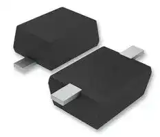
Zener Single Diode, Precision, 15 V, 200 mW, SOD-323, 2 Pins, 150 °C, Surface Mount
⚠️ Reference pricing provided. In case of supply shortages, we will connect you with our trusted procurement partners to ensure your project's continuity.
- Manufacturer: DIODES INC.
- Product type: Zener Single Diodes
- Zener Voltage Vz Typ:15V; Power Dissipation Pd:200mW; Diode Case Style:SOD-323; Zener Tolerance ±:5%; No. of Pins:2Pins; Operating Temperature Max:150°C; Product Range:DDZ97 Series; Auto
- SVHC: No SVHC (25-Jun-2025)
- No. of Pins: 2Pins
- Product Range: DDZ97
- Qualification: -
- Diode Mounting: Surface Mount
- Diode Case Style: SOD-323
- Power Dissipation: 200mW
- Zener Voltage Nom: 15V
- Operating Temperature Max: 150°C
| Delivery and price | |
|---|---|
| Units per pack | 1000 |
| Price | 0.048 € |
| Current stock | 1000+ |
| Lead time | 30 days |
Datasheet

Please click here to visit our online spice models database. Please click here to visit our online spice models database.

## **DDZ9689S - DDZ9717S** fo **SURFACE MOUNT PRECISION ZENER DIODE**

## **Features**

- Very Sharp Breakdown Characteristics

- Very Tight Tolerance on VZ

- Ideally Suited for Automated Assembly Processes

- Very Low Leakage Current

- **Lead Free By Design/RoHS Compliant (Note 1)**

- **“Green” Device (Note 2)**

## **Mechanical Data**

- Case: SOD-323

- Case Material: Molded Plastic, “Green” Molding Compound. UL Flammability Classification Rating 94V-0

- Moisture Sensitivity: Level 1 per J-STD-020

- Terminals: Finish - Matte Tin annealed over Alloy 42 leadframe. Solderable per MIL-STD-202, Method 208

- Polarity: Cathode Band

- Marking Information: See Page 6

- Ordering Information: See Page 6

- Weight: 0.004 grams (approximate)

**==> picture [30 x 8] intentionally omitted <==**

**----- Start of picture text -----**<br>
Top View<br>**----- End of picture text -----**<br>


**Maximum Ratings** @TA = 25°C unless otherwise specified

|**Maximum Ratingsgss** @TA = 25°C unless otherwise specifiedA = 25°C unless otherwise specified= 25°C unless otherwise specified|**Maximum Ratingsgss** @TA = 25°C unless otherwise specifiedA = 25°C unless otherwise specified= 25°C unless otherwise specified|**Maximum Ratingsgss** @TA = 25°C unless otherwise specifiedA = 25°C unless otherwise specified= 25°C unless otherwise specified|**Maximum Ratingsgss** @TA = 25°C unless otherwise specifiedA = 25°C unless otherwise specified= 25°C unless otherwise specified|
|---|---|---|---|
|||||
|**Characteristic**|**Symbol **|**Value**|**Unit**|
|Forward Voltage<br> @IF= 10mA|VF|0.9|V|


## **Thermal Characteristics**

|**Thermal Characteristics**||||
|---|---|---|---|
|**Characteristic**|**Symbol **|**Value**|**Unit**|
|Power Dissipation(Note 3)|PD|200|mW|
|Thermal Resistance,Junction to Ambient Air(Note 3)|RθJA|625|°C/W|
|Operatingand Storage Temperature Range|TJ,TSTG|-65 to +150|°C|


- Notes: 1. No purposefully added lead.

2. Diode’s Inc.’s “Green” policy can be found on our website at http://www.diodes.com/products/lead_free/index.php.

3. Device mounted on FR-4 PC board with recommended pad layout, which can be found on our website at http://www.diodes.com/datasheets/ap02001.pdf.

1 of 7 **www.diodes.com**

DDZ9689S - DDZ9717S Document number: DS30409 Rev. 6 - 2

August 2009 © Diodes Incorporated

|**Electrical Characteristics** @TA= 25°C unless otherwise specified|**Electrical Characteristics** @TA= 25°C unless otherwise specified|**Electrical Characteristics** @TA= 25°C unless otherwise specified|**Electrical Characteristics** @TA= 25°C unless otherwise specified|**Electrical Characteristics** @TA= 25°C unless otherwise specified|**Electrical Characteristics** @TA= 25°C unless otherwise specified|**Electrical Characteristics** @TA= 25°C unless otherwise specified|**Electrical Characteristics** @TA= 25°C unless otherwise specified|
|---|---|---|---|---|---|---|---|
|~~in~~||||||||
|**Type**<br>**Number**<br>~~in~~|**Type**<br>**Code**<br>~~in~~|**Zener Voltage Range (Note 3)**<br>~~in~~||||**Maximum Reverse**<br>**Leakage Current(Note 4)**<br>~~in~~||
|||**VZ @ IZT**<br>~~in~~|||**IZT**<br>~~in~~|**IR @ VR**<br>~~in~~||
|||**Nom(V)**<br>~~in~~|**Min(V)**<br>~~in~~|**Max(V)**<br>~~in~~|μ**A**<br>~~in~~|μ**A**<br>~~in~~|**V**<br>~~in~~|
|DDZ9689S<br>~~in~~|HH<br>~~in~~|5.1<br>~~in~~|4.85<br>~~in~~|5.36<br>~~in~~|50<br>~~in~~|5<br>~~in~~|3<br>~~in~~|
|DDZ9690S<br>~~in~~|HJ<br>~~in~~|5.6<br>~~in~~|5.32<br>~~in~~|5.88<br>~~in~~|50<br>~~in~~|2<br>~~in~~|4<br>~~in~~|
|DDZ9691S<br>~~in~~|HK<br>~~in~~|6.2<br>~~in~~|5.89<br>~~in~~|6.51<br>~~in~~|50<br>~~in~~|1<br>~~in~~|5<br>~~in~~|
|DDZ9692S<br>~~in~~|HL<br>~~in~~|6.8<br>~~in~~|6.46<br>~~in~~|7.14<br>~~in~~|50<br>~~in~~|0.1<br>~~in~~|5.1<br>~~in~~|
|DDZ9693S<br>~~in~~|HM<br>~~in~~|7.5<br>~~in~~|7.13<br>~~in~~|7.88<br>~~in~~|50<br>~~in~~|0.1<br>~~in~~|5.7<br>~~in~~|
|DDZ9694S<br>~~in~~|HN<br>~~in~~|8.2<br>~~in~~|7.79<br>~~in~~|8.61<br>~~in~~|50<br>~~in~~|0.1<br>~~in~~|6.2<br>~~in~~|
|DDZ9696S<br>~~in~~|HP<br>~~in~~|9.1<br>~~in~~|8.65<br>~~in~~|9.56<br>~~in~~|50<br>~~in~~|0.1<br>~~in~~|6.9<br>~~in~~|
|DDZ9697S<br>~~in~~|HQ<br>~~in~~|10<br>~~in~~|9.50<br>~~in~~|10.50<br>~~in~~|50<br>~~in~~|0.1<br>~~in~~|7.6<br>~~in~~|
|DDZ9698S<br>~~in~~|HR<br>~~in~~|11<br>~~in~~|10.45<br>~~in~~|11.55<br>~~in~~|50<br>~~in~~|0.05<br>~~in~~|8.4<br>~~in~~|
|DDZ9699S<br>~~in~~|HS<br>~~in~~|12<br>~~in~~|11.40<br>~~in~~|12.60<br>~~in~~|50<br>~~in~~|0.05<br>~~in~~|9.1<br>~~in~~|
|DDZ9700S<br>~~in~~|HT<br>~~in~~|13<br>~~in~~|12.35<br>~~in~~|13.65<br>~~in~~|50<br>~~in~~|0.05<br>~~in~~|9.8<br>~~in~~|
|DDZ9701S<br>~~in~~|HU<br>~~in~~|14<br>~~in~~|13.30<br>~~in~~|14.70<br>~~in~~|50<br>~~in~~|0.05<br>~~in~~|10.6<br>~~in~~|
|DDZ9702S<br>~~in~~|HV<br>~~in~~|15<br>~~in~~|14.25<br>~~in~~|15.75<br>~~in~~|50<br>~~in~~|0.05<br>~~in~~|11.4<br>~~in~~|
|DDZ9703S<br>~~in~~|HW<br>~~in~~|16<br>~~in~~|15.20<br>~~in~~|16.80<br>~~in~~|50<br>~~in~~|0.05<br>~~in~~|12.1<br>~~in~~|
|DDZ9705S(Note 5)<br>~~in~~|HY<br>~~in~~|18<br>~~in~~|17.10<br>~~in~~|18.90<br>~~in~~|50<br>~~in~~|0.05<br>~~in~~|13.6<br>~~in~~|
|DDZ9707S<br>~~in~~|MD<br>~~in~~|20<br>~~in~~|19.00<br>~~in~~|21.00<br>~~in~~|50<br>~~in~~|0.05<br>~~in~~|15.2<br>~~in~~|
|DDZ9708S<br>~~in~~|ME<br>~~in~~|22<br>~~in~~|20.90<br>~~in~~|23.10<br>~~in~~|50<br>~~in~~|0.05<br>~~in~~|16.7<br>~~in~~|
|DDZ9709S<br>~~in~~|MF<br>~~in~~|24<br>~~in~~|22.80<br>~~in~~|25.20<br>~~in~~|50<br>~~in~~|0.05<br>~~in~~|18.2<br>~~in~~|
|DDZ9711S<br>~~in~~|MH<br>~~in~~|27<br>~~in~~|25.65<br>~~in~~|28.35<br>~~in~~|50<br>~~in~~|0.05<br>~~in~~|20.4<br>~~in~~|
|DDZ9712S<br>~~in~~|MJ<br>~~in~~|28<br>~~in~~|26.60<br>~~in~~|29.40<br>~~in~~|50<br>~~in~~|0.05<br>~~in~~|21.2<br>~~in~~|
|DDZ9713S<br>~~in~~|MK<br>~~in~~|30<br>~~in~~|28.50<br>~~in~~|31.50<br>~~in~~|50<br>~~in~~|0.05<br>~~in~~|22.8<br>~~in~~|
|DDZ9714S<br>~~in~~|ML<br>~~in~~|33<br>~~in~~|31.35<br>~~in~~|34.65<br>~~in~~|50<br>~~in~~|0.05<br>~~in~~|25.0<br>~~in~~|
|DDZ9715S<br>~~in~~|MM<br>~~in~~|36<br>~~in~~|34.20<br>~~in~~|37.80<br>~~in~~|50<br>~~in~~|0.05<br>~~in~~|27.3<br>~~in~~|
|DDZ9716S<br>~~in~~|MN<br>~~in~~|39<br>~~in~~|37.05<br>~~in~~|40.95<br>~~in~~|50<br>~~in~~|0.05<br>~~in~~|29.6<br>~~in~~|
|DDZ9717S<br>~~in~~|MO<br>~~in~~|43<br>~~in~~|40.85<br>~~in~~|45.15<br>~~in~~|50<br>~~in~~|0.05<br>~~in~~|32.6<br>~~in~~|


**==> picture [210 x 214] intentionally omitted <==**

**----- Start of picture text -----**<br>
240<br>200<br>160<br>120<br>80<br>40<br>0<br>0 25 50 75 100 125 150<br>TA, AMBIENT TEMPERATURE (°C)<br>Fig. 1  Power Derating Curve<br>, POWER DISSIPATION (mW)<br>D<br>P<br>**----- End of picture text -----**<br>


**==> picture [226 x 216] intentionally omitted <==**

**----- Start of picture text -----**<br>
1,000<br>100<br>10<br>aeneee<br>1.0<br>Sanran<br>0.1<br>o p<br>0.01 f F<br>0 0.2 0.4 0.6 0.8 1.0 1.2<br>VF, INSTANTANEOUS FORWARD VOLTAGE (V)<br>Fig. 2  Typical Forward Characteristics<br>, INSTANTANEOUS FORWARD CURRENT (mA)<br>IF<br>**----- End of picture text -----**<br>


2 of 7 **www.diodes.com**

DDZ9689S - DDZ9717S Document number: DS30409 Rev. 6 - 2

August 2009 © Diodes Incorporated

**DDZ9689S - DDZ9717S**

**==> picture [363 x 188] intentionally omitted <==**

**----- Start of picture text -----**<br>
100m ggenvggeues epg<br>SB8esSeeeeF FSS g7§ §2 5/15a7 e-g7e5 5<br>10m<br>1m<br>— HAE EP<br>. THU aoe<br>100n<br>10n<br>0 5 10 15 20 25 30 35 40 45<br>, ZENER CURRENT (A)<br>IZ<br>**----- End of picture text -----**<br>


**==> picture [477 x 449] intentionally omitted <==**

**----- Start of picture text -----**<br>
100m a 100m<br>a ee es ee es eee —s DDZ9696Sa{———— es a |<br>10m pores | 10m i a es ee<br>1m _———————————aee eS Se eecs fi ee Ss|a nn | 1m SSeSes eeSSeS SSes|(eeeeS | | s Se |<br>4 00.f f 100. —|—J rors —<br>——— = |00z9607s =| 1 — =<br>eean eelee e — ft -p  f m008 |<br>40,ee ee eee 40, ff fo oos ff<br>tu —_ fF| | ff |0698s —f| tu _|ee| ee aea<br>ee A ee e e<br>100n Ae eee ee 100n ff ff tf ff esft<br>3.0 4.0 5.0 6.0 7.0 8.0 9.0 8.0 10.0 11.0 12.0 13.0 14.0 15.0<br>VZ, ZENER VOLTAGE (V) VZ, ZENER VOLTAGE (V)<br>Fig. 4  Typical Zener Breakdown Characteristics,  Fig. 5  Typical Zener Breakdown Characteristics,<br>DDZ9692S - DDZ9694S DDZ9696S - DDZ9701S<br>100m 100m<br>Be ——————————————<br>| | A A A e s<br>10m 10m<br>1m 1m<br>SSeeee | ee ee ee ee — ppz0707sDDz97078 etd— —<br>100—————————————— || a ———— —<br>——}-—f 0oz9708s ——F DDz9705S___ es es | ppz9709s —<br>101 ee ee ee ee 101 ee ee ee ee<br>SsffeSffeSeS SSS SS SSS —————_——————ee ee ee ee ||<br>tu e e e ee eee e ee tu __ | | iJ —J7| T J<br>Pp ee e e<br>100n —T | | 100n r | | ET] 7] |<br>14 15 16 17 18 19 20 19 20 21 22 23 24 25<br>VZ, ZENER VOLTAGE (V)Z, ZENER VOLTAGE (V), ZENER VOLTAGE (V) VZ, ZENER VOLTAGE (V)<br>Fig. 6  Typical Zener Breakdown Characteristics,  Fig. 7  Typical Zener Breakdown Characteristics,<br>DDZ9702S - DDZ9705S DDZ9707S - DDZ9709S<br>, ZENER CURRENT (A)<br>, ZENER CURRENT (A)IZ IZ<br>, ZENER CURRENT (A)<br>Z IZ<br>**----- End of picture text -----**<br>


**==> picture [220 x 218] intentionally omitted <==**

**----- Start of picture text -----**<br>
100m<br>Be<br>| | A A A<br>10m<br>1m<br>SSeeee | ee ee ee ee<br>100—————————————— ||<br>——}-—f 0oz9708s ——F DDz9705S___<br>101 ee ee ee ee<br>SsffeSffeSeS SSS SS SSS<br>tu e e e ee eee e ee<br>Pp<br>100n —T | |<br>14 15 16 17 18 19 20<br>VZ, ZENER VOLTAGE (V)Z, ZENER VOLTAGE (V), ZENER VOLTAGE (V)<br>Fig. 6  Typical Zener Breakdown Characteristics,<br>DDZ9702S - DDZ9705S<br>, ZENER CURRENT (A)<br>IZ<br>**----- End of picture text -----**<br>


3 of 7 **www.diodes.com**

DDZ9689S - DDZ9717S Document number: DS30409 Rev. 6 - 2

August 2009 © Diodes Incorporated

**DDZ9689S - DDZ9717S**

**==> picture [474 x 677] intentionally omitted <==**

**----- Start of picture text -----**<br>
100m a 100m a<br>(SC GS ee ee a |<br>Cr | | | [| |_ | a<br>10m 10m<br>SS wre ss |= = — —<br>1m a—f—f | | P f 1m Of| eozernes fa ee F<br>oon fe [ ee e e | ee $00 fo4} ozerirs + +<br>cf ||| [| 7 _] |<br>10u jo 10uee<br>a | a ee Oe ss<br>ee ee ee ee ee e e e e<br>I ee G O<br>100n ee eee eee 100n ss|<br>26 28 30 32 34 36 38 38 40 42 44 46 48 50<br>VZ, ZENER VOLTAGE (V)Z, ZENER VOLTAGE (V), ZENER VOLTAGE (V) VZ, ZENER VOLTAGE (V)<br>Fig. 8  Typical Zener Breakdown Characteristics,  Fig. 9  Typical Zener Breakdown Characteristics,<br>DDZ9711S - DDZ9715S DDZ9716S - DDZ9717S<br>100 10,000<br>TJ = 25 °C<br>f = 1MHz<br>=e. ee es ee r e<br>| 1,000 [ref<br>ee x VR =1V Mel —— NE<br>ee i e } e ee<br>Nee| e ow<br>VR = 2V we rs}2 100 CidLj]|z (|~n_Nn_)dSN N N<br>10 ee oO a O O ,<br>10<br>po Ww- es a  a|ee a<br>4 — » 1 | | | —<br>er | e e<br>SS| =Z  208<br>1 0.1<br>1 10 100 2 3 4 5 6 7<br>VZ, NOMINAL ZENER VOLTAGE (V) VZ, ZENER VOLTAGE (V)<br>Fig. 10 Total Capacitance vs. Nominal Zener Voltage Fig. 11  Typical Zener Impedance Characteristics,<br>DDZ9689S - DDZ9692S<br>10,000 a 10,000 Se ee<br>aa aOOOaGO aCf COr [TCSrCSC—CSSCSCS<SS—‘C*”r] O<br>1,000 1,000<br>— —————<br>a rs} a<br>100 100<br>_—— a I = 250A ———<br>eSse ee o= a a<br>10 a ee ee ee e a 10 I= 500A ___|_ [_}—___—___-_]<br>—$—$—— (| Ww a cs<br>2 Ni- — lL, =5mA a ee [|]<br>1 1<br>ee re<br>a aa<br>OC | a CO<br>a a (|<br>0.1 0.1<br>7 8 9 10 11 12 12 13 14 15 16 17 18<br>VZ, ZENER VOLTAGE (V) VZ, ZENER VOLTAGE (V)<br>Fig. 12  Typical Zener Impedance Characteristics,  Fig. 13  Typical Zener Impedance Characteristics,<br>DDZ9693S - DDZ9699S DDZ9699S - DDZ9705S<br>, ZENER CURRENT (A)<br>IZ<br>, TOTAL CAPACITANCE (pF)<br>T<br>C<br>**----- End of picture text -----**<br>


**==> picture [216 x 220] intentionally omitted <==**

**----- Start of picture text -----**<br>
100m a<br>(SC GS<br>Cr | | | [| |_ |<br>10m<br>SS wre ss |=<br>1m a—f—f | | P f<br>oon fe [ ee e e | ee<br>cf ||| [| 7 _]<br>10u jo<br>a |<br>ee ee ee ee ee e e<br>I<br>100n ee eee eee<br>26 28 30 32 34 36 38<br>VZ, ZENER VOLTAGE (V)Z, ZENER VOLTAGE (V), ZENER VOLTAGE (V)<br>Fig. 8  Typical Zener Breakdown Characteristics,<br>DDZ9711S - DDZ9715S<br>, ZENER CURRENT (A)<br>IZ<br>**----- End of picture text -----**<br>


4 of 7 **www.diodes.com**

DDZ9689S - DDZ9717S Document number: DS30409 Rev. 6 - 2

August 2009 © Diodes Incorporated

**DDZ9689S - DDZ9717S** ee

**==> picture [324 x 217] intentionally omitted <==**

**----- Start of picture text -----**<br>
10,000 ——$—————SS 10,000 _——a<br>a GG (|<br>a<br>1,000 ee ee e 1,000<br>SS ~— e S<br>po Ww<br>err O 1,<br>Zz<br>100 100<br>|= 500¢A $e— Sp<br>— ———\ = EEE —————<—<————<br>10 ——_a e a ————————t ra 10 |=Zo amaZo ama ama<br>ee ee 4 fT =zimtmA N~~ a<br>N<br>1 1<br>_<br>——— _—___—oOoO<br>a GG (| a<br>0.1 0.1<br>a ee ee<br>18 19 20 21 22 23 24 24<br>VZ, ZENER VOLTAGE (V)<br>Fig. 14  Typical Zener Impedance Characteristics,<br>DDZ9705S - DDZ9709S<br>**----- End of picture text -----**<br>


**==> picture [228 x 676] intentionally omitted <==**

**----- Start of picture text -----**<br>
10,000 _——a<br>a GC<br>EE ee<br>1,000 yes fo<br>~— e S A<br>Ww e<br>O 1, = 250A rs es<br>Zz Zz<br>100<br>Sp 2 8008= —————<br>= EEE —————<—<———— —_——<br>ra 10 |=Zo amaZo ama ama —eeeee e e<br>N~~ a<br>N<br>1<br>_—___—oOoO<br>a a<br>0.1<br>ee ee ee ee<br>24 26 28 30 32 34<br>VZ, ZENER VOLTAGE (V)<br>Fig. 15  Typical Zener Impedance Characteristics,<br>DDZ9709S - DDZ9714S<br>0.12<br>0.10<br>0.08<br>0.06 Iz7 = SMA<br>0.04 ZO, s0un<br>Se rs4 ZT Le<br>0.02 A<br>0 Pt; TT te t t<br>-0.02<br>-0.04<br>-0.06 Pittty yy<br>-0.08<br>0 2 4 6 8 10<br>VZ, ZENER VOLTAGE (V)<br>Fig. 17  Typical Temperature Coefficient of Zener<br>Voltage vs. Zener Voltage, DDZ9692S - DDZ9697S<br>0.12<br>0.100.08 free| | te<br>—_————<br>0.06 etFy | lay = SOWA Pt tt<br>0.04 Jt | aaa<br>0.02<br>0<br>-0.02<br>-0.04<br>-0.06<br>-0.08<br>20 22 24 26 28 30<br>VZ, ZENER VOLTAGE (V)<br>Fig. 19  Typical Temperature Coefficient of Zener<br>Voltage vs. Zener Voltage, DDZ9707S - DDZ9713S<br>, TEMPERATURE COEFFICIENT<br>Z<br>OF ZENER VOLTAGE (%/°C)<br>TC of V<br>, TEMPERATURE COEFFICIENT<br>Z<br>OF ZENER VOLTAGE (%/°C)<br>TC of V<br>**----- End of picture text -----**<br>


**==> picture [228 x 429] intentionally omitted <==**

**----- Start of picture text -----**<br>
10,000 o e<br>ly = 50pA = p<br>a |<br>1,000<br>~ Iz = 250pA S S<br>ie}4 a e e<br>Z 100 250A — |_| |_ |<br>=<a ——Zz i ————— Ss<br>a a ee |<br>Se ef 10 m<br>ZzWuWw __P Ee cem | Eo ff ||<br>N<br>N 1 SSS SSS SSS SS SS 8<br>Po<br>=SS [CL] SSS SS<br>0.1<br>34 36 38 40 42 44 46 48<br>VZ, ZENER VOLTAGE (V)<br>Fig. 16  Typical Zener Impedance Characteristics,<br>DDZ9715S - DDZ9716S<br>0.12<br>0.10<br>0.080.06 EE Pitt? SSee EEL a CT To<br>0.04<br>PTT tt | rer<br>0.02<br>0<br>-0.02<br>-0.04<br>-0.06<br>-0.08<br>10 12 14 16 18 20<br>VZ, ZENER VOLTAGE (V)<br>, TEMPERATURE COEFFICIENT<br>Z<br>OF ZENER VOLTAGE (%/°C)<br>TC of V<br>**----- End of picture text -----**<br>


Fig. 18  Typical Temperature Coefficient of Zener Voltage vs. Zener Voltage, DDZ9697S - DDZ9707S

5 of 7 **www.diodes.com**

DDZ9689S - DDZ9717S

August 2009 © Diodes Incorporated

Document number: DS30409 Rev. 6 - 2

**DDZ9689S - DDZ9717S**

**==> picture [228 x 221] intentionally omitted <==**

**----- Start of picture text -----**<br>
0.12<br>0.10<br>Hien {|| tf<br>0.08<br>0.06 tkPi<br>0.020.04 PtPit{|typtttttt ttett yt<br>0 P| ELL<br>-0.02 Pi |tTft | | tt |<br>-0.04 Pi te<br>-0.06 Pi ttt tt<br>-0.08 Pitt ELLE.<br>30 34 38 42 46 50<br>VZ, ZENER VOLTAGE (V)<br>Fig. 20  Typical Temperature Coefficient of Zener<br>Voltage vs. Zener Voltage, DDZ9713S - DDZ9716S<br>, TEMPERATURE COEFFICIENT<br>Z<br>OF ZENER VOLTAGE (%/°C)<br>TC of V<br>**----- End of picture text -----**<br>


## **Ordering Information** (Note 6)

|**Ordering Informationg Information Information** (Note 6)|||
|---|---|---|
|**Part Number**|**Case**|**Packaging**|
|(Type Number)-7*|SOD-323|3000/Tape & Reel|


*Example: The part number for the 6.2 Volt device would be DDZ9691S-7.

Notes: 6. For packaging details, go to our website at http://www.diodes.com/datasheets/ap02007.pdf.

## **Marking Information**

xx = Product Type Marking Code **XX** (See Electrical Characteristics Table)

## **Package Outline Dimensions**

**==> picture [375 x 218] intentionally omitted <==**

**----- Start of picture text -----**<br>
C<br>H<br>SOD-323<br>—— Dim  Min  Max<br>B A A  0.25 0.35<br>B  1.20 1.40<br>oy —+-—far<br>C 2.30 2.70<br>H  1.60  1.80<br>J  0.00  0.10<br>K  1.0 1.1<br>M K J L  0.20 0.40<br>L M  0.10 0.15<br>h© s 1iege α 0°  8°<br>All Dimensions in mm<br>FG )<br>DDZ9689S - DDZ9717S 6 of 7<br>Document number: DS30409 Rev. 6 - 2 www.diodes.com<br>**----- End of picture text -----**<br>


August 2009 © Diodes Incorporated

**DDZ9689S - DDZ9717S**

## **Suggested Pad Layout**

**==> picture [316 x 104] intentionally omitted <==**

**----- Start of picture text -----**<br>
C<br>— —<br>Dimensions Value (in mm)<br>Z  3.75<br>X G 1.05<br>X  0.65<br>Y  1.35<br>i:<br>C 2.40<br>Y G<br>Z<br>ot<br>**----- End of picture text -----**<br>


## **IMPORTANT NOTICE**

DIODES INCORPORATED MAKES NO WARRANTY OF ANY KIND, EXPRESS OR IMPLIED, WITH REGARDS TO THIS DOCUMENT, INCLUDING, BUT NOT LIMITED TO, THE IMPLIED WARRANTIES OF MERCHANTABILITY AND FITNESS FOR A PARTICULAR PURPOSE (AND THEIR EQUIVALENTS UNDER THE LAWS OF ANY JURISDICTION).

Diodes Incorporated and its subsidiaries reserve the right to make modifications, enhancements, improvements, corrections or other changes without further notice to this document and any product described herein. Diodes Incorporated does not assume any liability arising out of the application or use of this document or any product described herein; neither does Diodes Incorporated convey any license under its patent or trademark rights, nor the rights of others.  Any Customer or user of this document or products described herein in such applications shall assume all risks of such use and will agree to hold Diodes Incorporated and all the companies whose products are represented on Diodes Incorporated website, harmless against all damages.

Diodes Incorporated does not warrant or accept any liability whatsoever in respect of any products purchased through unauthorized sales channel. Should Customers purchase or use Diodes Incorporated products for any unintended or unauthorized application, Customers shall indemnify and hold Diodes Incorporated and its representatives harmless against all claims, damages, expenses, and attorney fees arising out of, directly or indirectly, any claim of personal injury or death associated with such unintended or unauthorized application.

Products described herein may be covered by one or more United States, international or foreign patents pending.  Product names and markings noted herein may also be covered by one or more United States, international or foreign trademarks.

## **LIFE SUPPORT**

Diodes Incorporated products are specifically not authorized for use as critical components in life support devices or systems without the express written approval of the Chief Executive Officer of Diodes Incorporated. As used herein:

A.   Life support devices or systems are devices or systems which:

1. are intended to implant into the body, or

2. support or sustain life and whose failure to perform when properly used in accordance with instructions for use provided in the labeling can be reasonably expected to result in significant injury to the user.

B.   A critical component is any component in a life support device or system whose failure to perform can be reasonably expected to cause the failure of the life support device or to affect its safety or effectiveness.

Customers represent that they have all necessary expertise in the safety and regulatory ramifications of their life support devices or systems, and acknowledge and agree that they are solely responsible for all legal, regulatory and safety-related requirements concerning their products and any use of Diodes Incorporated products in such safety-critical, life support devices or systems, notwithstanding any devices- or systems-related information or support that may be provided by Diodes Incorporated.  Further, Customers must fully indemnify Diodes Incorporated and its representatives against any damages arising out of the use of Diodes Incorporated products in such safety-critical, life support devices or systems.

Copyright © 2009, Diodes Incorporated

## **www.diodes.com**

7 of 7 **www.diodes.com**

DDZ9689S - DDZ9717S Document number: DS30409 Rev. 6 - 2

August 2009 © Diodes Incorporated
Updated at June 7, 2026
About Novapart
Novapart is a B2B electronic component broker specialising in stock shortages and cost reduction. We source hard-to-find parts and identify compliant alternatives across a catalogue of 410,000+ components from 500+ manufacturers.
Learn more →Stock Shortage Specialist
When a component is unavailable, discontinued or has an unacceptable lead time, we tap into our network of vetted European and Asian distributors to source what you need — without compromising on quality or traceability.
Request a quote →Compliant Alternatives
We identify pin-to-pin, electrically equivalent substitutes that meet the same certifications (RoHS, AEC-Q100, REACH) as your original specification — validated against datasheets, not just part numbers. Often at a lower cost.
BOM Analysis service →