
Image not available
Illustrative purposes only

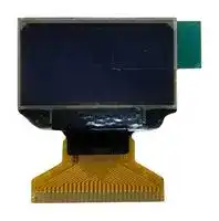
DD-12864WE-2A
Graphic OLED, 128 x 64 Pixels, Mono, 2.8V, I2C, Parallel, SPI, 26.7mm x 19.26mm, -40 °C
⚠️ Reference pricing provided. In case of supply shortages, we will connect you with our trusted procurement partners to ensure your project's continuity.
- Manufacturer: DENSITRON
- Product type: Graphic OLED Displays
- Resolution: 128 x 64 Pixels
- Module Size: 26.7mm x 19.26mm
- Logic Voltage: 2.8V
- Interface Type: I2C, Parallel, SPI
- Display Appearance: Mono
- Display Construction: COG
- Operating Temperature Max: 70°C
- Operating Temperature Min: -40°C
| Delivery and price | |
|---|---|
| Units per pack | 1 |
| Price | 5.84 € |
| Current stock | 25+ |
| Lead time | 7 days |
Datasheet

_OLED Dis la Module p y_ ~~ee)~~
## **DD-12864WE-2A**
## **PRODUCT SPECIFICATION**
Version 1.0 Mar 19, 2020
_Customer’s Approval Signature Date_
Prepared by _Chi Huang_ Approved by _Eric Wan_
©2020 Densitron Technologies Ltd.
_OLED Dis la Module p y_
~~`~~
## Revision Histor y
|**VERSION**|**DATE**||**DESCRIPTION**|**AUTHOR**|
|---|---|---|---|---|
|1.0|Mar 19, 2020|Initial Released||Chi Huang|
## Legal Notice
Copyright ©2020 Densitron Technologies Ltd
All information contained in this document is proprietary and confidential to Densitron Technologies Ltd and is subject to a non-disclosure agreement. Unauthorized use, duplication, modification or disclosure of this information by any means without prior consent of Densitron Technologies Ltd is prohibited.
Every effort has been made to ensure the accuracy of this document; however, Densitron Technologies Ltd accepts no responsibility for any inaccuracies, errors or omissions herein. Densitron Technologies Ltd reserves the right to change specifications without prior notice in its absolute discretion, to supply the best product possible. Where Densitron Technologies Ltd or any of its group companies has (i) made a change to a product to incorporate a specific customer requirement or (ii) has created a design to a customer’s specific requirements, in either case the customer will indemnify and hold the relevant Densitron entity harmless against any claim that delivery against such requirement breaches any intellectual property or other rights of any 3rd party.
All brands and trademarks are the property of their respective owners and are hereby fully acknowledged.
5760000189 DD-12864WE-2A Product SPEC v1.0
©2020 Densitron Technologies Ltd. Page 2 of 45
_OLED Dis la Module p y_
~~`~~
## Table of Contents
|**GENERAL DESCRIPTION ......................................................................................................................................... 5**|
|---|
|1.1<br>Introduction .................................................................................................................................................. 5|
|1.2<br>Main Features ............................................................................................................................................... 5|
|**MECHANICAL SPECIFICATION ................................................................................................................................ 6**|
|2.1<br>Mechanical Characteristics ........................................................................................................................... 6|
|2.2<br>Mechanical Drawing ...................................................................................................................................... 7<br>**ELECTRICAL SPECIFICATION OLED .......................................................................................................................... 8**<br>3.1<br>Absolute Maximum Ratings .......................................................................................................................... 8<br>3.2<br>DC Electrical Characteristics OLED ................................................................................................................ 9<br>3.3<br>Interface Pin Assignment ............................................................................................................................ 11<br>3.4<br>Block Diagram ............................................................................................................................................. 13<br>3.5<br>Timing Characteristics ................................................................................................................................. 13<br>**OPTICAL SPECIFICATION OLED ............................................................................................................................. 18**<br>4.1<br>Optical Characteristics ................................................................................................................................ 18<br>**FUNCTIONAL SPECIFICATION OLED ...................................................................................................................... 19**<br>5.1<br>Commands .................................................................................................................................................. 19<br>5.2<br>Power Down and Power Up Sequence ........................................................................................................ 19<br>5.3<br>Reset Circuit ................................................................................................................................................ 20<br>5.4<br>Application Circuit ....................................................................................................................................... 21<br>5.5<br>Actual Application Example OLED ............................................................................................................... 31<br>**PACKAGING ......................................................................................................................................................... 35**<br>**QUALITY ASSURANCE SPECIFICATION .................................................................................................................. 36**<br>7.1<br>Conformity .................................................................................................................................................. 36|
|7.2<br>Environment Required ................................................................................................................................ 36|
|7.3<br>Delivery Assurance ...................................................................................................................................... 36|
|7.4<br>Dealing with Customer Complaints ............................................................................................................. 41|
|**RELIABILITY SPECIFICATION ................................................................................................................................. 42**|
|8.1<br>Reliability Tests ............................................................................................................................................ 42|
|**HANDLING PRECAUTIONS.................................................................................................................................... 43**|
5760000189 DD-12864WE-2A Product SPEC v1.0
©2020 Densitron Technologies Ltd. Page 3 of 45
_OLED Dis la Module p y_
|~~~~|||||
|---|---|---|---|---|
|~~~~|9.1|Handling Precautions .................................................................................................................................. 43|||
||9.2|Storage Precautions .................................................................................................................................... 44|||
||9.3|Designing Precautions ................................................................................................................................. 44|||
||9.4|Operation Precautions ................................................................................................................................ 45|||
||9.5|Other Precautions ....................................................................................................................................... 45|||
5760000189 DD-12864WE-2A Product SPEC v1.0
©2020 Densitron Technologies Ltd. Page 4 of 45
_OLED Dis la Module p y_
~~`~~
## General Description
## 1.1 Introduction
This is 0.96” Size passive matrix OLED display with Anti-Glare polarizer. This display comes in white monochrome area colour and all-round view, has a resolution of 128 x 64, and the display module supports 8-bit 68XX/80XX Parallel, 3-/4wire SPI and I[2] C interface.
## 1.2 Main Features
Item Contents ~~LO~~ Display Format 128 x 64 Dots ~~e~~ ~~**e** e~~ Colour White Monochrome ~~ee~~ Overall Dimensions 26.70 (W) x 19.26 (H) x 1.45 (D) mm ~~eeee~~ Surface Treatment Anti-Glare ~~ee~~ Viewing Area 23.744 (W) x 12.864 (H) mm ~~en~~ Active Area 21.744 (W) x 10.864 (H) mm ~~ee~~ Display Mode Passive Matrix (0.96”) ~~ee~~ Duty ratio 1/64 ~~ee~~ Display Driver IC SSD1306 ~~a~~ Operating temperature -40°C ~ +70°C ~~a es~~ Storage temperature -40°C ~ +85°C ~~a~~ ROHS Compliant to RoHS 2.0 ~~a~~
5760000189 DD-12864WE-2A Product SPEC v1.0
©2020 Densitron Technologies Ltd. Page 5 of 45
_OLED Dis la Module p y_
~~`~~
## Mechanical Specification
## 2.1 Mechanical Characteristics
Item Characteristic Unit Display Format 128 x 64 Dots Overall Dimensions 26.70 (W) x 19.26 (H) x 1.45 (D) mm Viewing Area 23.744 (W) x 12.864 (H) mm ~~|~~ Active Area 21.744 (W) x 10.864 (H) mm ~~|~~ | | | Dot Size 0.154 (W) x 0.154 (H) mm ~~|~~ Dot Pitch 0.170 (W) x 0.170 (H) mm ~~|~~ | | | Weight 1.54± 10% g | | | | IC Controller/Driver SSD1306 ~~ee~~
5760000189 DD-12864WE-2A Product SPEC v1.0
©2020 Densitron Technologies Ltd. Page 6 of 45
_OLED Dis la Module p y_
~~me `~~ = ~~=—~~
## 2.2 Mechanical Drawing
5760000189 DD-12864WE-2A Product SPEC v1.0
©2020 Densitron Technologies Ltd. Page 7 of 45
_OLED Dis la Module p y_
~~`~~
## Electrical Specification OLED
## 3.1 Absolute Maximum Ratings
|Item|Symbol|Min|Max|Unit|Note|
|---|---|---|---|---|---|
|Supply Voltage for Logic|VDD<br>~~ee~~|-0.3<br>~~ee~~|4<br>~~ee~~|V|1, 2<br>~~ee~~<br>~~ee~~|
|Supply Voltage for Display<br>~~ee~~|Vcc<br>~~ee~~<br>~~ee~~<br>~~ee~~|0<br>~~ee~~<br>~~ee~~<br>~~ee~~|11<br>~~ee~~<br>~~ee~~<br>~~ee~~|V<br>~~ee~~<br>~~ee~~||
|Supply Voltage for DC/DC<br>~~ee~~|VDDB<br>~~ee ~~<br>~~ee~~<br>~~ee~~<br>~~eee~~|-0.3<br> ~~ee ~~<br>~~ee~~<br>~~ee~~<br>~~ee~~|5<br> ~~ee~~<br>~~ee~~<br>~~ee~~<br>~~ee~~|V<br>~~ee~~<br>~~ee~~<br>~~ee~~||
|Operating Temperature<br>~~ee~~|TOP<br>~~ee ~~<br>~~ee~~<br>~~eee~~|-40<br> ~~ee ~~<br>~~ee~~<br>~~ee~~|70<br> ~~ee~~<br>~~ee~~<br>~~ee~~|°C<br>~~ee~~<br>~~ee~~<br>~~ee~~|-<br>~~ee~~<br>~~ee~~|
|Storage Temperature<br>~~ee~~|TSTG<br>~~eee ~~<br>~~ee~~|-40<br> ~~ee ~~<br>~~ee~~|85<br> ~~ee ~~<br>~~ee~~|°C<br> ~~ee~~<br>~~ee~~|3<br>~~ee~~|
|Life Time (100 cd/m2)|-|10,000|-|hour|4|
|Life Time (80 cd/m2)<br>~~i~~|-<br>~~ee~~|30000<br>~~ee~~<br>~~i~~|-|hour|-|
|Life Time (60 cd/m2)<br>~~i~~|-<br>~~ee~~|50000<br>~~ee~~<br>~~i~~|-|hour||
- **Note 1:** All the above voltages are on the basis of “VSS = 0V”.
- **Note 2:** When this module is used beyond the above absolute maximum ratings, permanent breakage of the module may occur. Also, for normal operations, it is desirable to use this module under the conditions according to Section 3.2 “DC Electrical Characteristics OLED” and Section 4. “Optical Characteristics OLED”. If this module is used beyond these conditions, malfunctioning of the module can occur and the reliability of the module may deteriorate.
- **Note 3:** The defined temperature ranges do not include the polarizer. The maximum withstood temperature of the polarizer should be 80°C
- **Note 4:** VCC=9.0V, Ta=25°C, 50% Checkerboard.
Software configuration follows section 5.5.1 Initialization.
- End of lifetime is specified as 50% of initial brightness reached. The average operating lifetime at room temperature is estimated by the accelerated operation at high temperature conditions.
5760000189 DD-12864WE-2A Product SPEC v1.0
©2020 Densitron Technologies Ltd. Page 8 of 45
_OLED Dis la Module p y_
~~`~~
## 3.2 DC Electrical Characteristics OLED
## VCC Supplied Externally
|Item|Symbol|Condition|Min|Typ|Max|Unit|Note|
|---|---|---|---|---|---|---|---|
|Supply Voltage for Logic|VDD|-<br>~~77~~|1.65<br>~~77~~|2.8<br>~~77~~|3.3<br>~~77~~|V<br>|-<br>~~_~~|
|Supply Voltage for Display<br>(Supplied Externally)|VCC|Internal DC/DC Disable<br>~~77~~|8.5<br>~~77~~<br>~~ee~~|9.0<br>~~77~~<br>~~ee~~|9.5<br>~~77~~<br>~~ee~~|V<br>|1<br>~~_~~|
|High Level Input|VIH|-<br>~~77~~<br>~~ee~~|0.8 x VDD<br>~~77~~<br>~~ee~~<br>~~ee~~|-<br>~~77~~<br>~~ee~~<br>~~ee~~|VDD<br>~~77 ~~<br>~~ee~~<br>~~ee~~|V<br>|-<br> ~~_~~|
|Low Level Input|VIL|-<br>~~ee~~<br>~~FL~~<br>~~FE~~|0<br>~~ee~~<br>~~ee ~~<br>~~FL~~<br>~~FELAREN~~|-<br>~~ee~~<br> ~~ee~~<br>~~FL~~<br>~~LAREN~~|0.2 x VDD<br>~~ee~~<br>~~ee~~<br>~~FL~~<br>~~LAREN~~|V<br>~~IL~~|-<br>~~SE~~<br>~~IL~~|
|High Level Output|VOH|IOUT=100µA, 3.3MHZ<br>~~FL~~<br>~~FE~~|0.9 x VDD<br>~~FL~~<br>~~FELAREN~~|-<br>~~FL~~<br>~~LAREN~~|VDD<br>~~FL~~<br>~~LAREN~~|V<br>~~IL~~|-<br>~~SE~~<br>~~IL~~|
|Low Level Output|VOL|IOUT=100µA, 3.3MHZ<br>~~FE~~<br>~~ee~~<br>~~AN.~~|0<br>~~FE LAREN~~<br>~~ee~~<br>~~AN.~~|-<br>~~LAREN~~<br>~~ee~~<br>~~Vee~~|0.1 x VDD<br>~~LAREN~~<br>~~ee~~<br>~~Vee~~|V<br>~~IL~~<br>~~Vee~~|-<br>~~IL~~<br>~~eee~~<br>~~Vee~~|
|Operating Current for VDD|IDD|-<br>~~ee~~<br>~~AN.~~|-<br>~~ee~~<br>~~AN.~~|180<br>~~ee~~<br>~~Vee~~|300<br>~~ee~~<br>~~Vee~~|µA<br>~~Vee~~|-<br>~~eee~~<br>~~Vee~~|
|Operating Current for VCC<br>(VCCSupplied Externally)<br>||ICC<br>||-<br>~~AN.~~|-<br>~~AN. ~~|5.7<br> ~~Vee~~|7.1<br>~~Vee~~|mA<br>~~Vee~~|2<br>~~Vee~~|
|||-<br>|<br>ew|-<br>ew<br>||8.5<br>| ~~|~~|10.6<br>~~|~~|mA<br>~~|~~|3|
|||-|-|15.3|19.1.|mA|4|
|Sleep Mode Current for VDD<br>~~|~~<br>~~le~~|IDD, SLEEP<br>~~A~~|-<br>~~A~~|-<br>~~A~~|1<br>~~A~~|5<br>~~A~~|µA<br>~~A~~|-<br>~~A~~|
|Sleep Mode Current for VCC<br>~~|~~<br>~~le~~|ICC, SLEEP<br>~~A~~|-<br>~~A~~|-<br>~~A~~|2<br>~~A~~|10<br>~~A~~|µA<br>~~A~~|-<br>~~A~~|
**Note 1:** Brightness (Lbr) and Supply Voltage for Display (VCC) are subject to the change of the panel characteristics and the customer’s request.
**Note 2:** VDD = 2.8V, VCC = 9.0V, 30% Display Area Turn on.
**Note 3:** VDD = 2.8V, VCC = 9.0V, 50% Display Area Turn on.
**Note 4:** VDD = 2.8V, VCC = 9.0V, 100% Display Area Turn on.
*Software configuration follows section 5.5.1 Initialization
5760000189 DD-12864WE-2A Product SPEC v1.0
©2020 Densitron Technologies Ltd. Page 9 of 45
_OLED Dis la Module p y_
~~`~~
## VCC Generated by Internal DC/DC Circuit
|Item|Symbol|Condition|Min|Typ|Max|Unit|Note|
|---|---|---|---|---|---|---|---|
|Supply Voltage for Logic|VDD|-|1.65|2.8|3.3|V|-|
|Supply Voltage for DC/DC|VDDB|Internal DC/DC Enable|3.0|-|4.2|V|-|
|Supply Voltage for Display<br>(Generated by Internal DC/DC)|VCC|Internal DC/DC Enable|7.0|7.5|8.0|V|1|
|High Level Input|VIH|-|0.8 x VDD||VDD|V|-|
|Low Level Input|VIL|-|0||0.2 x VDD|V|-|
|High Level Output|VOH|IOUT=100µA, 3.3MHZ|0.9 x VDD|-|VDD|V|-|
|Low Level Output|VOL|IOUT=100µA, 3.3MHZ|0|-|0.1 x VDD|V|-|
|Operating Current for VDD|IDD|-|-|180|300|µA|-|
|Operating Current for VDDB<br>(VCCGenerated by Internal DC/DC)<br>~~|A~~<br>~~|~~|IDDB<br>~~|A~~<br>~~|~~|-<br>~~|A~~|-<br>~~|A~~|12.5<br>~~|A~~|15.6<br>~~|A~~|mA<br>~~|A~~|2<br>~~|A~~|
|||-<br>~~|~~<br>Lo|-<br>~~|~~<br>o<br>||17.8<br>~~|~~<br>||22.3|mA|3|
|||-|-|27.9|34.9|mA|4|
|Sleep Mode Current for VDD<br>~~a~~|IDD, SLEEP<br>~~a~~|-<br>~~ee~~|-<br>~~ee~~|1|5<br>~~ee~~|µA<br>~~ee~~|-<br>~~ee~~|
|Sleep Mode Current for VDDB<br>~~a~~|IDDB, SLEEP<br>~~a~~|-<br>~~ee~~|-<br>~~ee~~|2|10<br>~~ee~~|µA<br>~~ee~~|-<br>~~ee~~|
**Note 1:** Brightness (Lbr) and Supply Voltage for Display (VCC) are subject to the change of the panel characteristics and
the customer’s request.
**Note 2:** VDD = 2.8V, VDDB = 3.5V, VCC Generated by Internal DC/DC, 30% Display Area Turn on.
**Note 3:** VDD = 2.8V, VDDB = 3.5V, VCC Generated by Internal DC/DC, 50% Display Area Turn on.
**Note 4:** VDD = 2.8V, VDDB = 3.5V, VCC Generated by Internal DC/DC, 100% Display Area Turn on.
*Software configuration follows section 5.5.2 Initialization
5760000189 DD-12864WE-2A Product SPEC v1.0
©2020 Densitron Technologies Ltd. Page 10 of 45
_OLED Dis la Module p y_
~~`~~
## 3.3 Interface Pin Assignment
|No.|Symbol|I/O|Function|
|---|---|---|---|
|1|NC (GND)|-|-|
|2 / 3<br>4 / 5|C2P / C2N<br>C1P / C1N|I|**Positive Terminal of the Flying Inverting Capacitor**<br>**Negative Terminal of the Flying Boost Capacitor**<br>The charge-pump capacitors are required between the terminals.<br>Theymust be floated when the converter is not used.|
|6|VDDB|P|**Power Supply for DC/DC Converter Circuit**<br>This is the power supply pin for the internal buffer of the DC/DC voltage converter.<br>It must be connected to external source when the converter is used. It should be<br>connected to VDDwhen the converter is not used.|
|7<br>~~aS~~|NC<br>~~aS~~|-<br>~~aS~~|**Reserved Pin**<br>The N.C.pin between functionpins are reserved for compatible and flexible design.<br>~~aS~~|
|8<br>~~aS~~|VSS<br>~~aS~~|P<br>~~aS~~|**Ground of Logic Circuit**<br>This is a ground pin. It acts as a reference for the logic pins. It must be connected to<br>externalground.<br>~~aS~~|
|9<br>~~aS~~|VDD<br>~~aS~~|P<br>~~aS~~|**Power Supply for Logic**<br>This is a voltage supply pin. It must be connected to external source.<br>~~aS~~|
|10|BS0<br>BS1<br>BS2|I|**Communicating Protocol Select**<br>These pins are MCU interface selection input. See the following table:<br>BS0<br>BS1<br>BS2<br>I2C<br>3-wire SPI<br>4-wire SPI<br>8-bit 68XX Parallel<br>8-bit 80XX Parallel<br>0<br>1<br>0<br>0<br>0<br>1<br>0<br>0<br>0<br>1<br>0<br>0<br>0<br>1<br>1<br>~~cL~~|
|11<br>~~|~~||||
|12<br>~~|~~||||
|13<br>~~|~~|CS#|I|**Chip Select**<br>This pin is the chip select input. The chip is enabled for MCU communication only when<br>CS# ispulled low.<br>~~cL~~|
|14<br>~~|~~|RES#|O|**Power Reset for Controller and Driver**<br>This pin is reset signal input. When the pin is low, initialization of the chip is executed.<br>Keepthispinpull high duringnormal operation.<br>~~cL~~|
|15<br>~~|~~|D/C#|P|**Data/Command Control**<br>This pin is Data/Command control pin. When the pin is pulled high, the input at D7~D0<br>is treated as display data. When the pin is pulled low, the input at D7~D0 will be<br>transferred to the command register.<br>When the pin is pulled high and serial interface mode is selected, the data at SDIN will<br>be interpreted as data. When it is pulled low, the data at SDIN will be transferred to the<br>command register. In I2C mode, this pin acts as SA0 for slave address selection.<br>For detail relationshipto MCU interface signals, please refer to the Timing<br>~~cL~~|
5760000189 DD-12864WE-2A Product SPEC v1.0
©2020 Densitron Technologies Ltd. Page 11 of 45
_OLED Dis la Module p y_
|No.|Symbol|I/O|Function|
|---|---|---|---|
||||Characteristics Diagrams.|
|16|R/W#|I|**Read/Write Select or Write**<br>This pin is MCU interface input. When interfacing to a 68XX-series microprocessor, this<br>pin will be used as Read/Write (R/W#) selection input. Pull this pin to “High” for read<br>mode and pull it to “Low” for write mode.<br>When 80XX interface mode is selected, this pin will be the Write (WR#) input.<br>Data write operation is initiated when this pin is pulled low and the CS# is pulled low.<br>When serial or I2C mode is selected,thispin must be connected to VSS.|
|17<br>~~Le~~|E/RD#<br>~~Le~~|I<br>~~Le~~|**Read/Write Enable or Read**<br>This pin is MCU interface input. When interfacing to a 68XX-series microprocessor, this<br>pin will be used as the Enable (E) signal. Read/write operation is initiated when this pin<br>is pulled high and the CS# is pulled low.<br>When connecting to an 80XX-microprocessor, this pin receives the Read (RD#) signal.<br>Data read operation is initiated when this pin is pulled low and CS# is pulled low.<br>When serial or I2C mode is selected,thispin must be connected to VSS.<br>~~Le~~|
|18~25<br>~~Le~~|D0~D7<br>~~Le~~|I/O<br>~~Le~~|**Host Data Input / Output Bus**<br>These pins are 8-bit bi-directional data bus to be connected to the microprocessor’s<br>data bus. When serial mode is selected, D1 will be the serial data input SDIN and D0<br>will be the serial clock input SCLK. When I2C mode is selected, D2 & D1 should be tired<br>together and serve as SDAout& SDAinin application and D0 is the serial clock input SCL.<br>Unusedpins must be connected to VSSexcept for D2 in serial mode.<br>~~Le~~|
|26<br>~~Le~~|IREF<br>~~Le~~|I<br>~~Le~~|**Current Reference for Brightness Adjustment**<br>This pin is segment current reference pin. A resistor should be connected between this<br>pin and VSS. Set the current at 12.5μA maximum.<br>~~Le~~|
|27<br>|VCOMH<br>|O<br>|**Voltage Output High Level for COM Signal**<br>This pin is the input pin for the voltage output high level for COM signals. A capacitor<br>should be connected between thispin and VSS.<br>|
|28<br><br>~~—~~|VCC<br><br>~~—~~|P<br><br>~~—~~|**Power Supply for OEL Panel**<br>This is the most positive voltage supply pin of the chip. A stabilization capacitor should<br>be connected between this pin and VSSwhen the converter is used. It must be<br>connected to external source when the converter is not used.<br><br>~~—~~|
|29<br><br>~~—~~|VLSS<br><br>~~—~~|P<br><br>~~—~~|**Ground of Analog Circuit**<br>This is an analog groundpin. It should be connected to VSSexternally.<br><br>~~—~~|
|30<br><br>~~-~~|N.C.<br>(GND)<br><br>~~-~~|-<br><br>~~-~~|**Reserved Pin (Supporting Pin)**<br>The supporting pins can reduce the influences from stresses on the function pins.<br>Thesepins must be connected to externalground as the ESDprotection circuit.<br><br>~~-~~|
5760000189 DD-12864WE-2A Product SPEC v1.0
_OLED Dis la Module p y_
~~`~~
## 3.4 Block Diagram
Please refer to section 5.4 Application circuit
## 3.5 Timing Characteristics
## 68XX-Series MPU Parallel Interface Timing Characteristics
|Parameter|Symbol|Min|Typ.|Max|Unit|Condition|
|---|---|---|---|---|---|---|
|Clock Cycle Time|tCYCLE|300|-|-|ns|-|
|Address SetupTime|tAS|5|-|-|ns|-|
|Address Hold Time|tAH|0|-|-|ns|-|
|Write Data SetupTime|tDSW|40|-|-|ns|-|
|Write Data Hold Time|tDHW|7|-|-|ns|-|
|Read Data Hold Time|tDHR|20|-|-|ns|-|
|Output Disable Time|tOH|-|-|70|ns|-|
|Access Time|tACC|-|-|140|ns|-|
|Chip Select Low Pulse Width (Read)<br>ChipSelect Low Pulse Width(Write)|PWCSL|120<br>60|-|-|ns|-|
|Chip Select High Pulse Width (Read)<br>ChipSelect High Pulse Width(Write)|PWCSH|60<br>60|-|-|ns|-|
|Rise Time|tR|-|-|40|ns|-|
|Fall Time|tF|-|-|40|ns|-|
*(VDD - VSS = 1.65V to 3.3V, Ta = 25°C)
5760000189 DD-12864WE-2A Product SPEC v1.0
©2020 Densitron Technologies Ltd. Page 13 of 45
_OLED Dis la Module p y_
~~`~~
## 80XX-Series MPU Parallel Interface Timing Characteristics
|Parameter|Symbol|Min|Typ.|Max|Unit|Condition|
|---|---|---|---|---|---|---|
|Clock Cycle Time|tCYCLE|300|-|-|ns|-|
|Address Setup Time|tAS|10|-|-|ns|-|
|Address Hold Time|tAH|0|-|-|ns|-|
|Write Data Setup Time|tDSW|40|-|-|ns|-|
|Write Data Hold Time|tDHW|7|-|-|ns|-|
|Read Data Hold Time|tDHR|20|-|-|ns|-|
|Output Disable Time|tOH|-|-|70|ns|-|
|Access Time|tACC|-|-|140|ns|-|
|Read Low Time|tPWLR|120|-|-|ns|-|
|Write Low Time|tPWLW|60|-|-|ns|-|
|Read High Time|tPWHR|60|-|-|ns|-|
|Write High Time|tPWHW|60|-|-|ns|-|
|Chip Select Setup Time|tCS|0|-|-|ns|-|
|Chip Select Hold Time to Read Signal|tCSH|0|-|-|ns|-|
|Chip Select Hold Time|tCSF|20|-|-|ns|-|
|Rise Time|tR|-|-|40|ns|-|
|Fall Time|tF|-|-|40|ns|-|
*(VDD - VSS = 1.65V to 3.3V, Ta = 25°C)
**==> picture [319 x 9] intentionally omitted <==**
**----- Start of picture text -----**<br>
Read Timing Write Timing<br>**----- End of picture text -----**<br>
5760000189 DD-12864WE-2A Product SPEC v1.0
©2020 Densitron Technologies Ltd. Page 14 of 45
_OLED Dis la Module p y_
~~`~~
## Serial Interface Timing Characteristics (4-wire SPI)
|Parameter|Symbol|Min|Typ.|Max|Unit|Condition|
|---|---|---|---|---|---|---|
|Clock Cycle Time|tcycle|100|-|-|ns|-|
|Address Setup Time|tAS|15|-|-|ns|-|
|Address Hold Time|tAH|15|-|-|ns|-|
|Chip Select Setup Time|tCSS|20|-|-|ns|-|
|Chip Select Hold Time|tCSH|10|-|-|ns|-|
|Write Data Setup Time|tDSW|15|-|-|ns|-|
|Write Data Hold Time|tDHW|15|-|-|ns|-|
|Clock Low Time|tCLKL|20|-|-|ns|-|
|Clock High Time|tCLKH|20|-|-|ns|-|
|Rise Time|tR|-|-|40|ns|-|
|Fall Time|tF|-|-|40|ns|-|
5760000189 DD-12864WE-2A Product SPEC v1.0
©2020 Densitron Technologies Ltd. Page 15 of 45
_OLED Dis la Module p y_
~~`~~
## Serial Interface Timing Characteristics (3-wire SPI)
|Parameter|Symbol|Min|Typ.|Max|Unit|Condition|
|---|---|---|---|---|---|---|
|Clock Cycle Time|tcycle|100|-|-|ns|-|
|Chip Select Setup Time|tCSS|20|-|-|ns|-|
|Chip Select Hold Time|tCSH|10|-|-|ns|-|
|Write Data Setup Time|tDSW|15|-|-|ns|-|
|Write Data Hold Time|tDHW|15|-|-|ns|-|
|Clock Low Time|tCLKL|20|-|-|ns|-|
|Clock High Time|tCLKH|20|-|-|ns|-|
|Rise Time|tR|-|-|40|ns|-|
|Fall Time|tF|-|-|40|ns|-|
*(VDD - VSS = 1.65V to 3.3V, Ta = 25°C)
5760000189 DD-12864WE-2A Product SPEC v1.0
©2020 Densitron Technologies Ltd. Page 16 of 45
_OLED Dis la Module p y_
~~`~~
## I[2] C Interface Timing Characteristics:
|Parameter|Symbol|Min|Typ.|Max|Unit|Condition|
|---|---|---|---|---|---|---|
|Clock Cycle Time|tcycle|2.5|-|-|μs|-|
|Start Condition Hold Time|tHSTART|0.6|-|-|μs|-|
|Data Hold Time (for “SDAOUT” Pin)|tHD|0|-|-|ns|-|
|Data Hold Time (for “SDAIN” Pin)|tHD|300|||ns||
|Data Setup Time|tSD|100|-|-|ns|-|
|Start Condition Setup Time<br>(Only relevant for a repeated Start condition)|tSSTART|0.6|-|-|μs|-|
|Stop Condition Setup Time|tSSTOP|0.6|-|-|μs|-|
|Rise Time for Data and Clock Pin|tR|-|-|300|ns|-|
|Fall Time for Data and Clock Pin|tF|-|-|300|ns|-|
|Idle Time before a New Transmission can Start|tIDLE|1.3|-|-|μs|-|
*(VDD - VSS = 1.65V to 3.3V, Ta = 25°C)
5760000189 DD-12864WE-2A Product SPEC v1.0
©2020 Densitron Technologies Ltd. Page 17 of 45
**==> picture [517 x 326] intentionally omitted <==**
**----- Start of picture text -----**<br>
Densitron<br>OLED Dis la Module<br>p y<br>`<br>Optical Specification OLED<br>4.1 Optical Characteristics<br>Characteristics Symbol Conditions Min Typ Max Unit Note<br>Brightness<br>Lbr - 100 120 - cd/m [2] 1<br>(VCC Supplied Externally)<br>Brightness<br>Lbr - 70 90 - cd/m [2] 2<br>(VCC Generated by Internal DC/DC)<br>(x) 0.24 0.27 0.30<br>C.I.E. (White) C.I.E. 1931 - -<br>= (y) 0.27 0.30 0.33<br>Dark Room Contrast CR - - >10,000:1 - - -<br>tA Viewing Angle - - - Free - - degree<br>*Optical measurement taken at (1) VDD = 2.8V, VCC = 9V & 7.5V.<br>**----- End of picture text -----**<br>
*Software configuration follows Section 5.5.1 Initialization
**Note 1:** Brightness (Lbr) and Supply Voltage for Display (VCC) are subject to the change of the panel characteristics and the customer’s request.
**Note 2:** VDD = 2.8V, VCC = 9.0V, 30% Display Area Turn on.
5760000189 DD-12864WE-2A Product SPEC v1.0
©2020 Densitron Technologies Ltd. Page 18 of 45
_OLED Dis la Module p y_
~~a `~~
## Functional Specification OLED
## 5.1 Commands
Refer to the Technical Manual for the SSD1306.
## 5.2 Power Down and Power Up Sequence
To protect OEL panel and extend the panel life time, the driver IC power up/down routine should include a delay period between high voltage and low voltage power sources during turn on/off. It gives the OEL panel enough time to complete the action of charge and discharge before/after the operation.
- 5.2.1 Power up Sequence Voo/ Voos on 1. Power up VDD / VDDB Display
- 2. Send Display off command 3. Initialization VCC 4. Clear Screen 5. Power up VCC VDD/VDDB 6. Delay 100ms (When VCC is stable) VSS/Ground TIee 7. Send Display on command 5.2.2 Power down Sequence DisplayVeooff/ Vonr Off 1. Send Display off command 2. Power down VCC / VDDB VCC/VDDB 3. Delay 100ms (When VCC / VDDB is reach 0 and panel is completely discharged) VDD
- 4. Power down VDD VSS/Ground
## **Note:**
1. Since an ESD protection circuit is connected between VDD and VCC inside the driver IC, VCC becomes lower than VDD whenever VDD is ON and VCC is OFF.
2. VCC / VDDB should be kept float (disable) when it is OFF.
3. Power Pins (VDD, VCC, VDDB) can never be pulled to ground under any circumstance.
4. VDD should not be power down before VCC / VDDB power down.
5760000189 DD-12864WE-2A Product SPEC v1.0
©2020 Densitron Technologies Ltd. Page 19 of 45
_OLED Dis la Module p y_
~~`~~
## 5.3 Reset Circuit
When RES# input is low, the chip is initialized with the following status:
1. Display is OFF
2. 128 x 64 Display Mode
3. Normal segment and display data column and row address mapping (SEG0 mapped to column address 00h and COM0 mapped to row address 00h)
4. Shift register data clear in serial interface
5. Display start line is set at display RAM address 0
6. Column address counter is set at 0
7. Normal scan direction of the COM outputs
8. Contrast control register is set at 7Fh
9. Normal display mode (Equivalent to A4h command)
5760000189 DD-12864WE-2A Product SPEC v1.0
©2020 Densitron Technologies Ltd. Page 20 of 45
_OLED Dis la Module p y_ ~~me ` =~~
## 5.4 Application Circuit
## 68XX-Series MPU Parallel Interface and VCC Supplied Externally
5760000189 DD-12864WE-2A Product SPEC v1.0
©2020 Densitron Technologies Ltd. Page 21 of 45
_OLED Dis la Module p y_
~~`~~
## 68XX-Series MPU Parallel Interface and VCC Generated by Internal
## DC/DC Circuit
5760000189 DD-12864WE-2A Product SPEC v1.0
©2020 Densitron Technologies Ltd. Page 22 of 45
_OLED Dis la Module p y_
~~a `~~
## 80XX-Series MPU Parallel Interface and VCC Supplied Externally
5760000189 DD-12864WE-2A Product SPEC v1.0
©2020 Densitron Technologies Ltd. Page 23 of 45
_OLED Dis la Module p y_
~~`~~
## 80XX-Series MPU Parallel Interface and VCC Generated by Internal
## DC/DC Circuit
5760000189 DD-12864WE-2A Product SPEC v1.0
©2020 Densitron Technologies Ltd. Page 24 of 45
_OLED Dis la Module p y_ ~~me ` =~~
## 4-wire Serial Interface and VCC Supplied Externally
5760000189 DD-12864WE-2A Product SPEC v1.0
©2020 Densitron Technologies Ltd. Page 25 of 45
_OLED Dis la Module p y_ ~~me ` =~~
## 4-wire Serial Interface and VCC Generated by Internal DC/DC Circuit
5760000189 DD-12864WE-2A Product SPEC v1.0
©2020 Densitron Technologies Ltd. Page 26 of 45
_OLED Dis la Module p y_
~~me ` =~~
## 3-wire Serial Interface and VCC Supplied Externally
5760000189 DD-12864WE-2A Product SPEC v1.0
©2020 Densitron Technologies Ltd. Page 27 of 45
## _OLED Dis la Module p y_ ~~me ` =~~ 5.4.8 3-wire Serial Interface and VCC Generated by Internal DC/DC Circuit
5760000189 DD-12864WE-2A Product SPEC v1.0
©2020 Densitron Technologies Ltd. Page 28 of 45
_OLED Dis la Module p y_
~~`~~
## I[2] C Interface and VCC Supplied Externally
5760000189 DD-12864WE-2A Product SPEC v1.0
©2020 Densitron Technologies Ltd. Page 29 of 45
_OLED Dis la Module p y_ ~~me ` =~~
## I2C Interface and VCC Generated by Internal DC/DC Circuit
5760000189 DD-12864WE-2A Product SPEC v1.0
©2020 Densitron Technologies Ltd. Page 30 of 45
_OLED Dis la Module p y_
~~aa `~~
## 5.5 Actual Application Example OLED
Command usage and explanation of an actual example
## VCC Supplied Externally
**==> picture [95 x 9] intentionally omitted <==**
**----- Start of picture text -----**<br>
<Power up Sequence><br>**----- End of picture text -----**<br>
If the noise is accidentally occurred at the displaying window during the operation, please reset the display in order to recover the display function.
5760000189 DD-12864WE-2A Product SPEC v1.0
©2020 Densitron Technologies Ltd. Page 31 of 45
_OLED Dis la Module p y_
**==> picture [560 x 385] intentionally omitted <==**
**----- Start of picture text -----**<br>
aa `<br><Power down Sequence><br>Normal Operation Power down Voc Voo/ Vcc offState<br>P (100ms Delay Recommended) DOP ee<br>Set Display Off<br><Entering Sleep Mode><br>set pispiay Off Sleep Mode<br><Exiting Sleep Mode><br>**----- End of picture text -----**<br>
5760000189 DD-12864WE-2A Product SPEC v1.0
©2020 Densitron Technologies Ltd. Page 32 of 45
_OLED Dis la Module p y_
~~aa `~~
## VCC Generated by Internal DC/DC Circuit
**==> picture [95 x 9] intentionally omitted <==**
**----- Start of picture text -----**<br>
<Power up Sequence><br>**----- End of picture text -----**<br>
If the noise is accidentally occurred at the displaying window during the operation, please reset the display in order to recover the display function.
5760000189 DD-12864WE-2A Product SPEC v1.0
©2020 Densitron Technologies Ltd. Page 33 of 45
_OLED Dis la Module p y_
**==> picture [560 x 439] intentionally omitted <==**
**----- Start of picture text -----**<br>
aa `<br><Power down Sequence><br>Normal . Power Stabilized<br> Operation (100ms Delay Recommended) Vov/ Vong off State<br>Set Display Off Power down Vopps<br>OxAE (50ms Delay Recommended)<br>Set Charge Pump<br><Entering Sleep Mode><br>Normal Operation aD OxID Sleep Mode<br>Set Display Off Power down V<br>OxAE pe<br><Exiting Sleep Mode><br>**----- End of picture text -----**<br>
5760000189 DD-12864WE-2A Product SPEC v1.0
©2020 Densitron Technologies Ltd. Page 34 of 45
_OLED Dis la Module p y_
~~Oo `~~
## Packaging
|Item|Quantity|
|---|---|
|Module|1080<br>per Primary Box|
|Holding Trays<br>(A)|20<br>per Primary Box|
|Total Trays<br>(B)|21<br>per Primary Box (Including 1 Empty Tray)|
|Primary Box<br>(C)|1~4<br>per Carton (4 as Major / Maximum)|
5760000189 DD-12864WE-2A Product SPEC v1.0
©2020 Densitron Technologies Ltd. Page 35 of 45
_OLED Dis la Module p y_
~~`~~
## Quality Assurance Specification
## 7.1 Conformity
The performance, function and reliability of the shipped products conform to the Product Specification.
## 7.2 Environment Required
Customer’s test & measurement are required to be conducted under the following conditions: Temperature: 23 ± 5°C Humidity: 55% ± 15% RH Fluorescent Lamp: 30W Distance between the Panel & Lamp: ≥ 50cm Distance between the Panel & Eyes of the Inspector: ≥ 30cm Finger glove (or finger cover) must be worn by the inspector. Inspection table or jig must be anti-electrostatic.
## 7.3 Delivery Assurance
## Delivery Inspection Standards
Level II, Normal Inspection, Single Sampling, MIL-STD-105E
## Criteria & Acceptable Quality Level
**==> picture [487 x 80] intentionally omitted <==**
**----- Start of picture text -----**<br>
7.3.2 Criteria & Acceptable Quality Level<br>Partition AQL Definition<br>Major 0.65 Defects in Pattern Check (Display On)<br>a<br>**----- End of picture text -----**<br>
Partition AQL Definition Major 0.65 Defects in Pattern Check (Display On) Minor 1.0 Defects in Cosmetic Check (Display Off)
5760000189 DD-12864WE-2A Product SPEC v1.0
©2020 Densitron Technologies Ltd. Page 36 of 45
_OLED Dis la Module p y_
~~`~~
## 7.3.2.1 Cosmetic Check (Display Off) in Non-Active Area
**==> picture [445 x 534] intentionally omitted <==**
**----- Start of picture text -----**<br>
Check Item Classification Criteria<br>i<br>X > 6 mm (Along with Edge)<br>Y > 1 mm (Perpendicular to edge)<br>Panel General Chipping Minor<br>Any crack is not allowable<br>Panel Crack Minor<br>NG<br>Copper Exposed<br>Minor Not Allowable by Naked Eye Inspection<br>(Even Pin or Film)<br>Film or Trace Damage Minor<br>**----- End of picture text -----**<br>
5760000189 DD-12864WE-2A Product SPEC v1.0
©2020 Densitron Technologies Ltd. Page 37 of 45
_OLED Dis la Module p y_
**==> picture [396 x 325] intentionally omitted <==**
**----- Start of picture text -----**<br>
`<br>Check Item Classification Criteria<br>Terminal Lead Prober Mark Acceptable<br>Glue or Contamination on Pin<br>(Couldn’t Be Removed by Minor<br>Alcohol)<br>Ink Marking on Back Side of<br>Acceptable Ignore for Any<br>panel (Exclude on Film)<br>**----- End of picture text -----**<br>
5760000189 DD-12864WE-2A Product SPEC v1.0
©2020 Densitron Technologies Ltd. Page 38 of 45
_OLED Dis la Module p y_
~~aa `~~
## 7.3.2.2 Cosmetic Check (Display Off) in Active Area
It is recommended to execute in clear room environment (class 10k) if actual in necessary.
|Check Item|Classification|Criteria|Criteria|
|---|---|---|---|
|Any Dirt & Scratch on Polarizer’s<br>Protective Film|Acceptable|Ignore for not Affect the Polarizer||
|Scratches, Fiber, Line-Shape Defect<br>(On Polarizer)|Minor|W ≤ 0.1<br>W > 0.1,<br>L ≤ 2<br>L > 2|Ignore<br>n ≤ 1<br>n = 0|
|Dirt, Black Spot, Foreign Material<br>(On Polarizer)|Minor|Φ≤0.1<br>0.1 < Φ≤0.25<br>0.25 < Φ|Ignore<br>n ≤ 1<br>n = 0|
|Dent, Bubbles, White spot<br>(Any Transparent Spot on Polarizer)|Minor|Φ≤0.5<br>0.5 < Φ|Ignore if no Influence<br>on Display<br>n = 0|
|||eke tesa<br>eae es<br>es!<br>a OY,C.DoeeRe<br>¢<br>a<br>* ae,ee<br>-||
|Fingerprint, Flow Mark<br>(On Polarizer)|Minor|Not Allowable||
**Note 1:** Protective film should not be tear off when cosmetic check.
**Note 2:** Definition of W & L & Φ (Unit: mm): Φ = (a + b) / 2
**==> picture [265 x 95] intentionally omitted <==**
**----- Start of picture text -----**<br>
L<br>b: Minor Axis<br>W<br>a: Major Axis<br>**----- End of picture text -----**<br>
5760000189 DD-12864WE-2A Product SPEC v1.0
©2020 Densitron Technologies Ltd. Page 39 of 45
_OLED Dis la Module p y_
~~`~~
## 7.3.2.3 Pattern Check (Display On) in Active Area
**==> picture [352 x 569] intentionally omitted <==**
**----- Start of picture text -----**<br>
Check Item Classification Criteria<br>No Display Major<br>a ete ee ee ee ee se ee ee ees one ese ee ee<br>eC<br>saatatatetctatatatatatatatetstataratete<br>atee se eae SH e See A 8 8 S88 e Boe a esse eee 8<br>Missing Line Major<br>ntatatatatutatatatatstetstatalstetatets<br>ntataatattatatntatatatatatalatetatets<br>unne<br>Pixel Short Major<br>Darker Pixel Major<br>Bereta<br>Hssrntntatatetatntatatetntatate<br>Neetetatatatatetatatatetatatate<br>Wrong Display Major<br>AHatatatatatatatetatytatatetatstatatetcietatatetstst<br>BHM<br>BERS RM BSR BA<br>tilethe<br>ee<br>Un-uniform Major paciieiaiaa:SID<br>**----- End of picture text -----**<br>
**==> picture [201 x 7] intentionally omitted <==**
**----- Start of picture text -----**<br>
5760000189 DD-12864WE-2A Product SPEC v1.0<br>**----- End of picture text -----**<br>
©2020 Densitron Technologies Ltd. Page 40 of 45
_OLED Dis la Module p y_
~~`~~
## 7.4 Dealing with Customer Complaints
## Non-conforming Analysis
Purchaser should supply Densitron with detailed data of non-conforming sample.
After accepting it, Densitron should complete the analysis in two weeks from receiving the sample.
If the analysis cannot be completed on time, Densitron must inform the purchaser.
## Handling of Non-conforming Displays
If any non-conforming displays are found during customer acceptance inspection which Densitron is clearly responsible for, return them to Densitron.
Both Densitron and customer should analyse the reason and discuss the handling of non-conforming displays when the reason is not clear.
Equally, both sides should discuss and come to agreement for issues pertaining to modification of Densitron quality assurance standard.
5760000189 DD-12864WE-2A Product SPEC v1.0
©2020 Densitron Technologies Ltd. Page 41 of 45
_OLED Dis la Module p y_
~~`~~
## Reliability Specification
## 8.1 Reliability Tests
**==> picture [479 x 139] intentionally omitted <==**
**----- Start of picture text -----**<br>
Test Item Test Condition Inspection After Test<br>High Temperature Operating 70℃, 240 hrs<br>Low Temperature Operating -40℃, 240 hrs<br>ee High Temperature Storage 85℃, 240 hrs<br>Low Temperature Storage -40℃, 240 hrs<br>The operational functions work.<br>High Temperature &<br>+60℃, 90% RH, 120 hours.<br>High Operating<br>-40℃ ↔ 85℃, 24 Cycles,<br>Thermal Shock (Non-operation)<br>60 min dwell.<br>**----- End of picture text -----**<br>
**Note 1:** The samples used for the above tests do not include polarizer.
**Note 2:** No moisture condensation is observed during tests.
## Failure Check Standard
After the completion of the described reliability test, the samples were left at room temperature for 2 hrs prior to conducting the failure teat at 23±5 °C ; 55±15% RH.
5760000189 DD-12864WE-2A Product SPEC v1.0
©2020 Densitron Technologies Ltd. Page 42 of 45
_OLED Dis la Module p y_
~~`~~
## Handling Precautions
## 9.1 Handling Precautions
- 1) Since the display panel is being made of glass, do not apply mechanical impacts such us dropping from a high position.
- 2) If the display panel is broken by some accident and the internal organic substance leaks out, be careful not to inhale nor lick the organic substance.
- 3) If pressure is applied to the display surface or its neighborhood of the OEL display module, the cell structure may be damaged and be careful not to apply pressure to these sections.
- 4) The polarizer covering the surface of the OEL display module is soft and easily scratched. Please be careful when handling the OEL display module.
- 5) When the surface of the polarizer of the OEL display module has soil, clean the surface. It takes advantage of by using following adhesion tape.
- a. Scotch Mending Tape No. 810 or an equivalent
- b. Never try to breathe upon the soiled surface nor wipe the surface using cloth containing solvent such as ethyl alcohol, since the surface of the polarizer will become cloudy.
- c. Also, pay attention that the following liquid and solvent may spoil the polarizer:
- Water
- Ketone
- Aromatic Solvents
- 6) Hold OEL display module very carefully when placing OEL display module into the system housing. Do not apply excessive stress or pressure to OEL display module. And, do not over bend the film with electrode pattern layouts. These stresses will influence the display performance. Also, secure sufficient
rigidity for the outer cases.
- 7) Do not apply stress to the LSI chips and the surrounding molded sections.
- 8) Do not disassemble nor modify the OEL display module.
- 9) Do not apply input signals while the logic power is off.
- 10) Pay sufficient attention to the working environments when handing OEL display modules to prevent occurrence of element breakage accidents by static electricity.
5760000189 DD-12864WE-2A Product SPEC v1.0
©2020 Densitron Technologies Ltd. Page 43 of 45
_OLED Dis la Module p y_
~~`~~
- Be sure to make human body grounding when handling OEL display modules.
- Be sure to ground tools to use or assembly such as soldering irons.
- To suppress generation of static electricity, avoid carrying out assembly work under dry environments.
- Protective film is being applied to the surface of the display panel of the OEL display module. Be careful since static electricity may be generated when exfoliating the protective film.
- 11) Protection film is being applied to the surface of the display panel and removes the protection film before assembling it. At this time, if the OEL display module has been stored for a long period of time, residue adhesive material of the protection film may remain on the surface of the display panel after removed of the film. In such case, remove the residue material by the method introduced in the above Section 5).
- 12) If electric current is applied when the OEL display module is being dewed or when it is placed under high humidity environments, the electrodes may be corroded and be careful to avoid the above.
## 9.2 Storage Precautions
- 1) When storing OEL display modules, put them in static electricity preventive bags avoiding exposure to direct sun light nor to lights of fluorescent lamps, etc. and, also, avoiding high temperature and high humidity environments or low temperature (less than 0°C) environments. (We recommend you to store these modules in the packaged state when they were shipped from Densitron Technologies Plc.) At that time, be careful not to let water drops adhere to the packages or bags nor let dewing occur with them.
- 2) If electric current is applied when water drops are adhering to the surface of the OEL display module, when the OEL display module is being dewed or when it is placed under high humidity environments, the electrodes may be corroded and be careful about the above.
## 9.3 Designing Precautions
- 1) The absolute maximum ratings are the ratings which cannot be exceeded for OEL display module, and if these values are exceeded, panel damage may be happen.
- 2) To prevent occurrence of malfunctioning by noise, pay attention to satisfy the VIL and VIH specifications and, at the same time, to make the signal line cable as short as possible.
- 3) We recommend you to install excess current preventive unit (fuses, etc.) to the power circuit (VDD). (Recommend value: 0.5A)
- 4) Pay sufficient attention to avoid occurrence of mutual noise interference with the neighboring devices.
- 5) As for EMI, take necessary measures on the equipment side basically.
- 6) When fastening the OEL display module, fasten the external plastic housing section.
5760000189 DD-12864WE-2A Product SPEC v1.0
©2020 Densitron Technologies Ltd. Page 44 of 45
_OLED Dis la Module p y_
~~`~~
- 7) If power supply to the OEL display module is forcibly shut down by such errors as taking out the main battery while the OEL display panel is in operation, we cannot guarantee the quality of this OEL display module.
- 8) The electric potential to be connected to the rear face of the IC chip should be as follows: US2066
*Connection (contact) to any other potential than the above may lead to rupture of the IC.
## 9.4 Operation Precautions
- 1) When an OEL display module is operated for a long of time with fixed pattern may remain as an after image or slight contrast deviation may occur. Nonetheless, if the operation is interrupted and left unused for a while, normal state can be restored. Also, there will be no problem in the reliability of the module.
- 2) To protect OEL display modules from performance drops by static electricity rapture, etc., do not touch the following sections whenever possible while handling the OEL display modules.
- a. Pins and electrodes
- b. Pattern layouts such as the FPC
- 3) With this OEL display module, the OEL driver is being exposed. Generally speaking, semiconductor elements change their characteristics when light is radiated according to the principle of the solar battery. Consequently, if this OEL driver is exposed to light, malfunctioning may occur.
- a. Design the product and installation method so that the OEL driver may be shielded from light in actual usage.
- b. Design the product and installation method so that the OEL driver may be shielded from light during the inspection processes.
- 4) Although this OEL display module stores the operation state data by the commands and the indication data, when excessive external noise, etc. enters into the module, the internal status may be changed. It therefore is necessary to take appropriate measures to suppress noise generation or to protect from influences of noise on the system design.
- 5) We recommend you to construct its software to make periodical refreshment of the operation statuses (re-setting of the commands and re-transference of the display data) to cope with catastrophic noise.
## 9.5 Other Precautions
- 1) Request the qualified companies to handle industrial wastes when disposing of the OEL display modules. Or, when burning them, be sure to observe the environmental and hygienic laws and regulations.
5760000189 DD-12864WE-2A Product SPEC v1.0
©2020 Densitron Technologies Ltd. Page 45 of 45
Updated at February 9, 2023
About Novapart
Novapart is a B2B electronic component broker specialising in stock shortages and cost reduction. We source hard-to-find parts and identify compliant alternatives across a catalogue of 410,000+ components from 500+ manufacturers.
Learn more →Stock Shortage Specialist
When a component is unavailable, discontinued or has an unacceptable lead time, we tap into our network of vetted European and Asian distributors to source what you need — without compromising on quality or traceability.
Request a quote →Compliant Alternatives
We identify pin-to-pin, electrically equivalent substitutes that meet the same certifications (RoHS, AEC-Q100, REACH) as your original specification — validated against datasheets, not just part numbers. Often at a lower cost.
BOM Analysis service →