


CYW20835PB1KML1GGF
Bluetooth Module, 2.4GHz, Bluetooth LE 5.2, 2 Mbps, -94.5 dBm, 1.62 to 3.63 VDC, -30 °C to 85 °C
- Manufacturer: INFINEON
- Product type: Bluetooth Modules & Adaptors
- SVHC: No SVHC (25-Jun-2025)
- Interfaces: I2C, SPI, UART
- Product Range: AIROC Series
- Certifications: -
- Bluetooth Class: Class 1
- Bluetooth Version: Bluetooth LE 5.2
- Supply Voltage Range: 1.62 VDC to 3.63 VDC
- Receiver Sensitivity Rx: -94.5 dBm
- Operating Temperature Range: -30 °C to 85 °C
| Delivery and price | |
|---|---|
| Units per pack | 500 |
| Price | 1.57 € |
| Current stock | 200+ |
| Lead time | 30 days |
**CYW20835** - A/™“| q **AIROC™ Bluetooth® LE system on chip** The AIROC™ CYW20835 Bluetooth® LE SoC is a Bluetooth® 5.2 core spec compliant device for IoT applications. Manufactured using the industry’s advanced 40-nm CMOS low-power process, the CYW20835 employs high levels of integration to minimize external components, reducing the device footprint and the costs associated with implementing Bluetooth® Low Energy solutions.
The AIROC™ CYW20835 Bluetooth® LE SoC is designed to support the wide spectrum of Bluetooth® Low Energy use cases for home automation, accessory, sensors (medical, home, security, and industrial), lighting, Bluetooth® Mesh, wireless input devices, and remote controls, or any Bluetooth® LE connected IoT application.
## **Features**
- Bluetooth® subsystem
- Complies with Bluetooth® core specification v5.2 with LE 2-Mbps support
- Bluetooth® Low Energy
- Supports adaptive frequency hopping (AFH)
- Programmable TX power up to 12 dBm
- Rx sensitivity -94.5 dBm (Bluetooth® LE)
- Ultra-low-power radio
- RX current 8 mA
- TX current 18 mA @ 12 dBm
- Coexistence support
- Support for global coexistence interface for easy coexistence implementation with select Infineon AIROC™ Wi-Fi devices
- MCU subsystem
- 96-MHz Arm® Cortex®-M4 microcontroller unit MCU with floating point unit (FPU)
- Supports Serial Wire Debug (SWD)
- Runs Bluetooth® stack and application
- Memory subsystem
- 384-KB RAM
- 2-MB ROM
- Audio features and interfaces
- 1x I2S with master and slave modes
- 1x PCM
- PDM
- Analog front end for analog microphone
- Clocks
- On chip 32-kHz oscillator
- On chip 128-kHz oscillator
- 32-kHz crystal oscillator
- 24-MHz crystal oscillator
- 32-bit real time clock (RTC)
Please read the Important Notice and Warnings at the end of this document page 1
Datasheet www.infineon.com
002-33561 Rev. *B
2023-01-18
## **AIROC™ Bluetooth® LE system on chip**
## Features
- Peripherals and communication
- 6x 16-bit PWMs
- Programmable key-scan matrix interface, up to 8x20 key-scanning matrix
- Quadrature decoder
- Watchdog timer
- 1x peripheral UART, 1x UART for programming and HCI
- 1x SPI (master or slave mode)
- 1x I2C master
- One ADC (10-ENoB for DC measurement and 12-ENOB for audio measurement)
- Hardware security engine
- General-purpose input output (GPIO)
- 24 GPIOs
- 2 dedicated pins for analog microphone
- Support 1.7 V to 3.63 V operation
- Four GPIOs support 16 mA and 8 mA source at 3.3 V and 1.8 V respectively
- Operating voltage and low-power support
- Wide operating voltage range - 1.625 V to 3.63 V
- 4 power modes to implement ultra-low power application - managed by real time operating system
- 1 A current in HID-Off mode
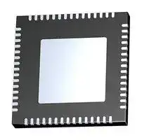
- Packages
- 7 mm x 7 mm 60-pin quad flat no-lead (QFN)
- Software support
- ModusToolbox™ software: Features are subject to support in the Bluetooth® SDK
- Check the latest version of the Bluetooth® SDK technical brief for supported features
- Applications
- Bluetooth® Mesh
- Wireless pointing devices (mice)
- Remote controls
- Joysticks
- Home automation
- Point-of-sale input devices
- Blood pressure monitors
- Find-me devices
- Heart-rate monitors
- Proximity sensors
- Thermometers
Datasheet
002-33561 Rev. *B
2
2023-01-18
**AIROC™ Bluetooth® LE system on chip**
Functional block diagram
## **Functional block diagram**
**==> picture [365 x 302] intentionally omitted <==**
**----- Start of picture text -----**<br>
Bluetooth® Core Microcontroller Subsystem<br>RAM<br>320 KB<br>Bluetooth LE Bluetooth LE<br>PA RF PHY MAC<br>ROM<br>2 MB<br>Arm®<br>Patch Control<br>Cortex® M4<br>96 MHz Patch RAM<br>Clocks w/ FPU 64 KB<br>XTAL OSC<br>24-MHz Debug UART/SWD<br>HP-LPO Watchdog<br>32kHz<br>XTAL OSC<br>32-kHz<br>LP-LPO<br>16/32/128-kHz<br>Peripherals<br>ADC TRNG GPIOs (24)<br>Power Management<br>Core DC-DC IR TRIAC I2C Master I/<br>O<br>RF LDO PWM (x6) Timer Analog MIC M<br>U<br>3-Axis<br>Digital LDO 3D Glass UART X<br>Quad.<br>PA LDO Keyscan PCM/I2S Q-SPI (x2)<br>(x2)<br>PDM<br>Coexistence Interface (GCI)<br>AHB Bus Matrix<br>**----- End of picture text -----**<br>
Datasheet
002-33561 Rev. *B
3
2023-01-18
**AIROC™ Bluetooth® LE system on chip**
Table of contents
## **Table of contents**
**Features ...........................................................................................................................................1 Functional block diagram...................................................................................................................3 Table of contents...............................................................................................................................4 1 Bluetooth® Baseband Core (BBC)......................................................................................................6** 1.1 Link control layer ....................................................................................................................................................6 1.2 Test mode support..................................................................................................................................................7 1.3 Frequency hopping generator ...............................................................................................................................7 1.4 Microprocessor unit................................................................................................................................................7 1.4.1 Floating point unit ...............................................................................................................................................7 1.4.2 OTP memory ........................................................................................................................................................7 1.4.3 NVRAM configuration data and storage..............................................................................................................7 1.4.4 Power-on reset (POR) ..........................................................................................................................................8 1.4.5 External reset .......................................................................................................................................................8 1.4.6 Brownout detection (BOD)..................................................................................................................................8 1.5 Power management unit (PMU).............................................................................................................................9 1.6 Integrated radio transceiver...................................................................................................................................9 1.6.1 Transmit path.......................................................................................................................................................9 1.6.2 Digital modulator.................................................................................................................................................9 1.6.3 Power amplifier....................................................................................................................................................9 1.6.4 Receiver path .......................................................................................................................................................9 1.6.5 Digital demodulator and bit synchronizer..........................................................................................................9 1.6.6 Receiver signal strength indicator ....................................................................................................................10 1.6.7 Local oscillator...................................................................................................................................................10 1.6.8 Calibration..........................................................................................................................................................10 1.7 Peripheral transport unit......................................................................................................................................10 1.7.1 I2C compatible master ......................................................................................................................................10 1.7.2 HCI UART interface.............................................................................................................................................10 1.8 Peripheral UART interface....................................................................................................................................11 1.9 Clock frequencies..................................................................................................................................................12 1.9.1 Crystal oscillator ................................................................................................................................................12 1.9.2 HID peripheral block..........................................................................................................................................12 1.9.3 32-kHz crystal oscillator ....................................................................................................................................13 1.10 GPIO ports ...........................................................................................................................................................13 1.11 Keyboard scanner...............................................................................................................................................14 1.11.1 Theory of operation.........................................................................................................................................14 1.11.2 Idle....................................................................................................................................................................14 1.11.3 Scan ..................................................................................................................................................................14 1.11.4 Scan end...........................................................................................................................................................14 1.12 Mouse quadrature signal decoder .....................................................................................................................15 1.12.1 Theory of operation.........................................................................................................................................15 1.13 ADC port ..............................................................................................................................................................15 1.14 PWM.....................................................................................................................................................................16 1.15 Triac control........................................................................................................................................................16 1.16 Serial peripheral interface (SPI).........................................................................................................................16 1.17 Infrared modulator .............................................................................................................................................17 1.18 PDM microphone ................................................................................................................................................17 1.19 Security engine ...................................................................................................................................................17 1.20 Power management unit....................................................................................................................................18 1.20.1 RF power management ...................................................................................................................................18 1.20.2 Host controller power management ..............................................................................................................18 1.20.3 BBC power management.................................................................................................................................18
Datasheet
002-33561 Rev. *B
4
2023-01-18
## **AIROC™ Bluetooth® LE system on chip**
Table of contents
**2 Pin assignments and GPIOs............................................................................................................19** 2.1 Pin assignments....................................................................................................................................................19 2.2 GPIO pin descriptions...........................................................................................................................................20 2.3 Pinouts ..................................................................................................................................................................23 2.3.1 60-pin QFN package...........................................................................................................................................23 **3 Electrical specifications.................................................................................................................24** 3.1 Electrical characteristics ......................................................................................................................................24 3.1.1 Core buck regulator...........................................................................................................................................25 3.1.2 Digital LDO..........................................................................................................................................................27 3.1.3 PA LDO................................................................................................................................................................28 3.1.4 RF LDO ................................................................................................................................................................29 3.1.5 Digital I/O characteristics ..................................................................................................................................30 3.1.6 Current consumption ........................................................................................................................................30 3.2 ADC electrical characteristics...............................................................................................................................30 3.3 RF specifications ...................................................................................................................................................32 3.4 Timing and AC characteristics..............................................................................................................................34 3.4.1 UART timing .......................................................................................................................................................34 3.4.2 SPI timing ...........................................................................................................................................................35 3.4.3 I2C interface timing............................................................................................................................................37 **4 Package diagram ..........................................................................................................................40** 4.1 Tray packaging specifications..............................................................................................................................41 **5 Ordering information....................................................................................................................42 6 Additional information..................................................................................................................43** 6.1 IoT resources.........................................................................................................................................................43 **7 Acronyms.....................................................................................................................................44 Revision history ..............................................................................................................................45**
Datasheet
002-33561 Rev. *B 2023-01-18
5
**AIROC™ Bluetooth® LE system on chip** BS
Bluetooth® Baseband Core (BBC)
## **1 Bluetooth® Baseband Core (BBC)**
The BBC implements all of the time-critical functions required for high-performance Bluetooth® operation. The BBC manages the buffering, segmentation, and routing of data for all connections. It also buffers data that passes through it, handles data flow control, schedules ACL and TX/RX transactions, monitors Bluetooth® slot usage, optimally segments and packages data into baseband packets, manages connection status indicators, and composes and decodes HCI packets. In addition to these functions, it independently handles HCI event types, and HCI command types. **Table 1** lists the major Bluetooth® SIG specification features supported by the CYW20835.
|**Bluetooth® 4.0**|**Bluetooth® 4.1**<br>~~OO~~|**Bluetooth® 4.2**|
|---|---|---|
|Bluetooth® Low Energy|Low duty cycle advertising<br>~~OO~~<br>~~OO~~|Data packet length extension|
|–|LE link layer topology<br>~~OO~~<br>~~OO~~|LE secure connection|
|–|–<br>~~OO~~|LE privacy 1.2|
|**Bluetooth® 5.0**|~~oO~~||
|Bluetooth® LE 2-Mbps|~~oO~~<br>~~OO~~||
|Slot availability mask (SAM)|~~OO~~<br>~~OO~~||
|LE channel selection|~~OO~~||
|High duty cycle non-connectable<br>advertisement|~~ee~~||
## **1.1**
## **Link control layer**
The link control layer is part of the Bluetooth® link control functions that are implemented in dedicated logic in the link control unit (LCU).
This layer consists of the command controller that takes commands from the software, and other controllers that are activated or configured by the command controller, to perform the link control tasks. Each task is performed in a different state or substate in the Bluetooth® link controller.
- Bluetooth® LE states
- Advertising
- Scanning
- Connection
- Major states
- Standby
- Connection
- Substates
- Page
- Page scan
- Inquiry
- Inquiry scan
- Sniff
Datasheet
002-33561 Rev. *B
6
2023-01-18
**AIROC™ Bluetooth® LE system on chip**
Bluetooth® Baseband Core (BBC)
## **1.2 Test mode support**
The CYW20835 fully supports Bluetooth® test mode as described in Part I:1 of the specification of the Bluetooth® system version 3.0. This includes the transmitter tests, normal and delayed loopback tests, and reduced hopping sequence.
In addition to the standard Bluetooth® test mode, the CYW20835 also supports enhanced testing features to simplify RF debugging and qualification and type-approval testing. These features include:
- Fixed frequency carrier wave (unmodulated) transmission
- Simplifies some type-approval measurements (Japan)
- Aids in transmitter performance analysis
- Fixed frequency constant receiver mode
- Receiver output directed to I/O pin
- Allows for direct BER measurements using standard RF test equipment
- Facilitates spurious emissions testing for receive mode
- Fixed frequency constant transmission
- 8-bit fixed pattern or PRBS-9
- Enables modulated signal measurements with standard RF test equipment
## **1.3 Frequency hopping generator**
The frequency hopping sequence generator selects the correct hopping channel number based on the link controller state, Bluetooth® clock, and device address.
## **1.4**
## **Microprocessor unit**
The CYW20835 microprocessor unit runs software from the link control (LC) layer up to the host controller interface (HCI). The microprocessor is a Cortex **®** -M4 32-bit RISC processor with embedded ICE-RT debug and Serial Wire Debug (SWD) interface units. The microprocessor also includes 2 MB of ROM memory for Bluetooth® stack and drivers for on-chip peripherals and 384 KB of RAM for data scratch-pad.
The internal ROM provides flexibility during power-on reset to enable the same device to be used in various configurations. At power-up, the lower-layer protocol stack is executed from internal ROM.
External patches can be applied to the ROM-based firmware to provide flexibility for bug fixes and feature additions. The device also supports the integration of user applications and profiles.
## **1.4.1 Floating point unit**
CYW20835 includes the CM4 single precision IEEE-754 compliant floating point unit. For details see the Cortex®-M4 manual.
## **1.4.2 OTP memory**
The CYW20835 includes 2 KB of one-time programmable memory that can be used by the factory to store product-specific information.
**Note** : Use of OTP requires that a 3 V supply be present at all times.
## **1.4.3 NVRAM configuration data and storage**
NVRAM contains configuration information about the customer application, including the following:
- Fractional-N information
- BD_ADDR
- UART baud rate
- SDP service record
- File system information used for code, code patches, or data. The CYW20835 uses SPI flash for NVRAM storage.
Datasheet
002-33561 Rev. *B 2023-01-18
7
## **AIROC™ Bluetooth® LE system on chip**
Bluetooth® Baseband Core (BBC)
## **1.4.4 Power-on reset (POR)**
The CYW20835 includes POR logic to allow the part to initialize correctly when power is applied. **Figure 2** shows the sequence used by the CYW20835 during initialization. An small external cap may be used on RESET_N to add delay as VDDIO ramps up.
## **1.4.5 External reset**
An external active-low reset signal, RESET_N, can be used to put the CYW20835 in the reset state.
**==> picture [328 x 285] intentionally omitted <==**
**----- Start of picture text -----**<br>
RESET_N<br>(External)<br>>= 2.4 ms (*1)<br>VDDIO ~190 us<br>(*2)<br>VDDC<br>~2 LPO cycles<br>VDDIO POR<br>8 LPO cycles<br>VDDC Reset<br>(Internal)<br>~2 LPO cycles<br>XTAL_PU ~30 LPO cycles<br>XTAL_BUF_PU<br>**----- End of picture text -----**<br>
- *1: External RESET_N is only effective 2.4 ms after VDDIO power is up
- *2: The latency depends on the value of DEFAULT_STRAP. If DEFAULT_STRAP is high, it s ~190 us.
- If DEFAULT_STRAP is low, it s ~250 us.
## **Figure 2 Power-on reset timing**
## **1.4.6 Brownout detection (BOD)**
An external voltage detector reset IC may be used if brownout detection is required. The reset IC should release RESET_N only after the VDDO supply voltage level has been at or above a minimum operating voltage for 50 ms or longer.
Datasheet
002-33561 Rev. *B
8
2023-01-18
**AIROC™ Bluetooth® LE system on chip**
Bluetooth® Baseband Core (BBC)
## **1.5 Power management unit (PMU)**
**Figure 3** shows the CYW20835 power management unit (PMU) block diagram. The CYW20835 includes an integrated buck regulator, a capless LDO, PALDO and an additional 1.2 V LDO for RF.
**==> picture [271 x 178] intentionally omitted <==**
**----- Start of picture text -----**<br>
PMU<br>50 mA SR_VLX<br>SR_VDDBAT3V CBUCK<br>SR_VBF<br>DIGLDO<br>DIGLDO_VDDIN1P5 (Capless, with 30 mA DIGLDO_VDDOUT<br>bypass mode)<br>o_vddout_digldo<br>RFLDO_VDDIN1P5 RFLDO 20 mA RFLDO_VDDOUT<br>XX] PMU_AVSS<br>PALDO_VDDIN_5V PALDO PALDO_VDDOUT3V<br>NOTE: x = Bump/Ball<br>**----- End of picture text -----**<br>
## **Figure 3 Power management unit**
## **1.6 Integrated radio transceiver**
The CYW20835 has an integrated radio transceiver that has been optimized for use in 2.4 GHz Bluetooth® wireless systems. It has been designed to provide low-power, low-cost, robust communications for applications operating in the globally available 2.4 GHz unlicensed ISM band. The CYW20835 is fully compliant with the Bluetooth® radio specification and meets or exceeds the requirements to provide the highest communication link quality of service.
## **1.6.1 Transmit path**
The CYW20835 features a fully integrated transmitter. The baseband transmit data is GFSK modulated in the 2.4 GHz ISM band.
## **1.6.2 Digital modulator**
The digital modulator performs the data modulation and filtering required for the GFSK signal. The fully digital modulator minimizes any frequency drift or anomalies in the modulation characteristics of the transmitted signal.
## **1.6.3 Power amplifier**
The CYW20835 has an integrated power amplifier (PA) that can transmit up to +12 dBm for class 1 operations.
## **1.6.4 Receiver path**
The receiver path uses a low-IF scheme to downconvert the received signal for demodulation in the digital demodulator and bit synchronizer. The receiver path provides a high degree of linearity, an extended dynamic range to ensure reliable operation in the noisy 2.4 GHz ISM band. The front-end topology, with built-in out-of-band attenuation, enables the CYW20835 to be used in most applications with minimal off-chip filtering.
## **1.6.5 Digital demodulator and bit synchronizer**
The digital demodulator and bit synchronizer takes the low-IF received signal and performs an optimal frequency tracking and bit-synchronization algorithm.
Datasheet
002-33561 Rev. *B 2023-01-18
9
**AIROC™ Bluetooth® LE system on chip**
Bluetooth® Baseband Core (BBC)
## **1.6.6 Receiver signal strength indicator**
The radio portion of the CYW20835 provides a receiver signal strength indicator (RSSI) signal to the baseband, so that the controller can take part in a Bluetooth® power-controlled link by providing a metric of its own receiver signal strength to determine whether the transmitter should increase or decrease its output power.
## **1.6.7 Local oscillator**
A local oscillator (LO) generation provides fast frequency hopping (1600 hops/second) across the 40 maximum available channels. The CYW20835 uses an internal loop filter.
## **1.6.8 Calibration**
The CYW20835 radio transceiver features a self-contained automated calibration scheme. No user interaction is required during normal operation or during manufacturing to provide optimal performance. Calibration compensates for filter, matching network, and amplifier gain and phase characteristics to yield radio performance within 2% of what is optimal. Calibration takes process and temperature variations into account, and it occurs transparently during normal operation and hop setting times.
## **1.7 Peripheral transport unit**
## **1.7.1 I[2] C compatible master**
The CYW20835 provides a 2-pin I2C compatible master interface to communicate with I2C compatible peripherals. I[2] C does not support multi-master capability or flexible wait-state insertion by either master or slave devices.
The following transfer clock rates are supported by I[2] C:
- 100 kHz
- 400 kHz
- 800 kHz (Not a standard I[2] C-compatible speed.)
- 1 MHz (Compatibility with high-speed I[2] C-compatible devices is not guaranteed).
The clock pin (SCL) and data pin (SDA) are both open-drain I/O pins. Pull-up resistors external to the CYW20835 are required on both the SCL and SDA pins for proper operation.
## **1.7.2 HCI UART interface**
The CYW20835 includes a UART interface for factory programming and when operating as a Bluetooth® HCI device in a system with an external host. The UART physical interface is a standard, 4-wire interface (RX, TX, RTS, and CTS) with adjustable baud rates from 57600 bps to 6 Mbps. During initial boot, UART speeds may be limited to 750 kbps. The baud rate may be selected via a vendor-specific UART HCI command. The CYW20835 has a 1040-byte receive FIFO and a 1040-byte transmit FIFO to support enhanced data rates. The interface supports the Bluetooth® UART HCI (H4) specification. The default baud rate for H4 is 115.2 kbaud.
The UART clock default setting is 24 MHz, and can be configured to run as high as 48 MHz to support up to 6 Mbps. The baud rate of the CYW20835 UART is controlled by two values. The first is a UART clock divisor (set in the DLBR register) that divides the UART clock by an integer multiple of 16. The second is a baud rate adjustment (set in the DHBR register) that is used to specify a number of UART clock cycles to stuff in the first or second half of each bit time. Up to eight UART cycles can be inserted into the first half of each bit time, and up to eight UART clock cycles can be inserted into the end of each bit time.
**Table 2** contains example values to generate common baud rates with a 24 MHz UART clock.
Datasheet
002-33561 Rev. *B 2023-01-18
10
## **AIROC™ Bluetooth® LE system on chip**
Bluetooth® Baseband Core (BBC)
|**Table 2**<br>**Common baud rate examples, 24 MHz clock**|**Common baud rate examples, 24 MHz clock**<br>~~——~~|**Common baud rate examples, 24 MHz clock**<br>~~——~~|||
|---|---|---|---|---|
|**Baud rate (bps)**|**Baud rate adjustment**<br>~~_~~<br>~~——~~||**Mode**|**Error (%)**|
||**High nibble**<br>~~——~~|**Low nibble**|||
|3M|0xFF<br>~~——~~|0xF8|High rate|0.00|
|2M|0XFF<br>~~es~~|0XF4<br>~~es~~|High rate<br>~~es~~|0.00|
|1M|0X44<br>~~es~~<br>~~es~~|0XFF<br>~~es~~<br>~~es~~|Normal<br>~~es~~<br>~~es~~|0.00|
|921600|0x05<br>~~es~~|0x05<br>~~es~~|Normal<br>~~es~~|0.16|
|460800|0x02<br>~~es~~|0x02<br>~~es~~|Normal<br>~~es~~|0.16|
|230400|0x04<br>~~es~~|0x04<br>~~es~~|Normal<br>~~es~~|0.16|
|115200|0x00<br>~~es~~<br>~~es~~|0x00<br>~~es~~<br>~~es~~|Normal<br>~~es~~<br>~~es~~|0.16|
|57600|0x00|0x00|Normal|0.16|
**Table 3** contains example values to generate common baud rates with a 48 MHz UART clock.
|**Baud rate (bps)**|**High rate**<br>~~es~~|**Low rate**<br>~~es~~|**Mode**<br>~~es~~|**Error (%)**|
|---|---|---|---|---|
|6M|0xFF<br>~~es~~|0xF8<br>~~es~~|High rate<br>~~es~~|0|
|4M|0xFF|0xF4|High rate|0|
|3M|0x0<br>~~es~~|0xFF<br>~~es~~|Normal<br>~~es~~|0|
|2M|0x44<br>~~es~~<br>~~es~~|0xFF<br>~~es~~<br>~~es~~|Normal<br>~~es~~<br>~~es~~|0|
|1.5M|0x0<br>~~es~~|0xFE<br>~~es~~|Normal<br>~~es~~|0|
|1M|0x0|0xFD|Normal|0|
|921600|0x22<br>~~es~~|0xFD<br>~~es~~|Normal<br>~~es~~|0.16|
|230400|0x0<br>~~es~~<br>~~es~~|0xF3<br>~~es~~<br>~~es~~|Normal<br>~~es~~<br>~~es~~|0.16|
|115200|0x1<br>~~es~~|0xE6<br>~~es~~|Normal<br>~~es~~|–0.08|
|57600|0x1|0xCC|Normal|0.04|
Support for changing the baud rate during normal HCI UART operation is included through a vendor-specific command that allows the host to adjust the contents of the baud rate registers.
The CYW20835 UART operates correctly with the host UART as long as the combined baud rate error of the two devices is within ±5%.
## **1.8 Peripheral UART interface**
The CYW20835 has a second UART that may be used to interface to peripherals. This peripheral UART is accessed through the optional I/O ports, which can be configured individually and separately for each functional pin. The CYW20835 can map the peripheral UART to any LHL GPIO. The peripheral UART clock is fixed at 24 MHz. Both TX and RX have a 256-byte FIFO (see **Table 2** ).
Datasheet
002-33561 Rev. *B 2023-01-18
11
**AIROC™ Bluetooth® LE system on chip**
Bluetooth® Baseband Core (BBC)
## **1.9 Clock frequencies**
The CYW20835 uses a 24 MHz crystal oscillator (XTAL).
## **1.9.1 Crystal oscillator**
The XTAL must have an accuracy of ±20 ppm as defined by the Bluetooth® specification. Two external load capacitors in the range of 5 pF to 30 pF are required to work with the crystal oscillator. The selection of the load capacitors is XTAL-dependent (see **Figure 4** ).
**==> picture [157 x 75] intentionally omitted <==**
**----- Start of picture text -----**<br>
22 pF<br>XIN<br>Crystal<br>XOUT<br>20 pF<br>**----- End of picture text -----**<br>
**Figure 4 Recommended oscillator configuration—12 pF load crystal**
**Table 4** shows the recommended crystal specifications.
**Table 4 Reference crystal electrical specifications**
|**Parameter**|**Conditions**<br>~~es~~|**Minimum**<br>~~es~~|**Typical**<br>~~es~~|**Maximum**<br>~~es~~|**Unit**|
|---|---|---|---|---|---|
|Nominal frequency|–<br>~~es~~<br>~~es~~|20<br>~~es~~<br>~~es~~|24<br>~~es~~<br>~~es~~|40<br>~~es~~<br>~~es~~|MHz|
|Oscillation mode|–<br>~~es~~<br>~~es~~|Fundamental<br>~~es~~<br>~~es~~|||–|
|Frequency tolerance|@25°C<br>~~es~~|–<br>~~es~~|±10<br>~~es~~|–<br>~~es~~|ppm|
|Tolerance stability over temp|@0°C to +70°C<br>COOC~wS—CSsssSSOSCSsSSCSCSY|–<br>COOC~wS—CSsssSSOSCSsSSCSCSY|±10<br>COOC~wS—CSsssSSOSCSsSSCSCSY|–<br>COOC~wS—CSsssSSOSCSsSSCSCSY|ppm|
|Equivalent series resistance|–|–|–|60|Ω|
|Load capacitance|–<br>~~es~~|–<br>~~es~~|12<br>~~es~~|–<br>~~es~~|pF|
|Operatingtemperature range|–<br>~~|~~|0<br>~~fd~~|–<br>~~fd~~|+70<br>~~fd~~|°C|
|Storage temperature range|–<br>COOC~wS—CSsssSSOSCSsSSCSCSY|–40<br>COOC~wS—CSsssSSOSCSsSSCSCSY|–<br>COOC~wS—CSsssSSOSCSsSSCSCSY|+125<br>COOC~wS—CSsssSSOSCSsSSCSCSY|°C|
|Drive level|–<br>~~es~~|–<br>~~es~~|–<br>~~es~~|200<br>~~es~~|μW|
|Aging|–|–|±3|±10|ppm/year|
|Shunt capacitance|–<br>rOOC~SSSCsSSSSC‘“iRSSSSCS*d|–<br>rOOC~SSSCsSSSSC‘“iRSSSSCS*d|–<br>rOOC~SSSCsSSSSC‘“iRSSSSCS*d|2<br>rOOC~SSSCsSSSSC‘“iRSSSSCS*d|pF|
## **1.9.2 HID peripheral block**
The peripheral blocks of the CYW20835 all run from a single 128 kHz low-power RC oscillator. The oscillator can be turned on at the request of any of the peripherals. If the peripheral is not enabled, it shall not assert its clock request line.
The keyboard scanner is a special case, in that it may drop its clock request line even when enabled, and then reassert the clock request line if a keypress is detected.
Datasheet
002-33561 Rev. *B 2023-01-18
12
**AIROC™ Bluetooth® LE system on chip**
Bluetooth® Baseband Core (BBC)
## **1.9.3 32-kHz crystal oscillator**
**Figure 5** shows the 32-kHz XTAL oscillator with external components and **Table 5** lists the oscillator’s characteristics. It is a standard Pierce oscillator using a comparator with hysteresis on the output to create a single-ended digital output. The hysteresis was added to eliminate any chatter when the input is around the threshold of the comparator and is ~100 mV. This circuit can be operated with a 32-kHz or 32.768-kHz crystal oscillator or be driven with a clock input at a similar frequency. The default component values are: R1 = 10 MΩ and C1 = C2 = ~10 pF. The values of C1 and C2 are used to fine-tune the oscillator. C2 32.768-kHz R1 XTAL C1 ~~=e~~ **Figure 5 32-kHz oscillator block diagram Table 5 XTAL oscillator characteristics**
|**Parameter**|**Symbol**|**Conditions**|**Minimum**|**Typical**|**Maximum**|**Unit**|
|---|---|---|---|---|---|---|
|Output frequency|Foscout|–|–|32.768|–|kHz|
|Frequency tolerance|–|Crystal-dependent|–|100|–|ppm|
|Start-up time|Tstartup|–|–|–|500|ms|
|XTAL drive level|Pdrv|For crystal selection|0.5|–|–|μW|
|XTAL series resistance|Rseries|For crystal selection|–|–|70|kΩ|
|XTAL shunt capacitance|Cshunt|For crystal selection|–|–|1.3|pF|
## **1.10 GPIO ports**
GPIO ports for this device is shown in **Table 7** .
The CYW20835 uses 40 general-purpose I/Os (GPIOs). All GPIOs support programmable pull-ups and are capable of driving up to 8 mA at 3.3 V or 4 mA at 1.8 V, except P26, P27, P28, and P29, which are capable of driving up to 16 mA at 3.3 V or 8 mA at 1.8 V.
**P0, P1, P8–P18, P21–P23, P28–P38:** All of these pins can be programmed as ADC inputs.
**Port 26–Port 29:** all four of these pins are capable of sinking up to 16 mA for LEDs. These pins also have the PWM function, which can be used for LED dimming.
Datasheet
002-33561 Rev. *B 2023-01-18
13
**AIROC™ Bluetooth® LE system on chip**
Bluetooth® Baseband Core (BBC)
## **1.11 Keyboard scanner**
The keyboard scanner is designed to autonomously sample keys and store them into buffer registers without the need for the host microcontroller to intervene. The scanner has the following features:
- Ability to turn off its clock if no keys are pressed.
- Sequential scanning of up to 160 keys in an 8 × 20 matrix.
- Programmable number of columns from 1 to 20.
- Programmable number of rows from 1 to 8.
- 16-byte key code buffer (can be augmented by firmware).
- 128 kHz clock that allows scanning of full 160-key matrix in about 1.2 ms.
- N-key rollover with selective 2-key lockout if ghost is detected.
- Keys are buffered until host microcontroller has a chance to read it, or until overflow occurs.
- Hardware debouncing and noise/glitch filtering.
- Low-power consumption. Single-digit µA-level sleep current.
## **1.11.1 Theory of operation**
The key scan block is controlled by a state machine with the following states:
## **1.11.2 Idle**
The state machine begins in the idle state. In this state, all column outputs are driven high. If any key is pressed, a transition occurs on one of the row inputs. This transition causes the 128 kHz clock to be enabled (if it is not already enabled by another peripheral) and the state machine to enter the scan state. Also in this state, an 8-bit row-hit register and an 8-bit key-index counter is reset to 0.
## **1.11.3 Scan**
In the scan state, a row counter counts from 0 up to a programmable number of rows minus 1. After the last row is reached, the row counter is reset and the column counter is incremented. This cycle repeats until the row and column counters are both at their respective terminal count values. At that point, the state machine moves into the Scan-End state.
As the keys are being scanned, the key-index counter is incremented. This counter value is compared to the modifier key codes stored in RAM, or in the key code buffer if the key is not a modifier key. It can be used by the microprocessor as an index into a lookup table of usage codes.
Also, as the _n_ th row is scanned, the row-hit register is ORed with the current 8-bit row input values if the current column contains two or more row hits. During the scan of any column, if a key is detected at the current row, and the row-hit register indicates that a hit was detected in that same row on a previous column, then a ghost condition may have occurred, and a bit in the status register is set to indicate this.
## **1.11.4 Scan end**
This state determines whether any keys were detected while in the scan state. If yes, the state machine returns to the scan state. If no, the state machine returns to the idle state, and the 128 kHz clock request signal is made inactive.
**Note:** The microcontroller can poll the key status register.
Datasheet
002-33561 Rev. *B 2023-01-18
14
**AIROC™ Bluetooth® LE system on chip**
Bluetooth® Baseband Core (BBC)
## **1.12 Mouse quadrature signal decoder**
The mouse signal decoder is designed to autonomously sample two quadrature signals commonly generated by an optomechanical mouse. The decoder has the following features:
- Three pairs of inputs for X, Y, and Z (typical scroll wheel) axis signals. Each axis has two options:
- For the X axis, choose P2 or P32 as X0 and P3 or P33 as X1.
- For the Y axis, choose P4 or P34 as Y0 and P5 or P35 as Y1.
- For the Z axis, choose P6 or P36 as Z0 and P7 or P37 as Z1.
- Control of up to four external high-current GPIOs to power external optoelectronics:
- Turn-on and turn-off time can be staggered for each HC-GPIO to avoid simultaneous switching of high currents and having multiple high-current devices on at the same time.
- Sample time can be staggered for each axis.
- Sense of the control signal can be active high or active low.
- Control signal can be tristated for off condition or driven high or low, as appropriate.
## **1.12.1 Theory of operation**
The mouse decoder block has four 10-bit PWMs for controlling external quadrature devices and sampling the quadrature inputs at its core.
The GPIO signals may be used to control such items as LEDs, external ICs that may emulate quadrature signals, photodiodes, and photodetectors.
## **1.13**
## **ADC port**
The ADC block is a single switched-cap Σ-Δ ADC core for audio and DC measurement. It operates at the 12 MHz clock rate and has 32 DC input channels, including 28 GPIO inputs. The internal bandgap reference has ±5% accuracy without calibration. Different calibration and digital correction schemes can be applied to reduce ADC absolute error and improve measurement accuracy in DC mode.
Datasheet
002-33561 Rev. *B 2023-01-18
15
**AIROC™ Bluetooth® LE system on chip**
Bluetooth® Baseband Core (BBC)
## **1.14 PWM**
The CYW20835 has six internal PWMs. The PWM module consists of the following:
- PWM0–5. Each of the six PWM channels contains the following registers:
- 16-bit initial value register (read/write)
- 16-bit toggle register (read/write)
- 16-bit PWM counter value register (read)
- PWM configuration register shared among PWM0–5 (read/write). This 18-bit register is used:
- To configure each PWM channel
- To select the clock of each PWM channel
- To change the phase of each PWM channel
**Figure 6** shows the structure of one PWM.
**==> picture [312 x 231] intentionally omitted <==**
**----- Start of picture text -----**<br>
pwm_cfg_adr register pwm#_init_val_adr register pwm#_togg_val_adr register<br>16 16<br>pwm#_cntr_adr<br>16<br>a<br>cntr value is ARM readable pwm_out<br>Example: PWM cntr w/ pwm#_init_val = 0 (dashed line)<br> PWM cntr w/ pwm#_init_val = x (solid line)<br>16'HFFFF<br>pwm_togg_val_adr<br>16'Hx<br>16'H000<br>pwm_out<br>o_flip clk_sel enable<br>**----- End of picture text -----**<br>
**Figure 6**
**PWM block diagram**
## **1.15 Triac control**
The CYW20835 includes hardware support for zero-crossing detection and trigger control for up to four triacs. The CYW20835 detects zero-crossing on the AC zero detection line and uses that to provide a pulse that is offset from the zero crossing. This allows the CYW20835 to be used in dimmer applications, as well as any other applications that require a control signal that is offset from an input event.
The zero-crossing hardware includes an option to suppress glitches.
## **1.16 Serial peripheral interface (SPI)**
The CYW20835 has two independent SPI interfaces, both of which support single, dual, and quad mode SPI operations. Either interface can be a master or a slave. Each interface has a 64-byte transmit buffer and a 64-byte receive buffer. To support more flexibility for user applications, the CYW20835 has optional I/O ports that can be configured individually and separately for each functional pin. The CYW20835 acts as an SPI master device that supports 1.8 V or 3.3 V SPI slaves. The CYW20835 can also act as an SPI slave device that supports a 1.8 V or 3.3 V SPI master.
**Note:** SPI voltage depends on VDDO/VDDM; therefore, it defines the type of devices that can be supported.
Datasheet
002-33561 Rev. *B 2023-01-18
16
**AIROC™ Bluetooth® LE system on chip**
Bluetooth® Baseband Core (BBC)
## **1.17 Infrared modulator**
The CYW20835 includes hardware support for infrared TX. The hardware can transmit both modulated and unmodulated waveforms. For modulated waveforms, hardware inserts the desired carrier frequency into all IR transmissions. IR TX can be sourced from firmware-supplied descriptors, a programmable bit, or the peripheral UART transmitter.
If descriptors are used, they include IR on/off state and the duration between 1–32767 µsec. The CYW20835 IR TX firmware driver inserts this information in a hardware FIFO and makes sure that all descriptors are played out without a glitch due to under run (see **Figure 7** ).
**==> picture [172 x 98] intentionally omitted <==**
**----- Start of picture text -----**<br>
VCC<br>R1<br>62<br>D1<br>INFRARED-LD<br>CYW20835<br>R2<br>IR TX Q1<br>MMBTA42<br>2.4k<br>**----- End of picture text -----**<br>
**Figure 7**
**Infrared TX**
## **1.18 PDM microphone**
The CYW20835 accepts a ΣΔ-based one-bit pulse density modulation (PDM) input stream and outputs filtered samples at either 8 kHz or 16 kHz sampling rates. The PDM signal derives from an external kit that can process analog microphone signals and generate digital signals. The digital signal passes through the chip IO and MUX inputs using an auxADC signal. The PDM shares the filter path with the auxADC. Two types of data rates can be supported:
- 8 kHz
- 16 kHz
The external digital microphone accepts a 2.4 MHz clock generated by the CYW20835 and outputs a PDM signal which is registered by the PDM interface with either the rising or falling edge of the 2.4 MHz clock selectable through a programmable control bit. The design can accommodate two simultaneous PDM input channels, so stereo voice is possible.
## **1.19 Security engine**
The CYW20835 includes a hardware security accelerator that greatly decreases the time required to perform typical security operations. These functions include:
- Public key acceleration (PKA) cryptography
- AES-CTR/CBC-MAC/CCM acceleration
- SHA2 message hash and HMAC acceleration
- RSA encryption and decryption of modulus sizes up to 2048 bits
- Elliptic curve Diffie-Hellman in prime field GF(p)
**Note:** Security engine is used only by Bluetooth® stack to reduce CPU overhead. It is not available for application use.
Datasheet
002-33561 Rev. *B
17
2023-01-18
**AIROC™ Bluetooth® LE system on chip**
Bluetooth® Baseband Core (BBC)
## **1.20 Power management unit**
The PMU provides power management features that can be invoked by software through power management registers or packet-handling in the baseband core.
## **1.20.1 RF power management**
The BBC generates power-down control signals for the transmit path, receive path, PLL, and power amplifier to the 2.4 GHz transceiver, which then processes the power-down functions accordingly.
## **1.20.2 Host controller power management**
Power is automatically managed by the firmware based on input device activity. As a power-saving task, the firmware controls the disabling of the on-chip regulator when in HIDOFF (deep sleep) mode.
## **1.20.3 BBC power management**
There are several low-power operations for the BBC:
- Physical layer packet handling turns RF on and off dynamically within packet TX and RX.
- Bluetooth®-specified low-power connection mode. While in these low-power connection modes, the CYW20835 runs on the Low Power Oscillator and wakes up after a predefined time period.
The CYW20835 automatically adjusts its power dissipation based on user activity. The following power modes are supported:
- Active mode
- Idle mode
- Sleep mode
- HIDOFF (Deep Sleep) mode
The CYW20835 transitions to the next lower state after a programmable period of user inactivity. When user activity resumes, the CYW20835 immediately enters Active mode.
In HIDOFF mode, the CYW20835 baseband and core are powered off by disabling power to VDDC_OUT and PAVDD. The VDDO domain remains powered up and will turn the remainder of the chip on when it detects user events. This mode minimizes chip power consumption and is used for longer periods of inactivity.
Datasheet
002-33561 Rev. *B
18
2023-01-18
**AIROC™ Bluetooth® LE system on chip**
Pin assignments and GPIOs
## **2 Pin assignments and GPIOs**
## **2.1 Pin assignments**
|**Table 6**<br>**Pin assignments**|**Table 6**<br>**Pin assignments**||||
|---|---|---|---|---|
|**Pin name**|**QFN pin**|**I/O**|**Power domain**|**Description**|
|**Microphone**|||||
|MIC_AVDD<br>48<br>I<br>MIC_AVDD<br>Microphone supply<br>MICBIAS<br>45<br>I<br>MIC_AVDD<br>Microphone bias supply<br>MICN<br>47<br>I<br>MIC_AVDD<br>Microphone negative input<br>MICP<br>46<br>I<br>MIC_AVDD<br>Microphone positive input<br>**Baseband supply**<br>BT_VDDO<br>36<br>I<br>VDDO<br>I/O pad power supply<br>BT_VDDC<br>37<br>I<br>VDDC<br>Baseband core power supply<br>LHL_VDDO<br>60<br>I<br>VDDO<br>LHL PAD power supply: can be tied to<br>BT_VDDO<br>~~— =~~<br>~~———~~|||||
|**RF power supply**|||||
|BT_PAVDD2P5|26|I|PAVDD2P5|PA supply|
|BT_PLLVDD1P2|31|I|PLLVDD1P2|RFPLL and crystal oscillator supply|
|BT_VCOVDD1P2|29|I|VCOVDD1P2|VCO supply|
|BT_IFVDD1P2|28|I|IFVDD1P2|IFPLL power supply|
|**Onboard LDOs**|||||
|DIGLDO_VDDIN1P5|25|I|–|Internal digital LDO input and feedback|
|||||pin of switchingregulator (CBUCK).|
|RFLDO_VDDIN1P5|24|I|–|RF LDO input|
|RFLDO_VDDOUT|23|O|–|RF LDO output|
|PALDO_VDDIN_5V|19|I|–|PA LDO input|
|PALDO_VDDOUT3V|20|O|–|PA LDO output|
|SR_VDDBAT3V|22|I|–|Core buck input|
|SR_VLX|21|O|–|Core buck output|
|**Ground pins**|||||
|HS-VSS|H|I|VSS|Digital ground|
|**UART**|||||
|UART_CTS_N<br>44<br>I, PU<br>VDDO<br>CTS for HCI UART interface: NC if unused.<br>UART_RTS_N<br>43<br>O, PU<br>VDDO<br>RTS for HCI UART interface. NC if unused.<br>UART_RXD<br>41<br>I<br>VDDO<br>UART serial input. Serial data input for the<br>HCI UART interface.<br>UART_TXD<br>42<br>O, PU<br>VDDO<br>UART serial input. Serial data input for the<br>HCI UART interface.<br>**Serial peripheral interface**<br>SPI_MISO<br>40<br>I<br>VDDO<br>SPI master in slave out<br>SPI_MOSI<br>39<br>O<br>VDDO<br>SPI master out slave in<br>SPI_CSN<br>38<br>O<br>VDDO<br>SPI chip select<br>SPI_CLK<br>35<br>O<br>VDDO<br>SPI clock<br>~~OC————~~|||||
Datasheet 19
002-33561 Rev. *B 2023-01-18
## **AIROC™ Bluetooth® LE system on chip**
Pin assignments and GPIOs
|**Table 6**|**Pin assignments**_(continued)_|**Pin assignments**_(continued)_|||||
|---|---|---|---|---|---|---|
|**Pin name**<br>**QFN pin**<br>**I/O**<br>**Power domain**<br>**Description**<br>~~ee~~|||||||
|**Crystal**|||||||
|BT_XTALI||32<br>I<br>PLLVDD1P2||||Crystal oscillator input: see**“Crystal**|
|||||||**oscillator”**on page 12 for options|
|BT_XTALO||33<br>O<br>PLLVDD1P2||||Crystal oscillator output|
|XTALI_32K||50<br>I<br>VDDO||||Low-power oscillator input|
|XTALO_32K||49<br>O<br>VDDO||||Low-power oscillator output|
|**Others**|||||||
|DEFAULT_STRAP||18<br>I<br>VDDO||||Connect to VDDO|
|BT_HOST_WAKE||34<br>O<br>VDDO||||Host wake-up. This is a signal from the|
|||||||Bluetooth® device to the host indicating|
|||||||that the Bluetooth® device requires|
|||||||attention.|
|||||||• Asserted: Host device must wake up or|
|||||||remain awake.|
|||||||• Deasserted: Host device may sleep|
|||||||when sleep criteria is met.|
|||||||The polarity of this signal is software|
|||||||configurable and can be asserted high or|
|||||||low.|
|BT_RF<br>JTAG_SEL||27<br>I/O<br>PAVDD2P5<br>17<br>–<br>–<br>~~ee~~<br>~~ee~~<br>~~ee~~<br>~~ff~~||||RF antenna port<br>ARM JTAG debug mode control: Connect<br>to GND for all applications|
|RST_N<br>NC||16<br>I<br>VDDO<br>30<br>–<br>–<br>~~tf~~<br>~~ee~~<br>~~ee~~<br>~~ee~~||||Active-low system reset with open-drain<br>output and internal pull-up resistor<br>Leave floating|
|**2.2**|**GPIO pin descriptions**||||||
|**Table 7**|**GPIO pin descriptions**[1, 2]||||||
|**QFN pin**<br>**number**<br>8|**Pin name**<br>**Default**<br>**direction**<br>**POR state**<br>**Power**<br>**domain**<br>P0<br>Input<br>Floating<br>VDDO<br>~~TT~~|||**Default alternate function description**<br>• GPIO: P0<br>• A/D converter input 29<br>• Not available during TM1 = 1.|||
|9<br>52<br>53<br>54<br>55|P1<br>Input<br>Floating<br>VDDO<br>P2<br>Input<br>Floating<br>VDDO<br>P3<br>Input<br>Floating<br>VDDO<br>P4<br>Input<br>Floating<br>VDDO<br>P5<br>Input<br>Floating<br>VDDO<br>~~fff~~<br>~~a ee~~<br>~~ee~~<br>~~ee ee~~<br>~~es~~<br>~~ee~~<br>~~ee e~~~~**e**ee~~<br>~~eee~~<br>~~es~~<br>~~ee~~|||• <br>• <br>• <br>• <br>• <br>•||GPIO: P1<br> A/D converter input 28<br> GPIO: P2<br> GPIO: P3<br> GPIO: P4<br> GPIO: P5|
## **Notes**
1. All GPIOs are supermux. All GPIOs can be programmed for any alternative functions. For example, key scan, SPI, I[2] C, IR_TX, quadrature, peripheral UART, ADC, etc. 2. During power-on reset, all inputs are disabled.
Datasheet
002-33561 Rev. *B 2023-01-18
20
## **AIROC™ Bluetooth® LE system on chip**
Pin assignments and GPIOs
**GPIO pin descriptions**[[1, 2]] _(continued)_
|**QFN pin**<br>**number**|**Pin name**<br>~~|~~<br>~~ee~~|**Default**<br>**direction**<br>~~|~~<br>|**POR state**<br>~~|~~<br>|**Power**<br>**domain**<br>~~|~~<br>|**Default alternate function description**|
|---|---|---|---|---|---|
|56|P6<br>~~|~~<br>~~ee~~|Input<br>~~|~~<br>|Floating<br>~~|~~<br>|VDDO<br>~~|~~<br>|• GPIO: P6|
|57|P7<br>~~ee~~|Input<br><br>~~|~~|Floating<br><br>~~|~~|VDDO<br>|• GPIO: P7|
|58|P8<br>~~ee|~~|Input<br>~~|~~<br>~~|~~<br>~~|~~|Floating<br>~~|~~<br>~~|~~<br>~~|~~|VDDO<br>~~|~~|• GPIO: P8<br>• A/D converter input 27|
|1|P9<br>~~|~~<br>~~|~~|Input<br>~~|~~<br>~~|~~<br>~~|~~<br>~~|~~<br>~~|~~|Floating<br>~~|~~<br>~~|~~<br>~~|~~<br>~~|~~<br>~~|~~|VDDO<br>~~|~~<br>~~|~~|• GPIO: P9<br>• A/D converter input 26|
|2|P10<br>~~|~~<br>~~|~~|Input<br>~~|~~<br>~~|~~<br>~~|~~<br>~~|~~<br>~~|~~|Floating<br>~~|~~<br>~~|~~<br>~~|~~<br>~~|~~<br>~~|~~|VDDO<br>~~|~~<br>~~|~~|• GPIO: P10<br>• A/D converter input 25|
|3|P11<br>~~|~~|Input<br>~~|~~<br>~~|~~<br>~~|~~<br>~~|~~|Floating<br>~~|~~<br>~~|~~<br>~~|~~<br>~~|~~|VDDO<br>~~|~~|• GPIO: P11<br>• A/D converter input 24|
|4|P12<br>~~|~~<br>~~|~~<br>~~|~~|Input<br>~~|~~<br>~~|~~<br>~~|~~<br>~~|~~<br>~~|~~<br>|Floating<br>~~|~~<br>~~|~~<br>~~|~~<br>~~|~~<br>~~|~~<br>|VDDO<br>~~|~~<br>~~|~~<br>|• GPIO: P12<br>• A/D converter input 23|
|5|P13<br>~~|~~<br>~~|~~<br>~~|~~|Input<br>~~|~~<br>~~|~~<br>~~|~~<br>~~|~~<br>|Floating<br>~~|~~<br>~~|~~<br>~~|~~<br>~~|~~<br>|VDDO<br>~~|~~<br>~~|~~<br>|• GPIO: P13<br>• A/D converter input 22|
|59|P14<br>~~|~~<br>~~|~~|Input<br>~~|~~<br>~~|~~<br>~~ff~~<br>~~|~~|Floating<br>~~|~~<br>~~|~~<br>~~ff~~<br>~~|~~|VDDO<br>~~|~~<br>~~ff~~|• GPIO: P14<br>• A/D converter input 21|
|50|P15<br>~~| ~~<br>~~|~~|Input<br>~~|~~<br> ~~ff~~<br>~~|~~<br>~~|~~<br>~~|~~|Floating<br>~~|~~<br>~~ff~~<br>~~|~~<br>~~|~~<br>~~|~~|VDDO<br>~~ff~~<br>~~|~~|• GPIO: P15<br>• A/D converter input 20|
|51|P16<br>~~|~~<br>~~|~~|Input<br>~~|~~<br>~~|~~<br>~~|~~<br>~~|~~<br>~~|~~|Floating<br>~~|~~<br>~~|~~<br>~~|~~<br>~~|~~<br>~~|~~|VDDO<br>~~|~~<br>~~|~~|• GPIO: P16<br>• A/D converter input 19|
|13|P26<br>PWM0<br>~~|~~<br>~~|~~|Input<br>~~|~~<br>~~|~~<br>~~|~~<br>~~|~~|Floating<br>~~|~~<br>~~|~~<br>~~|~~<br>~~|~~|VDDO<br>~~|~~<br>~~|~~|• GPIO: P26<br>• Current: 16 mA sink|
|14|P27<br>PWM1<br>~~COA~~|Input<br>~~|~~<br>~~COA~~|Floating<br>~~|~~<br>~~COA~~|VDDO<br>~~COA~~|• GPIO: P27<br>• Current: 16 mA sink|
|6|P28<br>PWM2<br>~~COA~~|Input<br>~~COA~~|Floating<br>~~COA~~|VDDO<br>~~COA~~|• GPIO: P28<br>• A/D converter input 11<br>• Current: 16 mA sink|
|7|P29<br>PWM3<br>~~COA~~|Input<br>~~COA~~<br>~~tf~~|Floating<br>~~COA~~<br>~~tf|~~|VDDO<br>~~COA~~<br>~~|~~|• GPIO: P29<br>• A/D converter input 10<br>• Current: 16 mA sink|
|15|P32<br>~~|~~|Input<br>~~|~~<br>~~tf~~|Floating<br>~~|~~<br>~~tf|~~|VDDO<br>~~|~~<br>~~|~~|• GPIO: P32<br>• A/D converter input 7|
## **Notes**
1. All GPIOs are supermux. All GPIOs can be programmed for any alternative functions. For example, key scan, SPI, I[2] C, IR_TX, quadrature, peripheral UART, ADC, etc. 2. During power-on reset, all inputs are disabled.
Datasheet
002-33561 Rev. *B 2023-01-18
21
**AIROC™ Bluetooth® LE system on chip**
Pin assignments and GPIOs
**Table 7 GPIO pin descriptions**[[1, 2]] _(continued)_
|**QFN pin**<br>**number**|**Pin name**|**Default**<br>**direction**|**POR state**|**Power**<br>**domain**|**Default alternate function description**|
|---|---|---|---|---|---|
|10|P34|Input|Floating|VDDO|• GPIO: P34<br>• A/D converter input 5|
|11|P38|Input|Floating|VDDO|• GPIO: P38<br>• A/D converter input 1|
|12|P39|Input|Floating|VDDO|Reserved for system use. Leave this GPIO<br>unconnected|
## **Notes**
1. All GPIOs are supermux. All GPIOs can be programmed for any alternative functions. For example, key scan, SPI, I[2] C, IR_TX, quadrature, peripheral UART, ADC, etc.
2. During power-on reset, all inputs are disabled.
**Table 8 GPIO supermux input/output function list**
|**Function**|**Function**<br>~~ee~~|**Function**<br>~~ee~~|**Function**|
|---|---|---|---|
|SPI_1: CLK|SPI_1: CS<br>~~ee~~|SPI_1: MOSI<br>~~ee~~|SPI_1: MISO|
|SPI_1: INT|SPI_2: CLK<br>~~ee~~<br>~~ee~~|SPI_2: CS<br>~~ee~~<br>~~ee~~|SPI_2: MOSI|
|SPI_2: MISO|SPI_2: INT<br>~~ee~~<br>~~ee~~|SPI_3: CLK<br>~~ee~~<br>~~ee~~|SPI_3: CS|
|SPI_3: MOSI|SPI_3: MISO<br>~~ee~~|SPI_3: INT<br>~~ee~~|UART_RX|
|UART_CTS|UART_TX<br>~~ee~~|UART_RTS<br>~~ee~~|PUART_RX|
|PUART_CTS|PUART_TX<br>~~ee~~<br>~~ee~~|PUART_RTS<br>~~ee~~<br>~~ee~~|SCL|
|SDA|SCL2<br>~~ee~~<br>~~ee~~|SDA2<br>~~ee~~<br>~~ee~~|PCM_IN|
|PCM_OUT|PCM_CLK<br>~~ee~~|PCM_SYNC<br>~~ee~~|I2S_DO|
|I2S_DI|I2S_WS<br>~~ee~~|I2S_CLK<br>~~ee~~|IR_TX|
|kso0|kso1<br>~~ee~~|kso2<br>~~ee~~|kso3|
|kso4|kso5<br>~~ee~~<br>~~ee~~|kso6<br>~~ee~~<br>~~ee~~|kso7|
|kso8|kso9<br>~~ee~~|kso10<br>~~ee~~|kso11|
|kso12|kso13<br>~~ee~~|kso14<br>~~ee~~|kso15|
|kso16|kso17<br>~~ee~~|kso18<br>~~ee~~|kso19|
|PWM0|PWM1<br>~~ee~~|PWM2<br>~~ee~~|PWM3|
|PWM4|PWM5<br>~~ee~~<br>~~ee~~|aclk0<br>~~ee~~<br>~~ee~~|aclk1|
|pa_ramp|tx_pd<br>~~ee~~|~tx_pd<br>~~ee~~|–|
Datasheet
002-33561 Rev. *B 2023-01-18
22
## **AIROC™ Bluetooth® LE system on chip**
Pin assignments and GPIOs
## **2.3 Pinouts**
## **2.3.1 60-pin QFN package**
## The 60-pin QFN package is shown in **Figure 8** .
**==> picture [493 x 346] intentionally omitted <==**
**----- Start of picture text -----**<br>
60 59 58 57 56 55 54 53 52 51 50 49 48 47 46<br>1 P9 45 MICBIAS<br>ee ee ee<br>2 P10 44 UART_CTS_N<br>ee ee ee<br>3 P11 43 UART_RTS_N<br>ee ee ee ee<br>4 P12 42 UART_TXD<br>ee ee es ee<br>5 P13 41 UART_RXD<br>ee ee ee<br>6 P28 40 SPI_MISO<br>a ee H ee ee<br>7 P29 39 SPI_MOSI<br>ee eee ee ee<br>8 P0 38 SPI_CSN<br>es ee es<br>9 P1 HS-VSS 37 BT_VDDC<br>a ee ee ee<br>10 P34 36 BT_VDDO<br>ee eee ee ee<br>11 P38 35 SPI_CLK<br>es ee es<br>12 P39 34 BT_HOST_WAKE<br>ee eee ee ee<br>13 P26 33 BT_XTALO<br>ee ee ee ee<br>14 P27 32 BT_XTALI<br>es ee es<br>15 P32 31 BT_PLLVDD1P2<br>aii 16 17 18 19 20 21 22 23 24 25 26 27 28 29 30<br>Figure 8 CYW20835 60-pin QFN package<br>P14 P8 P7 P6 P5 P4 P3 P2 P16 MICN MICP<br>LHL_VDDO XTALO_32K MIC_AVDD<br>P15/XTALI_32K<br>5V<br>_<br>VDDIN ---<br>_<br>RST_N SR_VLX BT_RF<br>JTAG_SEL<br>DEFAULT_STRAP PALDO PALDO_VDDOUT3V SR_VDDBAT3V RFLDO_VDDOUT RFLDO_VDDIN1P5 DIGLDO_VDDIN1P5 BT_PAVDD2P5 BT_IFVDD1P2 BT_VCOVDD1P2<br>**----- End of picture text -----**<br>
**Note:** Pin H is a ground pin that is used for the signal name HS-VSS.
Datasheet
002-33561 Rev. *B 2023-01-18
23
**AIROC™ Bluetooth® LE system on chip**
Electrical specifications
## **3 Electrical specifications**
## **3.1 Electrical characteristics**
The absolute maximum ratings in the following table indicate levels where permanent damage to the device can occur, even if these limits are exceeded for only a brief duration. Functional operation is not guaranteed under these conditions. Operation at absolute maximum conditions for extended periods can adversely affect long-term reliability of the device.
## **Table 9 Absolute maximum ratings**
|**Table 9**<br>**Absolute maximum ratings**|**Absolute maximum ratings**|**Absolute maximum ratings**|**Absolute maximum ratings**||
|---|---|---|---|---|
|**Requirement parameter**|**Specification**|||**Unit**|
||**Min**|**Nom**|**Max**||
|Maximum junction temperature|–|–|125|°C|
|VDD IO|–0.5|–|3.795|V|
|VDD RF|–0.5|–|1.38|V|
|VDDBAT3V|–0.5|–|3.795|V|
|DIGLDO_VDDIN1P5|–0.5|–|1.65|V|
|RFLDO_VDDIN1P5|–0.5|–|1.65|V|
|PALDO_VDDIN_5V|–0.5|–|3.795|V|
|MIC_AVDD|–0.5|–|3.795|V|
|OTP_3P3V|–0.5|–|3.795|V|
## **Table 10 ESD/latchup**
|**Table 10**<br>**ESD/latchup**|||||
|---|---|---|---|---|
|**Requirement parameter**|**Specification**|||**Unit**|
||**Min**|**Nom**|**Max**||
|ESD tolerance HBM|–2000|–|2000|V|
|ESD tolerance CDM|–500|–|500|V|
|Latch-up|–|200|–|mA|
**Table 11 Environmental ratings Characteristic Value Unit** Operating temperature –30 to +85 °C Storage temperature –40 to +150 °C ~~eS~~
Datasheet
002-33561 Rev. *B 2023-01-18
24
**AIROC™ Bluetooth® LE system on chip**
Electrical specifications
## **Table 12 Recommended operating conditions**
|**Parameter**|**Specification**|**Specification**|**Specification**|**Unit**|
|---|---|---|---|---|
||**Min**|**Typ**|**Max**||
|VDD IO[3]|VSHUT<br>[4]|3.0|3.63|V|
|VDDRF|1.14|1.2|1.26|V|
|VDDBAT3Va|VSHUT<br>[4]|3.0|3.63|V|
|PALDO_VDDIN_5V|2.5|3.3|3.63|V|
|DIGLDO_VDDIN1P5|1.3|1.35|1.5|V|
|RFLDO_VDDIN1P5|1.3|1.35|1.5|V|
|MIC_AVDD|VSHUT<br>[4]|3.0|3.63|V|
|OTP_3P3V|3.0|3.3|3.63|V|
## **Notes**
3. VBAT must be greater or equal to VDDIO.
4. See **Table 13** .
The CYW20835 uses an onboard low voltage detector to shut down the part when supply voltage (VDDBAT3V) drops below operating range.
## **Table 13 Shutdown voltage**
**Specification Parameter Unit Min Typ Max** VSHUT 1.625 1.7 1.775 V **3.1.1 Core buck regulator Table 14 Core buck regulator Parameter Conditions Min Typ Max Unit** Input supply voltage DC, VBAT DC voltage range 1.62 3.0 3.63 V CBUCK output current – – – 65 mA Output voltage range Programmable, 30 mV/step 1.2 1.35 1.5 V Default = 1.35 V (bits = 0000) Output voltage DC accuracy Includes load and line regulation –4 – +4 % LPOM ripple voltage, static Measured with 20 MHz bandwidth – – 30 mVpp limit, static load. Max ripple based on VBAT = 3V, Vout = 1.35 V Inductor: 0806 inch-size, Tmax = 1 mm, 2.2 μH ±25%, DCR = 114 mΩ ±20%, ACR < 1 Ω (for frequency < 1 MHz) Capacitor: 1 μF ±10%, 6.3 V, 0603 inch, X5R, MLCC capacitor + board total-ESR < 20 mΩ ~~at~~ Datasheet 25 002-33561 Rev. *B
002-33561 Rev. *B 2023-01-18
## **AIROC™ Bluetooth® LE system on chip**
Electrical specifications
|**Parameter**|**Conditions**|**Min**|**Typ**|**Max**|**Unit**|
|---|---|---|---|---|---|
|Efficiency (high load)|10–50 mA load current,<br>Vout = 1.35 V, Vbat = 3 V @25°C<br>Inductor:<br>0806 inch-size, Tmax = 1 mm,<br>2.2 μH ±25%, DCR = 114 mΩ ±20%,<br>ACR < 1 Ω (for frequency < 1 MHz)<br>Capacitor:<br>1 μF ±10%, 6.3 V, 0603 inch, X5R,<br>MLCC capacitor +board total-ESR <<br>20 mΩ|–|85|–|%|
|Efficiency (low load)|1–5 mA load current, Vout = 1.35 V,<br>Vbat = 3 V @25°C<br>Inductor:<br>0806 inch-size, Tmax = 1 mm,<br>2.2 μH ±25%, DCR = 114 mΩ ±20%,<br>ACR < 1 Ω (for frequency < 1 MHz)<br>Capacitor:<br>1 μF ±10%, 6.3 V, 0603 inch, X5R,<br>MLCC capacitor +board total-ESR <<br>20 mΩ|–|80|–|%|
|Startup time|See**Table 15**.|–|–|–|–|
|External inductor L|2.2 μH ±25%, DCR = 114 mΩ ±20%,<br>ACR < 1 Ω (for frequency < 1 MHz)|–|2.2|–|μH|
|External output capacitor,<br>Cout|1 μF ±10%, 6.3 V, 0603 inch, X5R,<br>MLCC capacitor +board total-ESR <<br>20 mΩ<br>~~SE~~|0.7<br>~~SE~~|1<br>~~SE~~|1.1<br>~~SE~~|μF|
|External input capacitor, Cin|For SR_VDDBAT 3 V pin<br>Ceramic, X5R, 0402, ESR < 30 mΩ at<br>4 MHz, +/-20%, 6.3 V, 4.7 μF<br>~~SE~~|0.7<br>~~SE~~<br>~~ee~~|4.7<br>~~SE~~<br>~~eee~~|5.64<br>~~SE~~<br>~~eee~~|μF|
|Input supply voltage ramp-up<br>time|0 to 3.3 V<br>~~ee~~|40<br>~~ee~~<br>~~ee~~|–<br>~~ee~~<br>~~eee~~|–<br>~~ee~~<br>~~eee~~|μs|
- Minimum capacitor value refers to residual capacitor value after taking into account part-to-part tolerance, DC-bias, temperature, and aging.
- Maximum capacitor value refers to the total capacitance seen at a node where the capacitor is connected. This also includes any decoupling capacitors connected at the load side, if any.
Datasheet
002-33561 Rev. *B
26
2023-01-18
**AIROC™ Bluetooth® LE system on chip**
Electrical specifications
## **3.1.2 Digital LDO**
**==> picture [497 x 481] intentionally omitted <==**
**----- Start of picture text -----**<br>
||||||||
|---|---|---|---|---|---|---|
|Table 15|Digital LDO|
|Parameter|Conditions|Min|Typ|Max|Unit|
|Input supply voltage, Vin|Minimum Vin = Vo + 0.12 V|1.3|1.35|1.5|V|
|requirement must be met under|
|maximum load.|
|SE|
|Nominal output voltage,Vo|Internal default bit setting|–|1.2|–|V|
|Output voltage programma-|Range|0.9|–|1.25|V|
|bility|Step size|–|10|–|mV|
|Accuracy at any step (including|–4|–|+4|%|
|ae|line/load regulation)|
|Dropout voltage|eS|At maximum load|–|–|120|mV|
|Output current|DC load|0.2|[[5]]|–|40|mA|
|Output loading capacitor|Internal, including the decoupling|4|–|10|nF|
|capacitor to be placed next to the|
|load and the equivalent loading|
|ae|capacitor by the core.|
|Quiescent current|At no load, excluding main|–|90|120|μA|
|ee|bandgap Iq|ee|ee|
|Line regulation|Vin from (Vo+0.12 V) to 1.5 V; 40 mA|–|–|5|mV/V|
|load|
|eeee|ee|
|Load regulation|Load from 1 mA to 25 mA; Vin|–|0.025|0.045|mV/mA|
|(Vo+0.12 V)|
|Leakage current|In full power-down mode or bypass|
|mode:|
|Junction temperature: 25°C|–|0.05|0.2|μA|
|ae|Junction temperature: 125°C|–|1.1|5.0|μA|
|PSRR|@1 kHz, Vin, Vo+0.12 V|40|–|–|dB|
|ee|Output cap of 4 nF~10 nF|ee|ee|
|LDO turn-on time|LDO turn-on time when balance of|–|–|22|μs|
|chip is up|
|External input capacitor|Only use an external input|–|1|2.2|μF|
|capacitor at VDD_DIGLDO1P5 pin if|
|it is not supplied from CBUCK|
|output.|
|FE|EL|
**----- End of picture text -----**<br>
**Note**
5. By default, an internal loading of ~0.2 mA resides inside the LDO. This is to ensure the LDO is stable with zero loading from the core. After the core is up, digital logic can disable this internal loading by setting i_ldo_cntl<8:7> to 00.
Datasheet
002-33561 Rev. *B 2023-01-18
27
## **AIROC™ Bluetooth® LE system on chip**
Electrical specifications
## **3.1.3 PA LDO**
**Table 16 PA LDO**
**==> picture [501 x 383] intentionally omitted <==**
**----- Start of picture text -----**<br>
||||||||
|---|---|---|---|---|---|---|
|Specification|Notes|Min|Typ|Max|Units|
|Input supply voltage|Min = 3.0 + 0.1 V = 3.1 V|1.8|[[6]]|3.3|3.63|V|
|Dropout voltage requirement must|
|be met under max load for|
|performance specs|
|PL|
|Output current|a|Junction temperature 125°C|–|–|50|mA|
|Output voltage (Vo)|a|Default = 3.0 V|2.4|3.0|3.4|V|
|Dropout voltage|eS|At max. load|–|–|100|mV|
|Output voltage DC accuracy|Include line/load regulation|–5|+5|%|
|a|
|Quiescent current|No load|–|8|–|μA|
|a|
|Line regulation|Vin from (Vo + 0.1 V) to 4.8 V, max|–0.2|+0.2|%Vo/V|
|load|
|eeee|ee|
|Load regulation|eS|Load from 1 mA to 50 mA|0.02|0.05|%Vo/mA|
|Leakage current|In power-down mode at 25°C|–|0.3|–|μA|
|ee|junction temp|ee|eee|
|PSRR|Vbat 3.6V, Vo = 2.5V, Co = l µF, max|20|–|dB|
|load, 100 Hz to 100 kHz|
|eeeee|ee|ee|
|LDO turn-on time|LDO turn-on time when the rest of|–|–|100|μs|
|ee|the chip is up|ee|ee|
|In-rush current during turn-on|From its output cap in the|–|–|70|mA|
|ee|fully-discharged state|ee|ee|
|External output capacitor (Co)|Ceramic, X5R, 0402,|0.44|1|–|μF|
|(ESR: 30 m–200 mΩ), ±10%, 6.3 V|
|External input capacitor|For PALDO_VDDIN_5V pin|–|1|–|μF|
|Ceramic, X5R, 0402, (ESR:|
|30 m-200 mΩ), ±10%, 6.3 V|
|PS|
**----- End of picture text -----**<br>
## **Note**
6. Guaranteed TX power is 4 dBm when PALDO input supply voltage is 1.8 V.
Datasheet
002-33561 Rev. *B 2023-01-18
28
**AIROC™ Bluetooth® LE system on chip**
Electrical specifications
## **3.1.4 RF LDO**
|**3.1.4**<br>**RF LDO**<br>**Table 17**<br>**RF LDO**||||||
|---|---|---|---|---|---|
|**Parameter**|**Conditions**|**Min**|**Typ**|**Max**|**Unit**|
|Input supply voltage, Vin|Min Vin = Vo + 0.15 V = 1.35 V (for<br>Vo = 1.2 V)<br>Dropout voltage requirement must<br>be met under maximum load.<br>~~ae~~|1.3<br>~~ae~~<br>~~Gs~~|1.35<br>~~ae~~<br>~~es~~|1.5<br>~~ae~~|V|
|Nominal output voltage,Vo|Internal default bit setting 000<br>~~ae~~<br>~~ee~~|–<br>~~ae~~<br>~~ee~~<br>~~Gs~~<br>~~Ge~~|1.2<br>~~ae~~<br>~~ee~~<br>~~es~~|–<br>~~ae~~<br>~~ee~~|V|
|Output voltage<br>programmability|Range<br>~~ee~~|1.1<br>~~Gs~~<br>~~ee~~<br>~~Ge~~<br>~~Ge~~<br>~~ee~~|–<br>~~es~~<br>~~ee~~<br>~~es~~<br>~~ee~~|1.275<br>~~ee~~|V|
||Step size<br>~~ee~~<br>~~ee~~|–<br>~~ee~~<br>~~Ge~~<br>~~ee~~<br>~~Ge~~<br>~~ee~~|25<br>~~ee~~<br>~~ee~~<br>~~es~~<br>~~ee~~|–<br>~~ee~~<br>~~ee~~|mV|
||Accuracy at any step (including<br>line/load regulation)<br>~~ee~~<br>~~ee~~|–4<br>~~ee~~<br>~~Ge~~<br>~~ee~~<br>~~ee~~<br>~~Gs~~|–<br>~~ee~~<br>~~es~~<br>~~ee~~<br>~~ee~~<br>~~es~~|+4<br>~~ee~~<br>~~ee~~|%|
|Dropout voltage|At maximum load<br>~~ee~~<br>~~ee~~|–<br>~~ee~~<br>~~ee ~~<br>~~ee~~<br>~~Gs~~<br>~~Ge~~|–<br>~~ee~~<br> ~~ee~~<br>~~ee~~<br>~~es~~<br>~~es~~|150<br>~~ee~~<br>~~ee~~|mV|
|Output current|Operatingvoltage range<br>~~ee~~|0.1<br>~~Gs~~<br>~~ee~~<br>~~Ge~~<br>~~Gs~~<br>~~ee~~|–<br>~~es~~<br>~~ee~~<br>~~es~~<br>~~ee~~<br>~~ee~~|25<br>~~ee~~|mA|
|Quiescent current|No load<br>~~ee~~|–<br>~~Ge~~<br>~~ee~~<br>~~Gs~~<br>~~ee~~|44<br>~~es~~<br>~~ee~~<br>~~ee~~<br>~~ee~~|–<br>~~ee~~|μA|
|Line regulation<br>~~p—___{~~|Vin from (Vo + 0.15 V) to 1.5 V;<br>25 mA load<br>~~ee~~<br>~~ee~~<br>~~p—___{~~|–<br>~~ee~~<br>~~Gs~~<br>~~ee~~<br>~~ee~~<br>~~ee~~<br>~~p—___{~~|–<br>~~ee~~<br>~~ee~~<br>~~ee~~<br>~~ee~~|5.5<br>~~ee~~<br>~~ee~~|mV/V|
|Load regulation<br>~~p—___{~~|Load from 1 mA to 25 mA;<br>Vin ≥ (Vo + 0.15 V)<br>~~ee~~<br>~~ee~~<br>~~p—___{~~|–<br>~~ee~~<br>~~ee ~~<br>~~ee~~<br>~~ee~~<br>~~p—___{~~|0.025<br>~~ee~~<br> ~~ee~~<br>~~ee~~|0.045<br>~~ee~~<br>~~ee~~|mV/<br>mA|
|Load step error<br>~~p—___{~~|Load step from 1 mA–25 mA in 1 μs<br>and 25 mA–1 mA in 1 μs;<br>Vin (Vo + 0.15 V); Co = 2.2 μF<br>~~p—___{~~|–<br>~~ee~~<br>~~p—___{~~<br>||–<br>~~|~~|35<br>~~|~~|mV|
|Leakage current<br>~~p—___{~~|Power-down junction<br>temperature: 85°C<br>~~p—___{~~|–<br>~~ee~~<br>~~p—___{~~<br>| <br>~~ee~~|–<br> ~~|~~|10<br>~~|~~|μA|
|Output noise<br>~~p—___{~~|@30 kHz, 25 mA load, Co = 2.2 μF<br>~~p—___{~~<br>~~ee~~|–<br>~~ee~~<br>~~p—___{~~<br>~~ee~~<br>~~ee~~<br>~~ee~~|–<br>~~ee~~|60<br>~~ee~~|nV/<br>√Hz|
||@100 kHz, 25 mA load, Co = 2.2 μF<br>~~ee~~<br>~~ee~~|–<br>~~ee~~<br>~~ee~~<br>~~ee~~<br>~~ee~~<br>~~ee~~|–<br>~~ee~~<br>~~ee~~|35<br>~~ee~~<br>~~ee~~|nV/<br>√Hz|
|PSRR|@1 kHz, Input > 1.35 V, Co = 2.2 μF,<br>Vo = 1.2 V<br>~~ee~~|20<br>~~ee~~<br>~~ee~~<br>~~ee~~<br>~~ee~~|–<br>~~ee~~|–<br>~~ee~~|dB|
|LDO turn-on time|LDO turn-on time when balance of<br>chip is up<br>~~ee~~|–<br>~~ee~~<br>~~ee~~<br>~~ee~~<br>~~ee~~|140<br>~~ee~~|180<br>~~ee~~|μs|
|In-rush current|Vin = Vo+0.15 V to 1.5 V, Co = 2.2 μF,<br>no load<br>~~ee~~|–<br>~~ee~~<br>~~ee~~<br>~~ee~~|–<br>~~ee~~|100<br>~~ee~~|mA|
|External output capacitor, Co|Total ESR (trace/cap): 5 m–240 mΩ0.5<br>~~ee~~|Total ESR (trace/cap): 5 m–240 mΩ0.5<br>~~ee~~<br>~~ee~~|2.2<br>~~ee~~|4.7<br>~~ee~~|μF|
|External input capacitor|Only use an external input<br>capacitor at RFLDO_VDDIN1P5 pin<br>if it is not supplied from CBUCK<br>output.<br>~~PEL~~|–<br>~~PEL~~|1<br>~~PEL~~|2.2<br>~~PEL~~|μF|
**Note:** Minimum capacitor value refers to residual capacitor value after taking into account part-to-part tolerance, DC-bias, temperature, and aging.
Datasheet
002-33561 Rev. *B 2023-01-18
29
**AIROC™ Bluetooth® LE system on chip**
Electrical specifications
## **3.1.5 Digital I/O characteristics**
## **Table 18 Digital I/O characteristics**
|**3.1.5**<br>**Digital I/O characteristics**<br>**Table 18**<br>**Digital I/O characteristics**||||||
|---|---|---|---|---|---|
|**Characteristics**|**Symbol**|**Min**|**Typ**|**Max**|**Unit**|
|Input low voltage (VDDO = 3.3 V)|VIL|–|–|0.8|V|
|Input high voltage (VDDO = 3.3 V)|VIH|2.0|–|–|V|
|Input low voltage (VDDO = 1.8 V)|VIL|–|–|0.6|V|
|Input high voltage (VDDO = 1.8 V)|VIH|1.1|–|–|V|
|Output low voltage|VOL|–|–|0.4|V|
|Output high voltage|VOH|VDDO – 0.4 V|–|–|V|
|Input low current|IIL|–|–|1.0|μA|
|Input high current|IIH|–|–|1.0|μA|
|Output low current (VDDO = 3.3 V, VOL= 0.4 V)|IOL|–|–|2.0|mA|
|Output high current (VDDO = 3.3 V, VOH= 2.9 V)|IOH|–|–|4.0|mA|
|Output high current (VDDO = 1.8 V, VOH= 1.4 V)|IOH|–|–|2.0|mA|
|Input capacitance|CIN|–|–|0.4|pF|
## **3.1.6 Current consumption**
In **Table 19** , current consumption measurements are taken at VBAT with the assumption that VBAT is connected to VDDIO and LDOIN.
## **Table 19 Bluetooth® LE current consumption**
|**Operational mode**|**Conditions**|**Typ**|**Unit**|
|---|---|---|---|
|Receiving|Receiver and baseband are both operating, 100% ON.|8|mA|
|Transmitting@ 12 dBm|Transmitter and baseband are both operating, 100% ON.|18|mA|
|Advertising|1.28s direct advertisingin low power idle mode|30|µA|
|Scanning|1.28s scan interval and 11.25 mS scan window|0.076|mA|
|Connecting|1-second connection interval in low power idle mode|25|μA|
|HIDOFF (Deep Sleep)|–|1|μA|
## **3.2 ADC electrical characteristics**
## **Table 20 ADC electrical characteristics**
|**Parameter**|**Symbol**|**Conditions/comments**|**Min**|**Typ**|**Max**|**Unit**|
|---|---|---|---|---|---|---|
|Analogsupply voltage|avddBAT|Battery and I/O supply|1.62|–|3.6|V|
|Analogcore supply|AVDDC|±10%|1.08|1.2|1.32|V|
|Audio supply|Mic_avdd|Only available for audio<br>application|1.8|2.5|3.3|V|
|Current consumption|ITOT|–|–|2|3|mA|
|Power down current|–|At room temperature|–|1|–|μA|
## **Note**
7. Conditional requirement for the measurement time of 10 μs. Relaxed with longer measurement time for each GPIO input channel.
Datasheet
002-33561 Rev. *B 2023-01-18
30
**AIROC™ Bluetooth® LE system on chip**
Electrical specifications
**==> picture [531 x 631] intentionally omitted <==**
**----- Start of picture text -----**<br>
||||||||||||
|---|---|---|---|---|---|---|---|---|---|---|
|Table 20|ADC electrical characteristics|(continued)|
|Parameter|Symbol|Conditions/comments|Min|Typ|Max|Unit|
|a|
|ADC sampling clock|–|–|–|12|–|MHz|
|Absolute error|–|Includes gain error, offset|–|–|5|%|
|and distortion. Without|
|factory calibration.|
|Includes gain error, offset|–|–|2|%|
|and distortion. After factory|
|calibration.|
|ENOB|–|For audio application|12|13|–|Bit|
|For static measurement|10|–|–|
|ADC input full scale|||FS|For audio application|re|–|1.6|–|
|For static measurement|1.8|–|3.6|
|Conversion rate|–|For audio application|8|16|–|kHz|
|For static measurement|16|20|–|
|Signal bandwidth|–|For audio application|20|–|8K|Hz|
|For static measurement|–|DC|–|
|Input impedance|RIN|For audio application|10|–|–|KΩ|
|For static measurement|500|–|–|
|Startup time|–|For audio application|–|10|–|ms|
|For static measurement|–|20|–|μs|
|a eeee|ee|
|MIC PGA specifications|
|MIC PGA gain range|–|–|0|–|42|dB|
|MIC PGA gain step|–|–|–|1|–|dB|
|MIC PGA gain error|–|Includes part-to-part gain|–1|–|1|dB|
|variation|
|PGA input referred|–|At 42 dB PGA gain|–|–|4|μV|
|noise|A-weighted|
|Passband gain flatness|–|PGA and ADC, 100 Hz–4 kHz|–0.5|–|0.5|dB|
|MIC bias specifications|
|MIC bias output voltage|a|–|a|At 2.5 V supply|–|2.1|–|V|
|MIC bias loading current|a|–|–|–|–|3|mA|
|MIC bias noise|–|Refers to PGA input 20 Hz to|–|–|3|μV|
|fe|8 kHz, A-weighted|
|MIC bias PSRR|–|at 1 kHz|40|–|–|dB|
|a|
|ADC SNR|a|–|A-weighted 0 dB PGA gain|78|–|–|dB|
|ADC THD + N|a|–|–3 dBFS input 0 dB PGA gain|74|–|–|dB|
|GPIO input voltage|–|Always lower than avddBAT|–|–|3.6|V|
|GPIO source|–|Resistance|–|–|1|kΩ|
|impedance|[[7]]|a|Capacitance|es|–|ee|–|eee|10|pF|
**----- End of picture text -----**<br>
## **Note**
7. Conditional requirement for the measurement time of 10 μs. Relaxed with longer measurement time for each GPIO input channel.
Datasheet
002-33561 Rev. *B 2023-01-18
31
**AIROC™ Bluetooth® LE system on chip**
Electrical specifications
## **3.3 RF specifications**
**Note: Table 21** and **Table 22** apply to single-ended industrial temperatures. Unused inputs are left open.
|**Table 21**<br>**Receiver RF specifications**|**Table 21**<br>**Receiver RF specifications**|||||
|---|---|---|---|---|---|
|**Parameter**|**Conditions**|**Min**|**Typ**[8]|**Max**|**Unit**|
|Out-of-band blockingperformance (CW)[9]||||||
|30 MHz–2000 MHz|0.1% BER|–|–10.0|–|dBm|
|2000–2399 MHz|0.1% BER|–|–27|–|dBm|
|2498–3000 MHz|0.1% BER|–|–27|–|dBm|
|3000 MHz–12.75 GHz|0.1% BER|–|–10.0|–|dBm|
|**Inter-modulation performance**[10]||||||
|BT, Df = 4 MHz|–|–39.0|–|–|dBm|
|**Spurious emissions**[11]||||||
|30 MHz to 1 GHz|–|–|–|–62|dBm|
|1 GHz to 12.75 GHz|–|–|–|–47|dBm|
|65 MHz to 108 MHz|FM RX|–|–147|–|dBm/Hz|
|746 MHz to 764 MHz|CDMA|–|–147|–|dBm/Hz|
|851–894 MHz|CDMA|–|–147|–|dBm/Hz|
|925–960 MHz|EDGE/GSM|–|–147|–|dBm/Hz|
|1805–1880 MHz|EDGE/GSM|–|–147|–|dBm/Hz|
|1930–1990 MHz|PCS|–|–147|–|dBm/Hz|
|2110–2170 MHz|WCDMA|–|–147|–|dBm/Hz|
## **Notes**
8. Typical operating conditions are 1.22 V operating voltage and 25°C ambient temperature. 9. Meets this specification using front-end band pass filter.
10.f0 = –64 dBm Bluetooth®-modulated signal, f1 = –39 dBm sine wave, f2 = –39 dBm Bluetooth®-modulated signal, f0 = 2f1 – f2, and |f2 – f1| = n × 1 MHz, where n is 3, 4, or 5. For the typical case, n = 4. 11.Includes baseband radiated emissions.
**Table 22 Transmitter RF specifications**
|**Parameter**|**Conditions**|**Min**|**Typ**|**Max**|**Unit**|
|---|---|---|---|---|---|
|**General**||||||
|Frequency range|–|2402|–|2480|MHz|
|GFSK TX power|–|–|12|–|dBm|
|Power control step|–|2|4|8|dB|
|**Out-of-band spurious emissions**||||||
|30 MHz to 1 GHz<br>–<br>–<br>–<br>–36.0[12]<br>dBm<br>1 GHz to 12.75 GHz<br>–<br>–<br>–<br>–30.0[12, 13]<br>dBm<br>1.8 GHz to 1.9 GHz<br>–<br>–<br>–<br>–47.0<br>dBm<br>5.15 GHz to 5.3 GHz<br>–<br>–<br>–<br>–47.0<br>dBm<br>~~—<————~~||||||
|**Notes**||||||
|12.Maximum value is the value required for Bluetooth® qualification.||||||
|13.Meets this spec using a front-end band-pass filter.||||||
Datasheet
002-33561 Rev. *B 2023-01-18
32
**AIROC™ Bluetooth® LE system on chip**
Electrical specifications
## **Table 23 Bluetooth® LE RF specifications**
|**Parameter**|**Conditions**<br>**Min**<br>**Typ**<br>**Max**<br>~~ee~~|**Unit**|
|---|---|---|
|Frequency range|N/A<br>2402<br>–<br>2480<br>~~ee~~|MHz|
|RX sense[14]|GFSK, 0.1% BER, 1 Mbps –<br>–94.5<br>–<br>~~ee~~|dBm|
|TX power|N/A<br>–<br>12<br>–<br>~~ee~~|dBm|
|Mod Char: Delta F1 average|N/A<br>225<br>255<br>275<br>~~ee~~|kHz|
|Mod Char: Delta F2 max[15]<br>Mod Char: Ratio|N/A<br>99.9<br>–<br>–<br>N/A<br>0.8<br>0.95<br>–<br>~~ee~~<br>~~ft.~~<br>~~ft~~|%<br>%|
## **Notes**
14.Dirty TX is OFF.
15.At least 99.9% of all delta F2 max frequency values recorded over 10 packets must be greater than 185 kHz.
Datasheet
002-33561 Rev. *B 2023-01-18
33
**AIROC™ Bluetooth® LE system on chip**
Electrical specifications
## **3.4 Timing and AC characteristics**
In this section, use the numbers listed in the Reference column of each table to interpret the following timing diagrams.
## **3.4.1 UART timing**
|**3.4.1**|**UART timing**||||
|---|---|---|---|---|
|**Table 24**|**UART timing specifications**||||
|**Reference**|**Characteristics**|**Min**|**Max**|**Unit**|
|1|Delay time, UART_CTS_N low to UART_TXD valid|–|1.50|Baud periods|
|2|Setup time, UART_CTS_N high before midpoint of stop bit –|h before midpoint of stop bit –|0.67|Baud periods|
|3|Delay time, midpoint of stop bit to UART_RTS_N high|–|1.33|Baud periods|
**Figure 9 UART timing**
Datasheet
002-33561 Rev. *B
34
2023-01-18
## **AIROC™ Bluetooth® LE system on chip**
Electrical specifications
## **3.4.2 SPI timing**
The SPI interface can be clocked up to 12 MHz.
**Table 25** and **Figure 10** show the timing requirements when operating in SPI mode 0 and 2.
## **Table 25 SPI Mode 0 and 2**
|**SPI Mode 0 and 2**|||
|---|---|---|
|**Characteristics**|**Min.**|**Max.**|
|Time from master assert SPI_CSN to first clock edge|45|–|
|Hold time for MOSI data lines|12|½ SCK|
|Time from last sample on MOSI/MISO to slave deassert SPI_INT|0|100|
|Time from slave deassert SPI_INT to master deassert SPI_CSN|0|–|
|Idle time between subsequent SPI transactions|1 SCK|–|
**==> picture [453 x 243] intentionally omitted <==**
**----- Start of picture text -----**<br>
5<br>SPI_CSN<br>oo<br>SPI_INT<br>(DirectWrite)<br>SPI_INT<br>(DirectRead)<br>SPI_CLK 1<br>(Mode 0)<br>no<br>SPI_CLK<br>(Mode 2)<br>ee e<br>ee 2 e ae<br>SPI_MOSI First Bit Second Bit Last bit<br>is a se6<br>SPI_MISO Not Driven First Bit Second Bit Last bit Not Driven<br>i Se Oe GE 6<br>3 4<br>**----- End of picture text -----**<br>
**Figure 10 SPI timing, mode 0 and 2**
Datasheet
002-33561 Rev. *B 2023-01-18
35
## **AIROC™ Bluetooth® LE system on chip**
Electrical specifications
**Table 26** and **Figure 11** show the timing requirements when operating in SPI mode 1 and 3.
## **Table 26 SPI mode 1 and 3**
|**SPI mode 1 and 3**|||
|---|---|---|
|**Characteristics**|**Min.**|**Max.**|
|Time from master assert SPI_CSN to first clock edge|45|–|
|Hold time for MOSI data lines|12|½ SCK|
|Time from last sample on MOSI/MISO to slave deassert SPI_INT|0|100|
|Time from slave deassert SPI_INT to master deassert SPI_CSN|0|–|
|Idle time between subsequent SPI transactions|1 SCK|–|
**==> picture [455 x 224] intentionally omitted <==**
**----- Start of picture text -----**<br>
SPI_CSN<br>5<br>aSe<br>SPI_INT<br>(DirectWrite)<br>a<br>3<br>SPI_INT<br>(DirectRead)<br>e e<br>a<br>SPI_CLK 1<br>(Mode 1)<br>SPI_CLK<br>(Mode 3)<br>2<br>SPI_MOSI Invalid bit First bit Last bit<br>SPI_MISO Not Driven Invalid bit First bit Last bit Not Driven<br>4<br>**----- End of picture text -----**<br>
**Figure 11 SPI timing, mode 1 and 3**
Datasheet
002-33561 Rev. *B 2023-01-18
36
## **AIROC™ Bluetooth® LE system on chip**
Electrical specifications
## **3.4.3 I[2] C interface timing**
The specifications in **Table 27** references **Figure 12** .
|**Reference**|**Characteristics**|**Min**|**Max**|**Unit**|
|---|---|---|---|---|
|1|Clock frequency|–<br>~~Fd~~<br>~~Fd~~<br>~~rd~~<br>~~a~~|100<br>~~Fd~~|kHz|
||||400<br>~~Fd~~<br>~~Fd~~||
||||800<br>~~Fd~~<br>~~rd~~||
||||1000<br>~~rd~~<br>~~a~~||
|2|START condition setup time|650|–|ns|
|3|START condition hold time|280|–|ns|
|4|Clock low time<br>~~ee~~|650<br>~~ee~~|–<br>~~ee~~|ns|
|5|Clock high time<br>~~ee~~<br>~~a~~|280<br>~~ee~~<br>~~a~~|–<br>~~ee~~<br>~~a~~|ns|
|6|Data input hold time[16]|0|–|ns|
|7|Data input setup time|100|–|ns|
|8|STOP condition setup time<br>~~ee~~|280<br>~~ee~~|–<br>~~ee~~|ns|
|9|Output valid from clock<br>~~ee~~<br>~~a~~|–<br>~~ee~~<br>~~a~~|400<br>~~ee~~<br>~~a~~|ns|
|10|Bus free time[17]|650|–|ns|
## **Notes**
16.As a transmitter, 125 ns of delay is provided to bridge the undefined region of the falling edge of SCL to avoid unintended generation of START or STOP conditions.
17.Time that the CBUS must be free before a new transaction can start.
**==> picture [468 x 180] intentionally omitted <==**
**----- Start of picture text -----**<br>
1<br>5<br>SCL<br>2<br>4 6 8<br>3 7<br>SDA<br>IN<br>> ey A Geae 10<br>9<br>SDA<br>OUT<br>**----- End of picture text -----**<br>
**Figure 12 I[2] C interface timing diagram**
Datasheet
002-33561 Rev. *B 2023-01-18
37
**AIROC™ Bluetooth® LE system on chip**
Electrical specifications
**Table 28 Timing for I[2] S transmitters and receivers**
|**Table 28**<br>**Timing for I[2]S transmitters and receivers**||
|---|---|
|**Transmitter**<br>**Receiver**||
|**Lower limit**<br>**Upper limit**<br>**Lower limit**<br>**Upper limit**||
|**Min**<br>**Max**<br>**Min**<br>**Max**<br>**Min**<br>**Max**<br>**Min**<br>**Max**|**Notes**|
|Clock period T<br>Ttr<br>–<br>–<br>–<br>Tr<br>–<br>–<br>–|[18]|
|**Master mode: Clock generated by transmitter or receiver**||
|HIGH tHC<br>0.35Ttr<br>–<br>–<br>–<br>0.35Ttr<br>–<br>–<br>–<br>[19]<br>LOWtLC<br>0.35Ttr<br>–<br>–<br>–<br>0.35Ttr<br>–<br>–<br>–<br>[19]<br>~~ee~~||
|**Slave mode: Clock accepted by transmitter or receiver**||
|HIGH tHC<br>–<br>0.35Ttr<br>–<br>–<br>–<br>0.35Ttr<br>–<br>–<br>[20]<br>LOW tLC<br>–<br>0.35Ttr<br>–<br>–<br>–<br>0.35Ttr<br>–<br>–<br>[20]<br>Rise time tRC<br>–<br>–<br>0.15Ttr<br>–<br>–<br>–<br>–<br>[21]<br>**Transmitter**<br>~~ee ee~~||
|Delay tdtr<br>–<br>–<br>–<br>0.8T<br>–<br>–<br>–<br>–<br>[22]<br>Hold time thtr<br>0<br>–<br>–<br>–<br>–<br>–<br>–<br>–<br>[21]<br>~~Et~~||
|**Receiver**||
|Setup time tsr<br>–<br>–<br>–<br>–<br>–<br>0.2Tr<br>–<br>–<br>[23]<br>Hold time thr<br>–<br>–<br>–<br>–<br>–<br>0<br>–<br>–<br>[23]<br>**Notes**<br>~~ee~~<br>~~ee~~||
|18.The system clock period T must be greater than Ttrand Trbecause both the transmitter and receiver have||
|to be able to handle the data transfer rate.||
|19.At all data rates in master mode, the transmitter or receiver generates a clock signal with a fixed mark/space||
|ratio. For this reason, tHCand tLCare specified with respect to T.||
20.In slave mode, the transmitter and receiver need a clock signal with minimum HIGH and LOW periods so that they can detect the signal. So long as the minimum periods are greater than 0.35Tr, any clock that meets the requirements can be used.
- 21.Because the delay (tdtr) and the maximum transmitter speed (defined by Ttr) are related, a fast transmitter driven by a slow clock edge can result in tdtr not exceeding tRC which means thtr becomes zero or negative. Therefore, the transmitter has to guarantee that thtr is greater than or equal to zero, so long as the clock rise-time tRC is not more than tRCmax, where tRCmax is not less than 0.15Ttr.
22.To allow data to be clocked out on a falling edge, the delay is specified with respect to the rising edge of the clock signal and T, always giving the receiver sufficient setup time.
23.The data setup and hold time must not be less than the specified receiver setup and hold time.
Datasheet
002-33561 Rev. *B 2023-01-18
38
**AIROC™ Bluetooth® LE system on chip**
Electrical specifications
**==> picture [509 x 506] intentionally omitted <==**
**----- Start of picture text -----**<br>
T<br>tRC*<br>t LC > 0.35T t HC > 0.35T<br>VH = 2.0V<br>SCK<br>VL = 0.8V<br>t htr > 0<br>t otr < 0.8T<br>SD and WS<br>T = Clock period<br>Ttr = Minimum allowed clock period for transmitter<br>T = Ttr<br>* tRC is only relevant for transmitters in slave mode.<br>=<br>Figure 13 I [2] S transmitter timing<br>T<br>t LC > 0.35T t HC > 0.35<br>VH = 2.0V<br>SCK<br>VL = 0.8V<br>t sr > 0.2T t hr > 0<br>SD and WS<br>T = Clock period<br>Tr = Minimum allowed clock period for transmitter<br>T > Tr<br>EBS<br>Figure 14 I [2] S receiver timing<br>**----- End of picture text -----**<br>
Datasheet
002-33561 Rev. *B
39
2023-01-18
**AIROC™ Bluetooth® LE system on chip**
Package diagram
## **4**
## **Package diagram**
**Figure 15 CYW20835 7 mm × 7 mm 60-pin QFN package**
Datasheet
002-33561 Rev. *B 2023-01-18
40
**AIROC™ Bluetooth® LE system on chip**
Package diagram
## **4.1 Tray packaging specifications**
The CYW20835 QFN package and tray dimensions are annotated in **Figure 16** and defined in **Table 29** and **Table 30** .
## **Figure 16 QFN package and tray dimensions**
## **Table 29 QFN package dimensions and tolerances**
|**Parameter**||**Description**|**Nom**|**Min**|**Max**|**± Tol**|**Unit**|
|---|---|---|---|---|---|---|---|
|P1||Package size|7|6.9|7.1|0.1|mm|
|P2||Top hat width|0|0|0|–|mm|
|P3||Top hat height|0|0|0|–|mm|
|P4||Substrate thickness|0.85|0.8|0.9|0.05|mm|
|P7||Total thickness (P3 + P4)|0.85|0.8|0.9|0.05|mm|
|**Table 30**|**QFN tray dimensions and tolerances**|||||||
|**Parameter**||**Description**|**Nom**|**Min**|**Max**|**± Tol**|**Unit**|
|T1||Top pocket size|7.25|7.17|7.33|0.08|mm|
|T3||Top pocket depth|1.75|1.5|2|0.25|mm|
|T5||Stacking height|2|1.87|2.13|0.13|mm|
|T6||Bottom pocket size|7.25|7.17|7.33|0.08|mm|
|T8||Bottom pocket depth|1.650|1.52|1.78|0.13|mm|
|a2||Bottom pocket relief wall draft|5|5|5|0|°C|
|||angle||||||
|T10||Packing value between two|0.2|0.07|0.33|0.13|mm|
|||stacking trays||||||
## **Table 30 QFN tray dimensions and tolerances**
Datasheet
002-33561 Rev. *B 2023-01-18
41
**AIROC™ Bluetooth® LE system on chip**
Ordering information
## **5 Ordering information**
|**5**<br>**Ordering information**|**5**<br>**Ordering information**||
|---|---|---|
|**Table 31**<br>**Ordering information**|||
|**Part number**|**Package**|**Ambient operating temperature**|
|CYW20835PB1KML1GGF|60-pin QFN|–30°C to +85°C|
|CYW20835PB1KML1GGFT|||
Datasheet
002-33561 Rev. *B 2023-01-18
42
**AIROC™ Bluetooth® LE system on chip**
Additional information
## **6 Additional information**
## **6.1 IoT resources**
Infineon provides a wealth of data at **www.infineon.com/cms/en/discoveries/internet-of-things** to help you to select the right IoT device for your design, and quickly and effectively integrate the device into your design. Infineon provides customer access to a wide range of information, including technical documentation, schematic diagrams, product bill of materials, PCB layout information, and software updates. Customers can acquire technical documentation and software from the Infineon community website at **community.infineon.com** .
Datasheet
002-33561 Rev. *B 2023-01-18
43
**AIROC™ Bluetooth® LE system on chip**
Acronyms
## **7 Acronyms**
|**Acronym**|**Description**|
|---|---|
|ADC|analog-to-digital converter|
|AFH|adaptive frequency hopping|
|AHB|advanced high-performance bus|
|APB|advanced peripheral bus|
|BTC|Bluetooth® controller|
|COEX|coexistence|
|DFU|device firmware update|
|DMA|direct memory access|
|HCI|Host Control Interface|
|IF|intermediate frequency|
|IRQ|interrupt request|
|JTAG|Joint Test Action Group|
|LCU|link control unit|
|LDO|low drop-out|
|LHL|lean high land|
|LPO|low power oscillator|
|PDM|pulse density modulation|
|PLL|phase locked loop|
|PMU|power management unit|
|PWM|pulse width modulation|
|QD|quadrature decoder|
|RAM|random access memory|
|RC oscillator|A resistor-capacitor oscillator is a circuit composed of an amplifier, which provides the<br>output signal, and a resistor-capacitor network, which controls the frequency of the<br>signal.|
|RF|radio frequency|
|ROM|read-only memory|
|RX/TX|receive, transmit|
|SPI|serial peripheral interface|
|SW|software|
|SWD|serial wire debug|
|UART|universal asynchronous receiver/transmitter|
|UPI|µ-processor interface|
|WD|watchdog|
Datasheet
002-33561 Rev. *B 2023-01-18
44
**AIROC™ Bluetooth® LE system on chip**
Revision history
## **Revision history**
|**Document**<br>**revision**|**Date**|**Description of changes**|
|---|---|---|
|**|2021-08-04|Initial release.|
|*A|2022-07-21<br>~~7~~|Updated**Bluetooth® Baseband Core (BBC)**:<br>Updated**Table 1**.<br>Updated**Integrated radio transceiver**:<br>Updated**Local oscillator**:<br>Updated description.<br>Updated**Electrical specifications**:<br>Updated**Electrical characteristics**:<br>Updated Note 3 referred in**Table 12**.<br>Updated**Current consumption**:<br>Updated details corresponding to “Scanning operational mode” in<br>**Table 19**.<br>Updated**Ordering information**:<br>Updated**Table 31**:<br>Updated part numbers.<br>Updated details under “Ambient operating temperature” column.<br>Migrated to Infineon template.|
|||Updated**Ordering information**:|
|*B|2023-01-18|Updated**Table 31**:<br>Updated part numbers.|
|||Updated to new template.|
Datasheet
002-33561 Rev. *B 2023-01-18
45
## **Trademarks**
All referenced product or service names and trademarks are the property of their respective owners.
## **WARNINGS**
## **IMPORTANT NOTICE**
**Edition 2023-01-18** The information given in this document shall in no Due to technical requirements products may contain event be regarded as a guarantee of conditions or dangerous substances. For information on the types **Published by** characteristics (“Beschaffenheitsgarantie”). in question please contact your nearest Infineon Technologies office. **Infineon Technologies AG** With respect to any examples, hints or any typical values stated herein and/or any information Except as otherwise explicitly approved by Infineon **81726 Munich, Germany** regarding the application of the product, Infineon Technologies in a written document signed by Technologies hereby disclaims any and all authorized representatives of Infineon warranties and liabilities of any kind, including Technologies, Infineon Technologies’ products may without limitation warranties of non-infringement of not be used in any applications where a failure of the **© 2023 Infineon Technologies AG.** intellectual property rights of any third party. product or any consequences of the use thereof can reasonably be expected to result in personal injury. **All Rights Reserved.** In addition, any information given in this document is subject to customer’s compliance with its **Do you have a question about this** obligations stated in this document and any **document?** applicable legal requirements, norms and standards concerning customer’s products and any use of the **Email:** product of Infineon Technologies in customer’s **erratum@infineon.com** applications. The data contained in this document is exclusively **Document reference** intended for technically trained staff. It is the responsibility of customer’s technical departments **002-33561 Rev. *B** to evaluate the suitability of the product for the intended application and the completeness of the product information given in this document with respect to such application.
Due to technical requirements products may contain dangerous substances. For information on the types in question please contact your nearest Infineon Technologies office.
Updated at April 28, 2026
Infineon Technologies is a globally recognized leader in semiconductor solutions, renowned for driving innovation in power management, energy efficiency, and modern mobility. With a strong legacy of engineering excellence, the company provides highly reliable components designed to meet the rigorous demands of industrial, automotive, and advanced commercial applications. The core of our Infineon portfolio is centered on their industry-leading discrete semiconductors. We offer an extensive selection of single and dual MOSFETs, alongside a robust range of single IGBTs and advanced IGBT modules. These flagship power transistors are essential for high-efficiency power conversion and motor control, providing engineers with superior thermal performance and minimized switching losses. Beyond advanced field-effect transistors, the selection includes a comprehensive array of diodes and rectifiers, heavily featuring Schottky diodes, as well as fast-recovery and RF/PIN diodes. This power foundation is further supported by bipolar transistors, intelligent power modules, and thyristor SCR modules, delivering the critical building blocks required for complex power system designs. To support broader system integration, the portfolio also encompasses specialized solutions such as solid-state relays, AC/DC LED driver ICs, and Bluetooth communications modules. From high-power industrial rectifiers to wireless connectivity adapters, Infineon equips designers with the precision components needed to build efficient, scalable, and fully connected electronic systems.
About Novapart
Novapart is a B2B electronic component broker specialising in stock shortages and cost reduction. We source hard-to-find parts and identify compliant alternatives across a catalogue of 410,000+ components from 500+ manufacturers.
Learn more →Stock Shortage Specialist
When a component is unavailable, discontinued or has an unacceptable lead time, we tap into our network of vetted European and Asian distributors to source what you need — without compromising on quality or traceability.
Request a quote →Compliant Alternatives
We identify pin-to-pin, electrically equivalent substitutes that meet the same certifications (RoHS, AEC-Q100, REACH) as your original specification — validated against datasheets, not just part numbers. Often at a lower cost.
BOM Analysis service →