
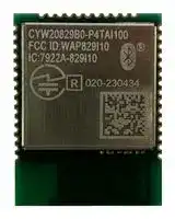


CYW20829B0P4TAI100XUMA1
Bluetooth Module, BLE 5.4, 2 Mbps, -106 dBm, 2.75 to 3.6 V, -30 °C to 85 °C, AIROC Series
- Manufacturer: INFINEON
- Product type: Bluetooth Modules & Adaptors
- SVHC: No SVHC (25-Jun-2025)
- Interfaces: I2C, SPI, UART
- Product Range: AIROC Series
- Certifications: CE, FCC, ISED, MIC
- Bluetooth Class: Class 1, Class 2
- Bluetooth Version: Bluetooth LE 5.4
- Supply Voltage Range: 2.75 V to 3.6 V
- Receiver Sensitivity Rx: -106 dBm
- Operating Temperature Range: -30 °C to 85 °C
| Delivery and price | |
|---|---|
| Units per pack | 250 |
| Price | 3.93 € |
| Current stock | 500+ |
| Lead time | 30 days |
## **CYW20829B0-P4TAI100, CYW20829B0-P4EPI100** A/™ **AIROC™ Bluetooth® LE module** ## **General description** The CYW20829B0-P4TAI100 is a fully integrated Bluetooth® LE wireless module. The CYW20829B0-P4TAI100 includes an onboard crystal oscillator, passive components, flash memory, and the CYW20829 silicon device. Refer to the **CYW20829** datasheet for additional details on the capabilities of the silicon device used in this module. The CYW20829B0-P4TAI100 supports high-performance analog-to-digital conversion audio input, I[2] S/PCM, CAN, LIN for automotive use cases and other standard communication and timing peripherals. The CYW20829B0-P4TAI100 includes a royalty-free Bluetooth® stack compatible with Bluetooth® 5.4 core spec in a 14.5 × 19 × 1.95 mm package. The CYW20829B0-P4TAI100 includes 1 MB of onboard serial flash memory and is designed for standalone operation. The CYW20829B0-P4TAI100 uses an integrated power amplifier to achieve Class I or Class II output power capability. The CYW20829B0-P4TAI100 is fully qualified by Bluetooth® SIG and is targeted at applications requiring cost-optimized Bluetooth® wireless connectivity. The CYW20829B0-P4TAI100 is offered in two certified versions CYW20829B0-P4TAI100, and CYW20829B0-P4EPI100. The CYW20829B0-P4TAI100 includes an integrated trace antenna. The CYW20829B0-P4EPI100 supports an external antenna through a RF solder pad output. ## **Module description** - Module size: 14.5 × 19 × 1.95 mm - Bluetooth® 5.4 core spec qualified module - QDID: TBD - Declaration ID: TBD - Certified to FCC, ISED, MIC, and CE regulations - Castelated solder pad connections for ease-of-use - 1-MB on-module serial flash memory - Up to 26 GPIOs - Temperature range: –30°C to +85°C - 96-MHz Arm® Cortex®-M33 CPU with single-cycle multiply and memory protection unit (MPU) - Maximum TX output power - Programmable TX power: up to 10 dBm - Bluetooth® LE connection range of up to 500 meters at 10 dBm[[1]] - RX sensitivity: - LE-1 Mbps: –98 dBm - LE-2 Mbps: –95 dBm - Coded PHY 500 kbps (LE-LR): –101 dBm - Coded PHY 125 kbps (LE-LR): –106 dBm ## **Note** 1. Connection range tested module-to-module using Bluetooth® Low Energy Long Range Coded PHY technology in full line-of-sight environment, free of obstacles or interference sources with output power of +10.0 dBm. Actual range will vary based on end product design, environment, receive sensitivity, and transmit output power of the central device. Please read the Important Notice and Warnings at the end of this document page 1 Datasheet www.infineon.com 002-39262 Rev. ** 2024-01-23 **AIROC™ Bluetooth® LE module** Power consumption ## **Power consumption** - Bluetooth® LE current consumption - RX current: 5.6 mA @ LE 1 Mbps - TX current: 5.2 mA @ 0 dBm - Deep Sleep mode current with 64 KB SRAM retention: 4.5 µA - HIDOFF (Deep Sleep): 0.5 µA ## **Functional capabilities** - Flexible clocking options - 8-MHz internal main oscillator (IMO) with ±2% accuracy - Ultra-low-power 32-kHz internal low-speed oscillator (ILO) - Two oscillators: High-frequency (24-MHz) for radio PLL and low-frequency (32-kHz watch crystal) for LPO - 48-MHz low power IHO (internal oscillator) - Frequency-locked loop (FLL) for multiplying IMO frequency - Integer and fractional peripheral clock dividers - Quad SPI (QSPI)/serial memory interface (SMIF) - eXecute-In-Place (XIP) from external quad SPI flash - On-the-fly encryption and decryption - Support for DDR - Supports single, dual, and quad interfaces with throughput up to 384-Mbps - Serial Communication - Three run-time configurable Serial Communication Blocks (SCBs) - First SCB: Configurable as SPI or I[2] C - Second SCB: Configurable as SPI or UART - Third SCB: Configurable as I[2] C or UART - Audio subsystem - Two pulse density modulation (PDM) channels and one I2 S channel with time division multiplexed (TDM) mode - Timing and pulse-width modulation - Seven 16-bit and two 32-bit Timer/Counter Pulse-Width Modulator (TCPWM) blocks, for MCU. Multiple PWMs needed for color LEDs. - PWM supports center-aligned, edge, and pseudo-random modes - ADC and MIC - Sigma-delta switched cap ADC for audio and DC measurements - Up to 32 programmable GPIOs - One I/O port (8 I/Os) enables Boolean operations on GPIO pins; available during system Deep Sleep - Programmable drive modes, strengths, and slew rates - Two overvoltage-tolerant (OVT) pins - Up to six, used for SMIF Datasheet 002-39262 Rev. ** 2 2024-01-23 ## **AIROC™ Bluetooth® LE module** ## Benefits - Security built into platform architecture - ROM-based root of trust via uninterruptible “Secure Boot” - Step-wise authentication of execution images - Secure execution of code in execute-only mode for protected routines - All debug and test ingress paths can be disabled - Up to four protection contexts (One available for customer code) - Secure debug support via authenticated debug token - Encrypted image support for external SMIF memory - Cryptography hardware - Hardware Acceleration for symmetric cryptographic methods and hash functions - True Random Number Generation (TRNG) function ## **Benefits** CYW20829B0-P4TAI100 provides all necessary components required to operate Bluetooth® LE communication standards. - Proven ready-to-use hardware design - Cost optimized for applications without space constraints - Nonvolatile memory for self-sufficient operation and over-the-air updates - Bluetooth® SIG listed with QDID and declaration ID - Fully certified module eliminates the time needed for design, development, and certification processes - ModusToolbox™ provides an easy-to-use integrated design environment (IDE) to configure, develop, and program a Bluetooth® application Datasheet 002-39262 Rev. ** 3 2024-01-23 **AIROC™ Bluetooth® LE module** More information ## **More information** Infineon provides a wealth of data at **www.infineon.com** to help you to select the right module for your design, and to help you to quickly and effectively integrate the module into your design. ## **References** - Overview: **AIROC™ Bluetooth® LE & Bluetooth® portfolio** , **Module portfolio** - **CYW20829 Bluetooth® silicon datasheet** - Development kits: - **CYW920829B0M2P4TAI100-EVK** , CYW20829B0-P4TAI100 evaluation board - **CYW920829B0M2P4EPI100-EVK** , CYW20829B0-P4EPI100 evaluation board - Test and debug tools: - **CYSmart** , Bluetooth® LE test and debug tool (Windows) - **CYSmart Mobile** , Bluetooth® LE test and debug tool (Android/iOS Mobile App) - Knowledge base article - **KBA97095** - EZ-Bluetooth® LE module placement - **KBA213976** - FAQ for Bluetooth® LE and regulatory certifications with EZ-BLE modules - **KBA210802** - Queries on Bluetooth® LE qualification and declaration processes - **KBA218122** - 3D Model Files for EZ-BLE/EZ-BT modules ## **Development environments** ModusToolbox™ software is a modern, extensible development environment supporting a wide range of Infineon microcontroller devices. It provides a flexible set of tools and a diverse, high-quality collection of application-focused software. These include configuration tools, low-level drivers, libraries, and operating system support, most of which are compatible with Linux®, macOS®, and Windows®-hosted environments. ModusToolbox™ software does not include proprietary tools or custom build environments. This means you choose your compiler, your IDE, your RTOS, and your ecosystem without compromising usability or access to our industry leading CAPSENSE™, AIROC™, Bluetooth®, Wi-Fi, security, and low-power features. ## **Technical support** - **Infineon community:** Whether you are a customer, partner, or a developer interested in the latest innovations, the developer community offers you a place to learn, share, and engage with both Infineon experts and other embedded engineers around the world. - Visit our **support** page and contact a **local sales representatives** . If you are in the United States, you can talk to our technical support team by calling our toll-free number: +1-800-541-4736. Select option 2 at the prompt. Datasheet 002-39262 Rev. ** 4 2024-01-23 ## **AIROC™ Bluetooth® LE module** Table of contents ## **Table of contents** **General description ...........................................................................................................................1 Module description............................................................................................................................1 Power consumption...........................................................................................................................2 Functional capabilities.......................................................................................................................2 Benefits............................................................................................................................................3 More information ..............................................................................................................................4 References........................................................................................................................................4 Development environments...............................................................................................................4 Technical support..............................................................................................................................4 Table of contents...............................................................................................................................5 1 Overview .......................................................................................................................................7** 1.1 Functional block diagram.......................................................................................................................................7 1.2 Module description.................................................................................................................................................7 1.2.1 Module dimensions and drawing........................................................................................................................7 **2 Pad connection interface.................................................................................................................9 3 Recommended host PCB layout......................................................................................................11 4 Module connections ......................................................................................................................12 5 Connections and optional external components..............................................................................16** 5.1 Power connections (VBAT).....................................................................................................................................16 5.1.1 Considerations and optional components for Brown Out (BO) conditions....................................................16 5.2 External reset (XRES) ............................................................................................................................................17 5.3 Critical components list........................................................................................................................................19 5.4 Antenna design .....................................................................................................................................................19 **6 Functional description ..................................................................................................................20** 6.1 CPU and memory subsystem ...............................................................................................................................20 6.1.1 CPU .....................................................................................................................................................................21 6.1.2 Interrupts............................................................................................................................................................21 6.1.3 Datawire .............................................................................................................................................................21 6.1.4 Cryptography accelerator (Cryptolite)..............................................................................................................22 6.1.5 Protection units .................................................................................................................................................22 6.1.6 AES-128...............................................................................................................................................................22 6.1.7 Vector unit (VU) ..................................................................................................................................................22 6.1.8 Controller area network flexible data-rate (CAN FD) .......................................................................................22 6.1.9 Local interconnect network (LIN) .....................................................................................................................23 6.1.10 Real time clock (RTC).......................................................................................................................................23 6.1.11 Memory.............................................................................................................................................................23 6.1.12 Boot code .........................................................................................................................................................23 6.1.13 Memory map ....................................................................................................................................................24 **7 System resources..........................................................................................................................25** 7.1 Power system........................................................................................................................................................25 7.1.1 Power modes .....................................................................................................................................................25 7.1.2 CYW20829 clock system.....................................................................................................................................26 7.1.3 Internal main oscillator (IMO) ...........................................................................................................................27 7.1.4 Internal low-speed oscillator (ILO) ...................................................................................................................27 7.1.5 External crystal oscillators (ECO)......................................................................................................................28 7.1.6 Watchdog timers (WDT, MCWDT)......................................................................................................................28 7.1.7 Clock dividers.....................................................................................................................................................28 7.1.8 Trigger routing ...................................................................................................................................................28 7.1.9 Reset...................................................................................................................................................................29 7.2 Bluetooth® LE radio and subsystem ....................................................................................................................30 7.3 Programmable analog-to-digital converter (ADC)..............................................................................................30 Datasheet 002-39262 Rev. ** 5 2024-01-23 ## **AIROC™ Bluetooth® LE module** ## Table of contents 7.3.1 Sigma delta ADC.................................................................................................................................................30 7.4 Programmable digital...........................................................................................................................................30 7.5 Fixed-function digital............................................................................................................................................31 7.5.1 Timer/counter/pulse-width modulator (TCPWM) block..................................................................................31 7.5.2 Serial communication blocks (SCB)..................................................................................................................32 7.5.3 QSPI interface serial memory interface (SMIF).................................................................................................32 7.6 GPIO.......................................................................................................................................................................33 7.7 Special-function peripherals................................................................................................................................34 7.7.1 Audio subsystem................................................................................................................................................34 **8 Electrical characteristics ...............................................................................................................35** 8.1 Absolute maximum ratings ..................................................................................................................................35 8.2 Operating conditions............................................................................................................................................36 8.2.1 XRES....................................................................................................................................................................38 8.2.2 GPIO....................................................................................................................................................................39 8.3 Analog peripherals................................................................................................................................................41 8.3.1 AUD ADC .............................................................................................................................................................41 8.4 Digital peripherals.................................................................................................................................................43 8.5 Audio subsystem...................................................................................................................................................46 8.6 System resources..................................................................................................................................................51 8.6.1 Power-on reset...................................................................................................................................................51 8.6.2 Voltage monitors................................................................................................................................................52 8.6.3 SWD and trace interface ....................................................................................................................................53 8.6.4 Internal main oscillator .....................................................................................................................................53 8.6.5 Internal low-speed oscillator ............................................................................................................................54 8.6.6 FLL ......................................................................................................................................................................54 8.6.7 Crystal oscillator ................................................................................................................................................55 8.6.8 Clock source switching time..............................................................................................................................55 8.6.9 QSPI ....................................................................................................................................................................56 8.6.10 Smart I/O ..........................................................................................................................................................56 8.6.11 JTAG boundary scan........................................................................................................................................57 8.7 Bluetooth® LE........................................................................................................................................................58 **9 Environmental specifications ........................................................................................................66** 9.1 Environmental compliance..................................................................................................................................66 9.2 RF certification......................................................................................................................................................66 9.3 Safety certification................................................................................................................................................66 9.4 Environmental conditions....................................................................................................................................66 9.5 ESD and EMI protection........................................................................................................................................66 **10 Regulatory information ...............................................................................................................67** 10.1 FCC.......................................................................................................................................................................67 10.2 ISED......................................................................................................................................................................68 10.3 European declaration of conformity..................................................................................................................69 10.4 MIC Japan............................................................................................................................................................70 **11 Packaging ..................................................................................................................................71 12 Ordering information ..................................................................................................................73 13 Acronyms ...................................................................................................................................74 14 Document conventions................................................................................................................78** 14.1 Units of measure.................................................................................................................................................78 **Revision history ..............................................................................................................................79** Datasheet 002-39262 Rev. ** 6 2024-01-23 **AIROC™ Bluetooth® LE module** Overview ## **1 Overview** ## **1.1 Functional block diagram** **Figure 1** illustrates the CYW20829B0-P4TAI100 functional block diagram. **==> picture [337 x 178] intentionally omitted <==** **----- Start of picture text -----**<br> XRES<br>Up to 2<br>SCBs<br>(I2C, SPI,<br>UART)<br>SCB CYW20829<br>Deep Silicon Device<br>Sleep<br>(I2C, SPI)<br>CAN-FD<br>ADC<br>UP to 9<br>TCPWMs Passive Components 1 MB 24 MHz<br>(RES, CAP, IND) SERIAL FLASH XTAL<br>Up to 26 GPIOs<br>**----- End of picture text -----**<br> ## **Figure 1 Functional block diagram (GPIOs)** ## **1.2 Module description** The CYW20829B0-P4TAI100 module is a complete module designed to be soldered to the application’s main board. ## **1.2.1 Module dimensions and drawing** Infineon reserves the right to select components from various vendors to achieve the Bluetooth® module functionality. Such selections will still guarantee that all mechanical specifications and module certifications are maintained. Designs should be held within the physical dimensions shown in the mechanical drawings in **Figure 2** . All dimensions are in millimeters (mm). ## **Table 1 Module design dimensions** |**Table 1**<br>**Module design dimensions**|**Table 1**<br>**Module design dimensions**|| |---|---|---| |**Dimension item**||**Specification**| |Module dimensions|Length (X)<br>~~OS~~|14.5 ± 0.15 mm| ||Width (Y)<br>~~OS~~|19 ± 0.15 mm| |Antenna connection location dimensions|Length (X)<br>~~I~~|14.5 mm| ||Width (Y)<br>~~OS~~|4.62 mm| |PCB thickness|Height (H)<br>~~OS~~|0.50 ± 0.05 mm| |Shield height|Height (H)<br>~~Oy~~|1.45-mm typical| |Maximum component height|Height (H)<br>~~—~~|1.45-mm typical| |Total module thickness (bottom of module to highest<br>component)|Height (H)<br>~~oe~~|1.95-mm typical| Datasheet 002-39262 Rev. ** 7 2024-01-23 **AIROC™ Bluetooth® LE module** ## Overview See **Figure 2** for the mechanical reference drawing for CYW20829B0-P4TAI100. **Figure 2 Module mechanical drawing** ## **Notes** 2. No metal should be located beneath or above the antenna area. Only bare PCB material should be located beneath the antenna area. For more information on recommended host PCB layout, see **“Recommended host PCB layout”** on page 11. 3. The CYW20829B0-P4TAI100, CYW20829B0-P4EPI100 includes castellated pad connections, denoted as the circular openings at the pad location above. Datasheet 002-39262 Rev. ** 2024-01-23 8 **AIROC™ Bluetooth® LE module** Pad connection interface ## **2 Pad connection interface** As shown in the bottom view of **Figure 2** , the CYW20829B0-P4TAI100 connects to the host board via solder pads on the backside of the module. **Table 2** and **Figure 3** detail the solder pad length, width, and pitch dimensions of the CYW20829B0-P4TAI100 module. **Table 2 Connection description** |**Part number**|**Name **|**Connections**|**Connection type**|**Pad length**<br>**dimension**|**Pad width**<br>**dimension**|**Pad pitch**| |---|---|---|---|---|---|---| |CYW20829B0-P4TAI100|SP|41|Solder pads|1.02 mm|0.61 mm|0.90 mm| |CYW20829B0-P4EPI100|SP|41|Solder pads|1.02 mm|0.61 mm|0.90 mm| ## **Figure 3 Solder pad dimensions (seen from bottom)** To maximize RF performance, the host layout should follow these recommendations: 1. Antenna Area Keepout: The host board directly below the antenna area of the module (see **Figure 2** ) must not contain ground or signal traces. This keepout area requirement applies to all layers of the host board. 2. Module Placement: The ideal placement of the Bluetooth® module is in a corner of the host board with the PCB trace antenna located at the far corner. This placement minimizes the additional recommended keepout area stated in item 2. Refer to **AN96841** for module placement best practices. Datasheet 002-39262 Rev. ** 9 2024-01-23 **AIROC™ Bluetooth® LE module** Pad connection interface **Figure 4 Recommended host PCB keepout area around the CYW20829B0-P4TAI100 antenna** Datasheet 002-39262 Rev. ** 10 2024-01-23 **AIROC™ Bluetooth® LE module** Recommended host PCB layout ## **3 Recommended host PCB layout** **Figure 5** provides details that can be used for the recommended host PCB layout pattern for the CYW20829B0-P4TAI100. Dimensions are in millimeters unless otherwise noted. Pad length of 1.27 mm (0.64 mm from center of the pad on either side) shown in **Figure 4** is the minimum recommended host pad length. The host PCB layout pattern can be completed using either **Figure 5** . It is not necessary to use all figures to complete the host PCB layout pattern. **Figure 5 CYW20829B0-P4TAI100 host layout (dimensioned)** Datasheet 002-39262 Rev. ** 2024-01-23 11 **AIROC™ Bluetooth® LE module** Module connections ## **4 Module connections** **Table 3** details the solder pad connection definitions and available functions for the pad connections for the CYW20829B0-P4TAI100 module. **Table 3** lists the solder pads on the CYW20829B0-P4TAI100 module, the silicon device pin, and denotes what functions are available for each solder pad. |**Module pad name**<br>~~Ss~~|**Pin**<br>**number **<br>~~ff~~<br>~~Ss~~|**Silicon pin name**<br>~~ff~~|**Pin**<br>**number **<br>~~ff~~|**I/O**<br>~~ff~~|**Power**<br>**domain**<br>~~ff~~|**Description**| |---|---|---|---|---|---|---| |**Microphone**<br>~~Ss~~|~~ff~~<br>~~Ss~~|**Microphone**<br>~~ff~~|~~ff~~|~~ff~~|~~ff~~|| |MIC_P<br>~~Ss~~|24<br>~~Ss~~<br>~~ee~~|MIC_P<br>~~ee~~|54<br>~~ee~~|I<br>|VDDA<br>|Microphone positive input| |MIC_N|25<br>~~ee~~<br>~~es~~|MIC_N<br>~~ee~~<br>|55<br>~~ee~~<br>|||Microphone negative input| |MIC_BIAS|23<br>~~ee~~<br>~~es~~|MIC_BIAS<br>~~ee~~<br>|53<br>~~ee~~<br>|O<br>||Microphone bias supply| |GND_A<br>~~Ss~~|22, 26<br>~~es|~~<br>~~Ss~~|~~|~~|~~|~~|~~|~~|~~|~~|Analog ground for<br>microphone| |~~Ss~~<br>~~Ss~~|~~|~~<br>~~Ss~~<br>~~Ss~~|~~|~~|~~|~~|~~|~~|~~|~~|| |**Power supply**<br>~~Ss~~<br>~~Ss~~<br>~~Ss~~|~~Ss~~<br>~~Ss~~<br>~~Ss~~|||||| |VBAT<br>~~Ss~~<br>~~Ss~~<br>~~Ss~~|15<br>~~Ss~~<br>~~Ss~~<br>~~Ss~~|2.75 V~3.6 V<br>||||| |~~Ss~~<br>~~Ss~~|~~Ss~~<br>~~Ss~~|||||| |**Ground pins**<br>~~Ss~~|~~Ss>>~~|~~>>~~|~~>>~~|~~>>~~|~~>>~~|| |GND<br><br>~~Ss~~|1, 2, 14,<br>21, 33,<br>39, 41<br>~~>>~~<br>~~Ss~~|~~>>~~|~~>>~~|~~>>~~|~~>>~~|| |~~Ss~~<br>~~Ss~~|~~Ss~~<br>~~Ss~~|||||| |**Radio I/O**<br>~~Ss~~<br>~~Ss~~<br>~~Ss~~|~~Ss~~<br>~~Ss~~<br>~~Ss~~|||~~eee~~|~~eee~~|~~eee~~| |RFIO<br>~~Ss~~<br>~~Ss~~|40<br>~~Ssee~~<br>~~Ss~~|~~ee~~|~~ee~~|I/O<br>~~ee~~<br>~~eee~~|~~ee~~<br>~~eee~~|External antenna port (only<br>for CYW20829B0-P4EPI100)<br>~~eee~~| |~~Ss~~|~~Ss~~|||~~eee~~|~~eee~~|~~eee~~| Datasheet 002-39262 Rev. ** 12 2024-01-23 **AIROC™ Bluetooth® LE module** ## Module connections |**Module**<br>**pad name**|**Pad**<br>**number**<br>~~es~~|**Silicon**<br>**pin name**|**Silicon**<br>**pin**<br>**number**|**Direction**<br>**Default**|**POR state **|**Power**<br>**domain**|**Description**| |---|---|---|---|---|---|---|---| |P0.0|6<br>~~es~~<br>~~es~~|P0.0<br>~~es~~|32<br>~~es~~|I/O<br>~~es~~|Floating<br>~~es~~|VDDO<br>~~es~~|General input and output<br>port.<br>See**Table 5**for alternate<br>functions.| |P0.1|7<br>~~es~~<br>~~es~~<br>~~es~~|P0.1<br>~~es~~|33<br>~~es~~|I/O<br>~~es~~|Floating<br>~~es~~|VDDO<br>~~es~~|| |P0.2|8<br>~~es~~<br>~~es~~<br>~~es~~|P0.2<br>~~es~~<br>~~es~~|34<br>~~es~~<br>~~es~~|I/O<br>~~es~~|Floating<br>~~es~~|VDDO<br>~~es~~|| |P0.3|9<br>~~es~~<br>~~es~~<br>~~es~~|P0.3<br>~~es~~<br>~~es~~|35<br>~~es~~<br>~~es~~|I/O<br>~~es~~|Floating<br>~~es~~|VDDO<br>~~es~~|| |P0.4|10<br>~~es~~<br>~~es~~<br>~~es~~|P0.4<br>~~es~~<br>~~es~~<br>~~es~~|36<br>~~es~~<br>~~es~~<br>~~es~~|I/O<br>~~es~~<br>~~es~~|Floating<br>~~es~~<br>~~es~~|VDDO<br>~~es~~<br>~~es~~|| |P0.5|11<br>~~es~~<br>~~es~~<br>~~es~~|P0.5<br>~~es~~<br>~~es~~|37<br>~~es~~<br>~~es~~|I/O<br>~~es~~<br>~~es~~|Floating<br>~~es~~<br>~~es~~|VDDO<br>~~es~~<br>~~es~~|| |P1.0|4<br>~~es~~<br>~~es~~<br>~~es~~|P1.0<br>~~es~~<br>~~es~~|38<br>~~es~~<br>~~es~~|I/O<br>~~es~~|Floating<br>~~es~~|VDDO<br>~~es~~|| |P1.1|5<br>~~es~~<br>~~es~~<br>~~es~~|P1.1<br>~~es~~<br>~~es~~|39<br>~~es~~<br>~~es~~|I/O<br>~~es~~|Floating<br>~~es~~|VDDO<br>~~es~~|| |P1.2|12<br>~~es~~<br>~~es~~<br>~~es~~|P1.2<br>~~es~~<br>~~es~~<br>~~es~~|40<br>~~es~~<br>~~es~~<br>~~es~~|I/O<br>~~es~~<br>~~es~~|Floating<br>~~es~~<br>~~es~~|VDDO<br>~~es~~<br>~~es~~|| |P1.3|13<br>~~es~~<br>~~es~~<br>~~es~~|P1.3<br>~~es~~<br>~~es~~|41<br>~~es~~<br>~~es~~|I/O<br>~~es~~<br>~~es~~|Floating<br>~~es~~<br>~~es~~|VDDO<br>~~es~~<br>~~es~~|| |P1.4|18<br>~~es~~<br>~~es~~<br>~~es~~|P1.4<br>~~es~~<br>~~es~~|43<br>~~es~~<br>~~es~~|I/O<br>~~es~~|Floating<br>~~es~~|VDDO<br>~~es~~|| |P1.5|19<br>~~es~~<br>~~es~~<br>~~es~~|P1.5<br>~~es~~<br>~~es~~|44<br>~~es~~<br>~~es~~|I/O<br>~~es~~|Floating<br>~~es~~|VDDO<br>~~es~~|| |P1.6|20<br>~~es~~<br>~~es~~<br>~~es~~|P1.6<br>~~es~~<br>~~es~~<br>~~es~~|45<br>~~es~~<br>~~es~~<br>~~es~~|I/O<br>~~es~~<br>~~es~~|Floating<br>~~es~~<br>~~es~~|VDDO<br>~~es~~<br>~~es~~|| |P3.0|27<br>~~es~~<br>~~es~~<br>~~es~~|P3.0<br>~~es~~<br>~~es~~|1<br>~~es~~<br>~~es~~|I/O<br>~~es~~<br>~~es~~|Floating<br>~~es~~<br>~~es~~|VDDO<br>~~es~~<br>~~es~~|| |P3.1|28<br>~~es~~<br>~~es~~<br>~~es~~|P3.1<br>~~es~~<br>~~es~~|2<br>~~es~~<br>~~es~~|I/O<br>~~es~~|Floating<br>~~es~~|VDDO<br>~~es~~|| |P3.2|29<br>~~es~~<br>~~es~~<br>~~es~~|P3.2<br>~~es~~<br>~~es~~|3<br>~~es~~<br>~~es~~|I/O<br>~~es~~|Floating<br>~~es~~|VDDO<br>~~es~~|| |P3.3|30<br>~~es~~<br>~~es~~<br>~~es~~|P3.3<br>~~es~~<br>~~es~~<br>~~es~~|4<br>~~es~~<br>~~es~~<br>~~es~~|I/O<br>~~es~~<br>~~es~~|Floating<br>~~es~~<br>~~es~~|VDDO<br>~~es~~<br>~~es~~|| |P3.4|16<br>~~es~~<br>~~es~~<br>~~es~~|P3.4<br>~~es~~<br>~~es~~|5<br>~~es~~<br>~~es~~|I/O<br>~~es~~<br>~~es~~|Floating<br>~~es~~<br>~~es~~|VDDO<br>~~es~~<br>~~es~~|| |P3.5|17<br>~~es~~<br>~~es~~<br>~~es~~|P3.5<br>~~es~~<br>~~es~~|6<br>~~es~~<br>~~es~~|I/O<br>~~es~~|Floating<br>~~es~~|VDDO<br>~~es~~|| |P3.6|31<br>~~es~~<br>~~es~~<br>~~es~~|P3.6<br>~~es~~<br>~~es~~|8<br>~~es~~<br>~~es~~|I/O<br>~~es~~|Floating<br>~~es~~|VDDO<br>~~es~~|| |P3.7|32<br>~~es~~<br>~~es~~<br>~~es~~|P3.7<br>~~es~~<br>~~es~~<br>~~es~~|9<br>~~es~~<br>~~es~~<br>~~es~~|I/O<br>~~es~~<br>~~es~~|Floating<br>~~es~~<br>~~es~~|VDDO<br>~~es~~<br>~~es~~|| |P4.0|37<br>~~es~~<br>~~es~~<br>~~es~~|P4.0<br>~~es~~<br>~~es~~<br>|13<br>~~es~~<br>~~es~~<br>|I/O<br>~~es~~<br>~~es~~<br>|Floating<br>~~es~~<br>~~es~~<br>|VDDO<br>~~es~~<br>~~es~~<br>|| |P4.1|38<br>~~es~~<br>~~es~~|P4.1<br>~~es~~<br>|14<br>~~es~~<br>|I/O<br>~~es~~<br>|Floating<br>~~es~~<br>|VDDO<br>~~es~~<br>|| |P5.0/<br>WCO_OUT|34<br>~~esfff~~<br>~~|~~|P5.0/<br>WCO_OUT <br>~~fff~~<br>~~fF~~|10<br>~~fff~~<br>~~fF~~<br>~~fF~~|I/O<br>~~fff~~<br>~~fF~~|Floating<br>~~fff~~<br>|VDDO<br>~~fff~~<br>|| |P5.1/<br>WCO_IN|35<br>~~fff~~<br>~~|~~<br>~~es~~|P5.1/<br>WCO_IN<br>~~fff~~<br>~~fF~~<br>|11<br>~~fff~~<br>~~fF~~<br>~~fF~~<br>|I/O<br>~~fff~~<br>~~fFff~~<br>|Floating<br>~~fff~~<br>~~ff~~<br>|VDDO<br>~~fff~~<br>~~ff~~<br>|| |P5.2|36<br>~~|~~<br>~~es~~<br>~~es~~|P5.2<br>~~fF~~<br>~~es~~<br>~~es~~|12<br>~~fF~~<br>~~fF~~<br>~~es~~<br>~~es~~|~~fFff~~<br>~~es~~|Floating<br>~~ff~~<br>~~es~~|VDDO<br>~~ff~~<br>~~es~~|| |XRES|3<br>~~es~~<br>~~es~~|XRES<br>~~es~~<br>~~es~~|23<br><br>~~es~~<br>~~es~~|I<br>~~ff~~<br>~~es~~|Floating<br>~~ff~~<br>~~es~~|VDDO<br>~~ff~~<br>~~es~~|| ## **Notes** 4. The CYW20829B0-P4TAI100 contains a single SPI (SPI1) peripheral supporting both master or slave configurations. SPI2 is used for on-module serial memory interface. 5. In Master mode, any available GPIO can be configured as SPI1_CS. Datasheet 002-39262 Rev. ** 13 2024-01-23 ## Each port pin has multiple alternate functions. These are defined in **Table 5** . |**Port/Pin**|**Analog**<br>~~PTT~~|**ACT #0**<br>~~PTT~~|**ACT #1**<br>~~PTTTTP~~|**ACT #4**<br>~~TTP~~|**ACT #5**<br>~~TTP~~|**ACT #6**<br>~~TTPPr~~|**ACT #7**<br>~~Pr~~|**ACT #8**<br>~~Prrrr~~|**ACT #9**<br>~~rrr~~|**ACT #10**<br>~~rrr~~|**ACT #11**<br>~~rrrPr~~|**ACT #12**<br>~~Pr~~|**ACT #13**<br>~~Pr~~|**ACT #14**<br>~~rr~~|**ACT #15**<br>~~rr~~|**DS #2**<br>~~rr~~|**DS #3**|**DS #5**|**DS #6**|**DS #7**| |---|---|---|---|---|---|---|---|---|---|---|---|---|---|---|---|---|---|---|---|---| |P0.0<br>~~Ss~~|~~PTT~~<br>~~Ss~~|tcpwm[0].<br>line_<br>compl[0]:3<br>~~PTT~~<br>~~es~~|tcpwm[0].<br>line_<br>compl[262]:0<br>~~PTTTTP~~<br>~~es~~|~~TTP~~<br>~~OO~~|~~TTP~~<br>~~OO~~|~~TTPPr~~<br>|~~Pr~~<br>~~On~~|~~Prrrr~~<br>~~On~~|pdm.<br>pdm_<br>clk[1]:0<br>~~rrr~~<br>~~OO~~|~~rrr~~<br>~~OO~~|~~rrrPr~~<br>|tdm.tdm_<br>tx_<br>mck[0]:0<br>~~Pr~~<br>~~OO~~|tdm.tdm_<br>rx_<br>mck[0]:0<br>~~Pr~~<br>~~OO~~|~~rr~~<br>~~OO~~|~~rr~~|keyscan.<br>ks_<br>col[2]<br>~~rr~~|||scb[0].<br>spi_<br>select1:0|| |P0.1<br>~~Ss~~|~~PTT~~<br>~~Ss~~<br>~~PT~~|tcpwm[0].<br>line[1]:3<br>~~PTT~~<br>~~es~~<br>~~PT~~|tcpwm[0].<br>line[256]:1<br>~~PTT TTP~~<br>~~es~~<br>~~TTP~~|~~TTP~~<br>~~OO~~<br>~~TTP~~|~~TTP~~<br>~~OO~~<br>~~TTP~~|~~TTP Pr~~<br><br>~~TTPPr~~|~~Pr~~<br>~~On~~<br>~~Pr~~|~~Pr rrr~~<br>~~On~~<br>~~Pryr~~|pdm.<br>pdm_<br>data[1]:0<br>~~rrr~~<br>~~OO~~<br>~~yr~~|~~rrr~~<br>~~OO~~<br>~~yr~~|~~rrr Pr~~<br><br>~~Pr~~|tdm.tdm_<br>tx_sck[0]:0<br>~~Pr~~<br>~~OO~~<br>~~Pr~~|~~Pr ~~<br>~~OO~~<br>~~Prrr~~|~~rr~~<br>~~OO~~<br>~~rr~~|~~rr~~<br>~~rr~~|keyscan.<br>ks_<br>col[3]<br>~~rr~~|||scb[0].<br>spi_<br>select2:0|| |P0.2<br>~~Ss~~|~~Ss ~~<br>~~PT~~<br>~~PT~~|tcpwm[0].<br>line_<br>compl[1]:3<br> ~~es~~<br>~~PT~~<br>~~PT~~|tcpwm[0].<br>line_<br>compl[256]:1<br>~~es~~<br>~~TTP~~<br>~~TTP~~|~~OO~~<br>~~TTP~~<br>~~TTP~~|~~OO ~~<br>~~TTP~~<br>~~TTP~~|<br>~~TTPPr~~<br>~~TTPPr~~|~~On~~<br>~~Pr~~<br>~~Pr~~|~~On~~<br>~~Pryr~~<br>~~Pryr~~|~~OO~~<br>~~yr~~<br>~~yr~~|peri.tr_io_<br>input[4]:0<br>~~OO ~~<br>~~yr~~<br>~~yr~~|<br>~~Pr~~<br>~~Pr~~|tdm.tdm_<br>tx_<br>fsync[0]:0<br> ~~OO~~<br>~~Pr~~<br>~~Pr~~|~~OO~~<br>~~Prrr~~<br>~~Prrr~~|~~OO~~<br>~~rr~~<br>~~rr~~|~~rr~~<br>~~rr~~|keyscan.<br>ks_<br>col[11]|scb[0].<br>i2c_scl:0||scb[0].<br>spi_<br>mosi:0|| |P0.3|~~PT~~<br>~~PT~~<br>~~PTT~~|tcpwm[0].<br>line[0]:4<br>~~PT ~~<br>~~PT~~<br>~~PTT~~|tcpwm[0].<br>line[257]:1<br> ~~TTP~~<br>~~TTP~~<br>~~PTT~~|~~TTP~~<br>~~TTP~~<br>|~~TTP~~<br>~~TTP~~<br>|~~TTP Pr~~<br>~~TTPPr~~<br>|~~Pr~~<br>~~Pr~~<br>~~OO~~<br>|scb[1].spi_<br>select3:0<br>~~Pr yr~~<br>~~Pryr~~<br>~~OO~~<br>|~~yr~~<br>~~yr~~<br>~~OO~~<br>|~~yr~~<br>~~yr~~<br>~~OO~~<br>|~~Pr~~<br>~~Pr~~<br>~~OO~~<br>|tdm.tdm_<br>tx_sd[0]:0<br>~~Pr~~<br>~~Pr~~<br>~~OO~~<br>|~~Pr rr~~<br>~~Prrr~~<br>~~OO~~<br>|~~rr~~<br>~~rr~~<br>~~OO~~<br>|~~rr~~<br>~~rr~~<br>|keyscan.<br>ks_<br>col[12]|scb[0].<br>i2c_sda:0||scb[0].<br>spi_<br>miso:0|| |P0.4|~~PT~~<br>~~OO~~<br>~~PTT~~<br>~~pit~~|tcpwm[0].<br>line_<br>compl[0]:4<br>~~PT ~~<br>~~OO~~<br>~~PTT~~<br>~~pit~~|tcpwm[0].<br>line_<br>compl[257]:1<br> ~~TTP~~<br>~~OO~~<br>~~PTT TTP~~<br>~~pit~~|srss.ext_<br>clk:0<br>~~TTP~~<br>~~OO~~<br>~~TTP~~<br>|cpuss.<br>trace_<br>data[3]:1<br>~~TTP~~<br>~~OO~~<br>~~TTP~~<br>|~~TTP Pr~~<br>~~OO~~<br>~~TTPPr~~<br>|~~Pr~~<br>~~OO~~<br>~~OO~~<br>~~Pr~~<br>|scb[1].spi_<br>select2:0<br>~~Pr yr~~<br>~~OO~~<br>~~OO~~<br>~~Prrr~~<br>|~~yr~~<br>~~OO~~<br>~~OO~~<br>~~rr~~<br>|peri.tr_io_<br>input[0]:0<br>~~yr~~<br>~~OO~~<br>~~OO~~<br>~~rr~~<br>|~~Pr~~<br>~~OO~~<br>~~OO~~<br>~~Pr~~<br>|tdm.tdm_<br>rx_sck[0]:0<br>~~Pr~~<br>~~OO~~<br>~~OO~~<br>~~Pr~~<br>|~~Pr rr~~<br>~~OO~~<br>~~OO~~<br>~~Prrr~~|~~rr~~<br>~~OO~~<br>~~OO~~<br>~~rr~~|~~rr~~<br>~~OO~~<br>~~rr~~|keyscan.<br>ks_<br>row[0]<br>~~OO~~|~~OO~~|~~OO~~|scb[0].<br>spi_clk:0<br>~~OO~~|| |P0.5|~~PTT~~<br>~~pit~~<br>~~pit~~|tcpwm[0].<br>line[1]:4<br>~~PTT~~<br>~~pit~~<br>~~pit~~|tcpwm[0].<br>line[258]:1<br>~~PTT TTP~~<br>~~pittee~~<br>~~pit~~|~~TTP~~<br>~~tee~~<br>|cpuss.<br>trace_<br>data[2]:1<br>~~TTP~~<br>~~tee~~<br>|~~TTPPr~~<br>~~teeet~~<br>|~~OO~~<br>~~Pr~~<br>~~et~~<br>|scb[1].spi_<br>select1:0<br>~~OO~~<br>~~Prrr~~<br>~~ette~~<br>|~~OO~~<br>~~rr~~<br>~~te~~<br>|peri.tr_io_<br>input[1]:0<br>~~OO~~<br>~~rr~~<br>~~teee~~<br>|~~OO~~<br>~~Pr~~<br>~~ee~~<br>|tdm.tdm_<br>rx_<br>fsync[0]:0<br>~~OO~~<br>~~Pr~~<br>~~ee~~<br>|~~OO~~<br>~~Prrr~~|~~OO~~<br>~~rr~~|smif.<br>spihb_<br>select1<br>~~rr~~|keyscan.<br>ks_<br>row[1]|||scb[0].<br>spi_<br>select0:0|| |P1.0|~~PTT~~<br>~~pit~~<br>~~pit~~<br>~~pit~~|tcpwm[0].<br>line_<br>compl[1]:4<br>~~PTT~~<br>~~pit~~<br>~~pit~~<br>~~pit~~|tcpwm[0].<br>line_<br>compl[258]:1<br>~~PTT TTP~~<br>~~pittee~~<br>~~pittee~~<br>~~pit~~|~~TTP~~<br>~~tee~~<br>~~tee~~<br>|cpuss.<br>trace_<br>data[1]:1<br>~~TTP~~<br>~~tee~~<br>~~tee~~<br>|scb[1].<br>uart_cts:0<br>~~TTPPr~~<br>~~teeet~~<br>~~teeet~~<br>|~~OO~~<br>~~Pr~~<br>~~et~~<br>~~et~~<br>|scb[1].spi_<br>select0:0<br>~~OO~~<br>~~Prrr~~<br>~~ette~~<br>~~ette~~<br>|~~OO~~<br>~~rr~~<br>~~te~~<br>~~te~~<br>|~~OO ~~<br>~~rr~~<br>~~teee~~<br>~~te ee~~<br>|peri.tr_<br>io_<br>output[0]:0<br> ~~OO~~<br>~~Pr~~<br>~~ee~~<br>~~ee~~<br>|tdm.tdm_<br>rx_sd[0]:0<br>~~OO ~~<br>~~Pr~~<br>~~ee~~<br>~~ee~~<br>|~~OO~~<br>~~Prrr~~|~~OO~~<br>~~rr~~|~~rr~~|keyscan.<br>ks_<br>row[2]||cpuss.<br>swj_<br>swo_<br>tdo||| |P1.1|~~pit~~<br>~~pit~~<br>~~pit~~<br>~~PTT~~|tcpwm[0].<br>line[0]:5<br><br>~~pit~~<br>~~pit~~<br>~~pit~~<br>~~PTT~~|tcpwm[0].l<br>ine[259]:1<br>~~TTP~~<br>~~pit tee~~<br>~~pittee~~<br>~~pittye~~<br>~~PTT~~|~~TTP~~<br>~~tee~~<br>~~tee~~<br>~~tye~~<br>|cpuss.<br>trace_<br>data[0]:1<br>~~TTP~~<br>~~tee~~<br>~~tee~~<br>~~tye~~<br>|scb[1].<br>uart_rts:0<br>~~TTP Pr~~<br>~~teeet~~<br>~~teeet~~<br>~~tyeet~~<br>|~~Pr~~<br>~~et~~<br>~~et~~<br>~~et~~<br>|scb[1].spi_<br>clk:0<br>~~Pr rr~~<br>~~ette~~<br>~~ette~~<br>~~ette~~<br>|~~rr~~<br>~~te~~<br>~~te~~<br>~~te~~<br>|~~rr ~~<br>~~teee~~<br>~~te ee~~<br>~~teep~~<br>|peri.tr_<br>io_<br>output[1]:0<br> ~~Pr~~<br>~~ee~~<br>~~ee~~<br>~~ep~~<br>|~~Pr~~<br>~~ee~~<br>~~ee~~<br>~~ep~~<br>|~~Pr rr~~<br>|~~rr~~<br>|~~rr~~<br>|keyscan.<br>ks_<br>row[3]<br>||cpuss.<br>swj_<br>swdoe_<br>tdi||| |P1.2|~~pit~~<br>~~pit~~<br>~~PTT~~<br>~~PTT~~|tcpwm[0].<br>line_<br>compl[0]:5<br><br>~~pit~~<br>~~pit~~<br>~~PTT~~<br>~~PTT~~|tcpwm[0].<br>line_<br>compl[259]:1<br> ~~tee~~<br>~~pit tee~~<br>~~pittye~~<br>~~PTT TTP~~<br>~~PTT~~|~~tee~~<br>~~tee~~<br>~~tye~~<br>~~TTP~~<br>|cpuss.<br>trace_<br>clock:1<br>~~tee~~<br>~~tee~~<br>~~tye~~<br>~~TTP~~<br>|scb[1].<br>uart_rx:0<br>~~tee et~~<br>~~teeet~~<br>~~tyeet~~<br>~~TTPPr~~<br>|scb[2].i2c_<br>scl:1<br>~~et~~<br>~~et~~<br>~~et~~<br>~~Pr~~<br>|scb[1].spi_<br>mosi:0<br>~~et te~~<br>~~ette~~<br>~~ette~~<br>~~Pr rr~~<br>|~~te~~<br>~~te~~<br>~~te~~<br>~~rr~~<br>|peri.tr_io_<br>input[2]:0<br>~~te ee~~<br>~~te ee~~<br>~~teep~~<br>~~rr~~<br>|~~ee~~<br>~~ee~~<br>~~ep~~<br>~~Pr~~<br>|~~ee~~<br>~~ee~~<br>~~ep~~<br>~~Pr~~<br>|~~Pr~~<br>|~~rr~~<br>|~~rr~~<br>|keyscan.<br>ks_<br>row[4]<br>~~rr~~||cpuss.<br>swj_<br>swdio_<br>tms||| |P1.3|~~pit~~<br>~~PTT~~<br>~~PTT~~<br>~~PTT~~|tcpwm[0].<br>line[1]:5<br><br>~~pit~~<br>~~PTT~~<br>~~PTT~~<br>~~PTT~~|tcpwm[0].<br>line[260]:1<br> ~~tee~~<br>~~pit tye~~<br>~~PTT TTP~~<br>~~PTT TTP~~<br>~~PTT~~|~~tee~~<br>~~tye~~<br>~~TTP~~<br>~~TTP~~<br>|~~tee~~<br>~~tye~~<br>~~TTP~~<br>~~TTP~~<br>|scb[1].<br>uart_tx:0<br>~~tee et~~<br>~~tyeet~~<br>~~TTPPr~~<br>~~TTPPr~~<br>|scb[2].i2c_<br>sda:1<br>~~et~~<br>~~et~~<br>~~Pr~~<br>~~Pr~~<br>|scb[1].spi_<br>miso:0<br>~~et te~~<br>~~ette~~<br>~~Pr rr~~<br>~~Prrrr~~<br>|~~te~~<br>~~te~~<br>~~rr~~<br>~~rrr~~<br>|peri.tr_io_<br>input[3]:0<br>~~te ee~~<br>~~teep~~<br>~~rr~~<br>~~rrr~~<br>|~~ee~~<br>~~ep~~<br>~~Pr~~<br>~~rrrPr~~<br>|~~ee~~<br>~~ep~~<br>~~Pr~~<br>~~Pr~~<br>|~~Pr~~<br>~~Pr rr~~<br>|~~rr~~<br>~~rr~~<br>|~~rr~~<br>~~rr~~<br>|keyscan.<br>ks_<br>row[5]<br>~~rr~~<br>||cpuss.clk_<br>swj_<br>swclk_tclk||| |P1.4|~~PTT~~<br>~~PTT~~<br>~~PTT~~<br>~~PTT~~|tcpwm[0].<br>line_<br>compl[1]:5<br><br>~~PTT~~<br>~~PTT~~<br>~~PTT~~<br>~~PTT~~|tcpwm[0].<br>line_<br>compl[260]:1<br> ~~tye~~<br>~~PTT TTP~~<br>~~PTT TTP~~<br>~~PTT TTP~~<br>~~PTT~~|~~tye~~<br>~~TTP~~<br>~~TTP~~<br>~~TTP~~<br>|~~tye~~<br>~~TTP~~<br>~~TTP~~<br>~~TTP~~<br>|~~tye et~~<br>~~TTPPr~~<br>~~TTPPr~~<br>~~TTPPr~~<br>|~~et~~<br>~~Pr~~<br>~~Pr~~<br>~~Pr~~<br>|~~et te~~<br>~~Pr rr~~<br>~~Prrrr~~<br>~~Prrrr~~<br>|~~te~~<br>~~rr~~<br>~~rrr~~<br>~~rrr~~<br>|~~te ep~~<br>~~rr~~<br>~~rrr~~<br>~~rrr~~<br>|lin[0].lin_<br>en[1]:0<br>~~ep~~<br>~~Pr~~<br>~~rrrPr~~<br>~~rrrPr~~<br>|~~ep~~<br>~~Pr~~<br>~~Pr~~<br>~~Pr~~<br>|~~Pr~~<br>~~Pr rr~~<br>~~Pr~~<br>|~~rr~~<br>~~rr~~<br>~~rr~~<br>|~~rr~~<br>~~rr~~<br>~~rr~~<br>|keyscan.<br>ks_<br>col[4]<br>~~rr~~<br>~~rr~~<br>||||| |P1.5|~~PTT~~<br>~~PTT~~<br>~~PTT~~<br>~~PTT~~|tcpwm[0].<br>line[0]:6<br><br>~~PTT~~<br>~~PTT~~<br>~~PTT~~<br>~~PTT~~|tcpwm[0].<br>line[261]:1<br>~~TTP~~<br>~~PTT TTP~~<br>~~PTT TTP~~<br>~~PTT TTP~~<br>~~PTT~~|~~TTP~~<br>~~TTP~~<br>~~TTP~~<br>~~TTP~~<br>|~~TTP~~<br>~~TTP~~<br>~~TTP~~<br>~~TTP~~<br>|~~TTP Pr~~<br>~~TTPPr~~<br>~~TTPPr~~<br>~~TTP Pr~~<br>|~~Pr~~<br>~~Pr~~<br>~~Pr~~<br>~~Pr~~<br>|~~Pr rr~~<br>~~Prrrr~~<br>~~Prrrr~~<br>~~Pr rrr~~<br>|~~rr~~<br>~~rrr~~<br>~~rrr~~<br>~~rrr~~<br>|~~rr ~~<br>~~rrr~~<br>~~rrr~~<br>~~rrr~~<br>|lin[0].lin_<br>rx[1]:0<br> ~~Pr~~<br>~~rrrPr~~<br>~~rrrPr~~<br>~~rrrPr~~<br>|~~Pr~~<br>~~Pr~~<br>~~Pr~~<br>~~Pr~~<br>|~~Pr ~~<br>~~Pr rr~~<br>~~Pr~~<br>~~Pr~~<br>|~~rr~~<br>~~rr~~<br>~~rr~~<br>~~rr~~<br>|~~rr~~<br>~~rr~~<br>~~rr~~<br>~~rr~~<br>|keyscan.<br>ks_<br>col[5]<br>~~rr~~<br>~~rr~~<br>~~rr~~<br>||||| |P1.6<br>~~Ss~~|~~PTT~~<br>~~PTT~~<br>~~PTT~~<br>~~Ss~~|tcpwm[0].<br>line_<br>compl[0]:6<br><br>~~PTT~~<br>~~PTT~~<br>~~PTT~~<br>|tcpwm[0].<br>line_<br>compl[261]:1<br>~~TTP~~<br>~~PTT TTP~~<br>~~PTT TTP~~<br>~~PTT TTP~~<br>|~~TTP~~<br>~~TTP~~<br>~~TTP~~<br>~~TTP~~<br>|~~TTP~~<br>~~TTP~~<br>~~TTP~~<br>~~TTP~~<br>|~~TTP Pr~~<br>~~TTPPr~~<br>~~TTP Pr~~<br>~~TTP Pr~~<br>|~~Pr~~<br>~~Pr~~<br>~~Pr~~<br>~~Pr~~<br>|~~Pr rrr~~<br>~~Prrrr~~<br>~~Pr rrr~~<br>~~Pr rrr~~<br>|~~rrr~~<br>~~rrr~~<br>~~rrr~~<br>~~rrr~~<br>|~~rrr~~<br>~~rrr~~<br>~~rrr~~<br>~~rrr~~<br>|lin[0].lin_<br>tx[1]:0<br>~~rrr Pr~~<br>~~rrrPr~~<br>~~rrrPr~~<br>~~rrrPr~~<br>|~~Pr~~<br>~~Pr~~<br>~~Pr~~<br>~~Pr~~<br>|~~Pr rr~~<br>~~Pr~~<br>~~Pr~~<br>~~Pr~~<br>|~~rr~~<br>~~rr~~<br>~~rr~~<br>~~rr~~<br>|~~rr~~<br>~~rr~~<br>~~rr~~<br>~~rr~~|keyscan.<br>ks_<br>col[6]<br>~~rr~~<br>~~rr~~<br>~~rr~~|srss.cal_<br>wave|||| |P2.0<br>~~Ss~~|~~PTT~~<br>~~PTT~~<br>~~Ss~~|~~PTT~~<br>~~PTT~~<br>~~es~~|~~TTP~~<br>~~PTT TTP~~<br>~~PTT TTP~~<br>~~es~~|~~TTP~~<br>~~TTP~~<br>~~TTP~~<br>~~OO~~|~~TTP~~<br>~~TTP~~<br>~~TTP~~<br>~~OO~~|~~TTP Pr~~<br>~~TTP Pr~~<br>~~TTP Pr~~<br>|~~Pr~~<br>~~Pr~~<br>~~Pr~~<br>~~On~~|~~Pr rrr~~<br>~~Pr rrr~~<br>~~Pr rrr~~<br>~~On~~|~~rrr~~<br>~~rrr~~<br>~~rrr~~<br>~~OO~~|~~rrr~~<br>~~rrr~~<br>~~rrr~~<br>~~OO~~|~~rrr Pr~~<br>~~rrrPr~~<br>~~rrrPr~~<br>|~~Pr~~<br>~~Pr~~<br>~~Pr~~<br>~~OO~~|~~Pr ~~<br>~~Pr~~<br>~~Pr~~<br>~~OO~~|~~rr~~<br>~~rr~~<br>~~rr~~<br>~~OO~~|smif.<br>spihb_<br>select0<br>~~rr~~<br>~~rr~~<br>~~rr~~|~~rr~~<br>~~rr~~<br>~~rr~~||||| |P2.1<br>~~Ss~~|~~PTT~~<br>~~Ss~~<br>~~PT~~|~~PTT~~<br>~~es~~<br>~~PT~~|~~TTP~~<br>~~PTT TTP~~<br>~~es~~<br>~~TTP~~|~~TTP~~<br>~~TTP~~<br>~~OO~~<br>~~TTP~~|~~TTP~~<br>~~TTP~~<br>~~OO~~<br>~~TTP~~|~~TTP Pr~~<br>~~TTP Pr~~<br><br>~~TTPPr~~|~~Pr~~<br>~~Pr~~<br>~~On~~<br>~~Pr~~|~~Pr rrr~~<br>~~Pr rrr~~<br>~~On~~<br>~~Pryr~~|~~rrr~~<br>~~rrr~~<br>~~OO~~<br>~~yr~~|~~rrr~~<br>~~rrr~~<br>~~OO~~<br>~~yr~~|~~rrr Pr~~<br>~~rrrPr~~<br><br>~~Pr~~|~~Pr~~<br>~~Pr~~<br>~~OO~~<br>~~Pr~~|~~Pr ~~<br>~~Pr~~<br>~~OO~~<br>~~Prrr~~|~~rr~~<br>~~rr~~<br>~~OO~~<br>~~rr~~|smif.<br>spihb_<br>data3<br>~~rr~~<br>~~rr~~<br>~~rr~~|~~rr~~<br>~~rr~~||||| |P2.2<br>~~Ss~~|~~Ss ~~<br>~~PT~~<br>PTE|~~es~~<br>~~PT~~<br>PTE|~~TTP~~<br>~~es~~<br>~~TTP~~<br>PTETPP|~~TTP~~<br>~~OO~~<br>~~TTP~~<br>TPP|~~TTP~~<br>~~OO ~~<br>~~TTP~~<br>TPP|~~TTP Pr~~<br> <br>~~TTPPr~~<br>TPPrr|~~Pr~~<br> ~~On~~<br>~~Pr~~<br>rr|~~Pr rrr~~<br>~~On~~<br>~~Pryr~~<br>rrrrr|~~rrr~~<br>~~OO~~<br>~~yr~~<br>rrr|~~rrr~~<br>~~OO ~~<br>~~yr~~<br>rrr|~~rrr Pr~~<br> <br>~~Pr~~<br>rrrPr|~~Pr~~<br> ~~OO~~<br>~~Pr~~<br>Pr|~~Pr ~~<br>~~OO~~<br>~~Prrr~~<br>Pr~~rrr~~|~~rr~~<br>~~OO~~<br>~~rr~~<br>~~rrr~~|smif.<br>spihb_<br>data2<br>~~rr~~<br>~~rr~~<br>~~rrr~~|~~rr~~<br>~~rrr~~||||| |P2.3|~~PT~~<br>PTE|~~PT ~~<br>PTE|~~TTP~~<br>PTETPP|~~TTP~~<br>TPP|~~TTP~~<br>TPP|~~TTP Pr~~<br>TPPrr|~~Pr~~<br>rr|~~Pr yr~~<br>rrrrr|~~yr~~<br>rrr|~~yr~~<br>rrr|~~Pr~~<br>rrrPr|~~Pr~~<br>Pr|~~Pr rr~~<br>Pr~~rrr~~|~~rr~~<br>~~rrr~~|smif.<br>spihb_<br>data1<br>~~rr~~<br>~~rrr~~|~~rrr~~||||| **Multiple alternate functions**[[6]] _(continued)_ |**Port/Pin**<br>~~po~~|**Analog**<br>~~po |~~<br>~~pf~~|**ACT #0**<br>~~|~~<br>~~pf~~<br>~~|~~|**ACT #1**<br>~~|~~<br>~~ft~~|**ACT #4**<br>~~|~~<br>~~ftPp~~|**ACT #5**<br>~~|~~<br>~~Pp~~|**ACT #6**<br>~~Ppet~~|**ACT #7**<br>~~et~~|**ACT #8**<br>~~et~~|**ACT #9**|**ACT #10**|**ACT #11**|**ACT #12**|**ACT #13**|**ACT #14**|**ACT #15**|**DS #2**|**DS #3**|**DS #5**|**DS #6**|**DS #7**| |---|---|---|---|---|---|---|---|---|---|---|---|---|---|---|---|---|---|---|---|---| |P2.4<br>~~po~~|~~po |~~<br>~~pf~~<br>~~ef~~|~~|~~<br>~~pf~~<br>~~|~~<br>~~ef~~<br>~~|~~|~~|~~<br>~~ft~~<br>~~fF~~|~~|~~<br>~~ftPp~~<br>~~fFPp~~|~~|~~<br>~~Pp~~<br>~~Pp~~|~~Ppet~~<br>~~Pp~~|~~et~~|~~et~~|||||||smif.<br>spihb_<br>data0|||||| |P2.5|~~pf~~<br>~~ef~~<br>~~ef~~|~~pf~~<br>~~|~~<br>~~ef~~<br>~~|~~<br>~~ef~~<br>~~|~~|~~ft~~<br>~~fF~~<br>~~fF~~|~~ft Pp~~<br>~~fFPp~~<br>~~fFPp~~|~~Pp~~<br>~~Pp~~<br>~~Pp~~|~~Pp et~~<br>~~Pp~~<br>~~Pp~~|~~et~~|~~et~~|||||||smif.<br>spihb_<br>clk|||||| |P3.0|adcmic.<br>gpio_<br>adc_in[0]<br>~~ef~~<br>~~ef~~<br>~~ef~~|tcpwm[0].<br>line[0]:0<br>~~ef~~<br>~~|~~<br>~~ef~~<br>~~|~~<br>~~ef~~<br>~~|~~|tcpwm[0].<br>line[256]:0<br>~~fF~~<br>~~fF~~<br>~~ft~~|~~fF Pp~~<br>~~fFPp~~<br>~~ftPp~~|cpuss.<br>trace_<br>data[3]:0<br>~~Pp~~<br>~~Pp~~<br>~~Pp~~|scb[2].<br>uart_cts:0<br>~~Pp~~<br>~~Pp~~<br>~~Pp~~||scb[1].spi_<br>select0:1||||||btss.<br>uart_<br>cts:0||keyscan.<br>ks_col[13]||||| |P3.1|adcmic.<br>gpio_<br>adc_in[1]<br>~~ef~~<br>~~ef~~<br>~~ef~~|tcpwm[0].<br>line_<br>compl[0]:0<br>~~ef~~<br>~~|~~<br>~~ef~~<br>~~|~~<br>~~ef~~<br>~~|~~|tcpwm[0].<br>line_<br>ompl[256]:0<br>~~fF~~<br>~~ft~~<br>~~|~~|~~fF Pp~~<br>~~ftPp~~<br>~~Pp~~|cpuss.<br>trace_<br>data[2]:0<br>~~Pp~~<br>~~Pp~~<br>~~Pp~~|scb[2].<br>uart_rts:0<br>~~Pp~~<br>~~Pp~~<br>~~Ppfp~~|~~fp~~|scb[1].spi_<br>clk:1|||lin[0].lin_<br>en[0]:0|||btss.<br>uart_<br>rts:0||keyscan.<br>ks_col[14]||cpuss.rst_<br>swj_trstn||| |P3.2|adcmic.<br>gpio_<br>adc_in[2]<br>~~ef~~<br>~~ef~~<br>~~ef~~|tcpwm[0].<br>line[1]:0<br>~~ef~~<br>~~|~~<br>~~ef~~<br>~~|~~<br>~~ef~~<br>~~|~~|tcpwm[0].<br>line[257]:0<br>~~ft~~<br>~~|~~<br>~~fF~~|~~ft Pp~~<br>~~Pp~~<br>~~fFPP~~|cpuss.<br>trace_<br>data[1]:0<br>~~Pp~~<br>~~Pp~~<br>~~PP~~|scb[2].<br>uart_rx:0<br>~~Pp~~<br>~~Ppfp~~<br>~~PP~~<br>~~|~~|scb[2].i2c_<br>scl:0<br>~~fp~~|scb[1].spi_<br>mosi:1|pdm.<br>pdm_<br>clk[0]:0|peri.tr_io_<br>input[6]:0|lin[0].lin_<br>rx[0]:0|canfd[0].<br>ttcan_rx[0]|adcmic.<br>clk_pdm:0|btss.<br>uart_<br>rxd:0||keyscan.<br>ks_col[15]||||| |P3.3|adcmic.<br>gpio_<br>adc_in[3]<br>~~ef~~<br>~~ef~~<br>~~ef~~|tcpwm[0].<br>line_<br>compl[1]:0<br>~~ef~~<br>~~|~~<br>~~ef~~<br>~~|~~<br>~~ef~~<br>~~|~~|tcpwm[0].<br>line_<br>ompl[257]:0<br>~~|~~<br>~~fF~~<br>~~fF~~|~~Pp~~<br>~~fFPP~~<br>~~fFPp~~|cpuss.<br>trace_<br>data[0]:0<br>~~Pp~~<br>~~PP~~<br>~~Pp~~|scb[2].<br>uart_tx:0<br>~~Pp fp~~<br>~~PP~~<br>~~|~~<br>~~PpPt~~|scb[2].i2c_<br>sda:0<br>~~fp~~<br>~~Pt~~|scb[1].spi_<br>miso:1<br>~~Pt~~|pdm.<br>pdm_<br>data[0]:0|peri.tr_io_<br>input[7]:0|lin[0].lin_<br>tx[0]:0|canfd[0].<br>ttcan_tx[0]|adcmic.<br>pdm_<br>data:0|btss.<br>uart_<br>txd:0||keyscan.<br>ks_col[16]||||| |P3.4|adcmic.<br>gpio_<br>adc_in[4]<br>~~ef~~<br>~~ef~~<br>~~ef~~|tcpwm[0].<br>line[0]:1<br>~~ef~~<br>~~|~~<br>~~ef~~<br>~~|~~<br>~~ef~~<br>~~|~~|tcpwm[0].<br>line[258]:0<br>~~fF~~<br>~~fF~~<br>||~~fF PP~~<br>~~fFPp~~<br>~~tp~~|cpuss.<br>trace_<br>clock:0<br>~~PP~~<br>~~Pp~~<br>~~tp~~|~~PP~~<br>~~|~~<br>~~PpPt~~<br>~~tpfp~~|~~Pt~~<br>~~fpft~~|scb[1].spi_<br>select3:1<br>~~Pt~~<br>~~ft~~||||||||keyscan.<br>ks_col[7]||||| |P3.5|adcmic.<br>gpio_<br>adc_in[5]<br>~~ef~~<br>~~ef~~<br>~~ef~~|tcpwm[0].<br>line_<br>compl[0]:1<br>~~ef~~<br>~~|~~<br>~~ef~~<br>~~|~~<br>~~ef~~<br>~~|~~|tcpwm[0].<br>line_<br>ompl[258]:0<br>~~fF~~<br>|<br>||~~fF Pp~~<br>~~tp~~<br>~~tp~~|~~Pp~~<br>~~tp~~<br>~~tp~~|~~Pp Pt~~<br>~~tpfp~~<br>~~tpfp~~|~~Pt~~<br>~~fpft~~<br>~~fpft~~|scb[1].spi_<br>select2:1<br>~~Pt~~<br>~~ft~~<br>~~ft~~||||||||keyscan.<br>ks_col[8]||||| |P3.6|adcmic.<br>gpio_<br>adc_in[6]<br>~~ef~~<br>~~ef~~<br>~~ef~~|tcpwm[0].<br>line[1]:1<br>~~ef~~<br>~~|~~<br>~~ef~~<br>~~|~~<br>~~ef~~<br>~~|~~|tcpwm[0].<br>line[259]:0<br>| <br>|<br>||~~tp~~<br>~~tp~~<br>~~tp~~|~~tp~~<br>~~tp~~<br>~~tp~~|~~tp fp~~<br>~~tpfp~~<br>~~tpfp~~|~~fp ft~~<br>~~fpft~~<br>~~fpft~~|scb[1].spi_<br>select1:1<br>~~ft~~<br>~~ft~~<br>~~ft~~||||||||keyscan.<br>ks_col[9]||||| |P3.7|adcmic.<br>gpio_<br>adc_in[7]<br>~~ef~~<br>~~ef~~<br>~~ef~~|tcpwm[0].<br>line_<br>compl[1]:1<br>~~ef~~<br>~~|~~<br>~~ef~~<br>~~|~~<br>~~ef~~<br>~~|~~|tcpwm[0].<br>line_<br>ompl[259]:0<br>| <br>|<br>~~|~~|~~tp~~<br>~~tp~~<br>~~Pp~~|~~tp~~<br>~~tp~~<br>~~Pp~~|~~tp fp~~<br>~~tpfp~~<br>~~Pp~~<br>~~|~~|~~fp ft~~<br>~~fpft~~<br>~~te~~|~~ft~~<br>~~ft~~<br>~~te~~|~~te~~|||||||keyscan.<br>ks_col[10]||||| |P4.0|~~ef~~<br>~~ef~~<br>~~ef~~|tcpwm[0].<br>line_<br>compl[1]:2<br>~~ef~~<br>~~|~~<br>~~ef~~<br>~~|~~<br>~~ef~~<br>~~|~~|tcpwm[0].<br>line_<br>ompl[261]:0<br>| <br>~~|~~<br>~~PPP~~|~~tp~~<br>~~Pp~~<br>~~PPP~~|~~tp~~<br>~~Pp~~<br>~~PPP~~|~~tp fp~~<br>~~Pp~~<br>~~|~~<br>~~PPP~~|~~fp ft~~<br>~~te~~|~~ft~~<br>~~te~~|~~te~~|||||||keyscan.<br>ks_row[6]|scb[0].<br>i2c_scl:1||scb[0].<br>spi_<br>mosi:1|| |P4.1|~~ef~~<br>~~ef~~<br>~~ef~~|tcpwm[0].<br>line[0]:3<br>~~ef~~<br>~~|~~<br>~~ef~~<br>~~|~~<br>~~ef~~<br>~~|~~|tcpwm[0].<br>line[262]:0<br>~~|~~<br>~~PPP~~<br>~~PPP~~|~~Pp~~<br>~~PPP~~<br>~~PPP~~|~~Pp~~<br>~~PPP~~<br>~~PPP~~|~~Pp~~<br>~~| ~~<br>~~PPP~~<br>~~PPP~~|~~te~~|~~te~~|~~te~~|||||||keyscan.<br>ks_row[7]|scb[0].<br>i2c_sda:1||scb[0].<br>spi_<br>miso:1|| |P5.0/<br>WCO_OUT|~~ef~~<br>~~ef~~<br>~~pf~~|tcpwm[0].<br>line[0]:2<br>~~ef~~<br>~~|~~<br>~~ef~~<br>~~|~~<br>~~pf~~<br>~~|~~|tcpwm[0].<br>line[260]:0<br>~~PPP~~<br>~~PPP~~<br>~~ft~~|srss.ext_<br>clk:1<br>~~PPP~~<br>~~PPP~~<br>~~ftPp~~|~~PPP~~<br>~~PPP~~<br>~~Pp~~|scb[2].<br>uart_cts:1<br>~~PPP~~<br>~~PPP~~<br>~~Ppet~~|~~et~~|scb[1].spi_<br>select0:2<br>~~et~~|pdm.<br>pdm_<br>clk[0]:1||||adcmic.<br>clk_pdm:1|btss.<br>uart_<br>cts:1||keyscan.<br>ks_col[17]||||| |P5.1/<br>WCO_IN|~~ef~~<br>~~pf~~<br>~~_|~~|tcpwm[0].<br>line_compl<br>[0]:2<br>~~ef~~<br>~~|~~<br>~~pf~~<br>~~|~~<br>~~_|~~<br>~~|~~|tcpwm[0].<br>line_<br>ompl[260]:0<br>~~PPP~~<br>~~ft~~<br>~~|~~|~~PPP~~<br>~~ftPp~~<br>~~|~~|~~PPP~~<br>~~Pp~~<br>~~|~~|~~PPP~~<br>~~Ppet~~<br>~~|~~|~~et~~<br>~~|~~|~~et~~<br>~~|~~|pdm.<br>pdm_<br>data[0]:1<br>~~Fo~~|~~Fof~~|~~f~~<br>~~fF~~|~~fF~~<br>~~fF~~|adcmic.<br>pdm_<br>data:1<br>~~fF~~<br>~~ft~~|~~ft~~<br>~~f~~|~~ft~~|keyscan.<br>ks_col[0]<br>~~ft~~<br>~~ft~~|~~ftff}~~|~~ff}~~|~~ff}~~|| |P5.2|~~pf~~<br>~~_|~~|tcpwm[0].<br>line[1]:2<br>~~pf~~<br>~~|~~<br>~~_|~~<br>~~|~~|tcpwm[0].<br>line[261]:0<br>~~ft~~<br>~~|~~|~~ft Pp~~<br>~~|~~|~~Pp~~<br>~~|~~|~~Pp et~~<br>~~|~~|~~et~~<br>~~|~~|~~et~~<br>~~|~~|~~Fo~~|~~Fof~~|~~f~~<br>~~fF~~|~~fF~~<br>~~fF~~|~~fF~~<br>~~ft~~|~~ft~~<br>~~f~~|~~ft~~|keyscan.<br>ks_col[1]<br>~~ft~~<br>~~ft~~|~~ftff}~~|~~ff}~~|~~ff}~~|| **Note** 6. The notation for a signal is of the form IPName[x].signal_name[u]:y. IPName = Name of the block (such as tcpwm), x = Unique instance of the IP, Signal_name = Name of the signal, u = Signal number where there are more than one signals for a particular signal name, y = Designates copies of the signal name. For example, the name tcpwm[0].line_compl[3]:4 indicates that this is instance 0 of a tcpwm block, the signal is line_compl # 3 (complement of the line output) and this is the fourth occurrence (copy) of the signal. Signal copies are provided to allow flexibility in routing and to maximize utilization of on-chip resources. **AIROC™ Bluetooth® LE module** Connections and optional external components ## **5 Connections and optional external components** ## **5.1 Power connections (VBAT)** The CYW20829B0-P4TAI100 contains one power supply connection, VBAT, which accepts a supply input range of 2.75 V to 3.6 V for CYW20829B0-P4TAI100. **Table 16** provides this specification. The maximum power supply ripple for this power connection is 100 mV, as shown in **Table 16** . It is not required to place any power supply decoupling or noise reduction circuitry on the host PCB. If desired, an external ferrite bead between the supply and the module connection can be included, but is not necessary. If used, the ferrite bead should be positioned as close as possible to the module pin connection and the recommended ferrite bead value is 330 , 100 MHz. ## **5.1.1 Considerations and optional components for Brown Out (BO) conditions** Power supply design must be completed to ensure that the CYW20829B0-P4TAI100 module does not encounter a Brown Out condition, which can lead to unexpected functionality, or module lock up. A Brown Out condition may be met if power supply provided to the module during power up or reset is in the following range: VIL VDDIN VIH Refer to **Table 17** for the VIL and VIH specifications. System design should ensure that the condition above is not encountered when power is removed from the system. In the event that this cannot be guaranteed (that is, battery installation, high-value power capacitors with slow discharge), it is recommended that an external voltage detection device be used to prevent the Brown Out voltage range from occurring during power removal. Refer to **Figure 6** for the recommended circuit design when using an external voltage detection IC. **Figure 6 Reference circuit block diagram for external voltage detection IC** In the event that the module does encounter a Brown Out condition, and is operating erratically or is not responsive, power cycling the module will correct this issue and once reset, the module should operate correctly. Brown Out conditions can potentially cause issues that cannot be corrected, but in general, a power-on-reset operation will correct a Brown Out condition. Datasheet 002-39262 Rev. ** 16 2024-01-23 **AIROC™ Bluetooth® LE module** Connections and optional external components ## **5.2 External reset (XRES)** The CYW20829B0-P4TAI100 has an integrated power-on reset circuit, which completely resets all circuits to a known power-on state. This action can also be evoked by an external reset signal, forcing it into a power-on reset state. The XRES signal is an active-low signal, which is an input to the CYW20829B0-P4TAI100 module (solder pad 3). The CYW20829B0-P4TAI100 module does not require an external pull-up resistor on the XRES input During power-on operation, the XRES connection to the CYW20829B0-P4TAI100 is required to be held low 50 ms after the VBAT power supply input to the module is stable. This can be accomplished in the following ways: - The host device should connect a GPIO to the XRES of the CYW20829B0-P4TAI100 module and pull XRES low until VBAT is stable. XRES is recommended to be released 50 ms after VBAT is stable. - If the XRES connection of the CYW20829B0-P4TAI100 module is not used in the application, a 10-µF capacitor may be connected to the XRES solder pad of the CYW20829B0-P4TAI100 to delay the XRES release. The capacitor value for this recommended implementation is approximate, and the exact value may differ depending on the VBAT power supply ramp time of the system. The capacitor value should result in an XRES release timing of 50 ms after VBAT stability. - The XRES release timing may be controlled by an external voltage detection IC. XRES should be released 50 ms after VBAT is stable. Datasheet 002-39262 Rev. ** 17 2024-01-23 **AIROC™ Bluetooth® LE module** Connections and optional external components **Figure 7** illustrates the CYW20829B0-P4TAI100 schematic. **Figure 7 CYW20829B0-P4TAI100 schematic diagram** Datasheet 002-39262 Rev. ** 2024-01-23 18 **AIROC™ Bluetooth® LE module** Connections and optional external components ## **5.3 Critical components list** **Table 6** details the critical components used in the CYW20829B0-P4TAI100 module. |**Table 6**|**Critical component list**|**Critical component list**|| |---|---|---|---| |**Component**||**Reference designator**<br>~~OO~~|**Description**| |Silicon||U1|56-pin QFN Bluetooth® LE silicon device - CYW20829| |Silicon||U2<br>~~OO~~|8-pin TDF8N, 1 MB Serial Flash| |Crystal||Y1<br>~~OO~~|24 MHz, 8 pF| ## **5.4 Antenna design** **Table 7** details trace antenna used in the CYW20829B0-P4TAI100 module. For more information, see **Table 7** . ## **Table 7 Trace antenna specifications** |**Item**|**Description**| |---|---| |Frequency range|2400 MHz–2500 MHz| |Peakgain|–0.5-dBi typical| |Return loss|10-dB minimum| **Table 8** details the qualified dipole antenna used in the CYW20829B0-P4EPI100 module. Any antenna of equivalent or less gain can be used without additional application and testing for FCC regulations. For more information, see **Table 8** . ## **Table 8 Dipole antenna specifications** |**Item**|**Description**| |---|---| |Manufacture|Pulse| |Part number|W1010| |Frequency range|2400 MHz–2500 MHz| |Peakgain|2.0-dBi typical| Datasheet 002-39262 Rev. ** 19 2024-01-23 **AIROC™ Bluetooth® LE module** Functional description ## **6 Functional description** The following sections provide an overview of the features, capabilities and operation of each functional block identified in the block diagram in **Figure 1** . For more detailed information, refer to the following documentation: - Board Support Package (BSP) documentation BSPs are available on **GitHub** . They are aligned with Infineon kits and provide files for basic device functionality such as hardware configuration files, startup code, and linker files. The BSP also includes other libraries that are required to support a kit. Each BSP has its own documentation, but typically includes an API reference such as the example **here** . This **search link** finds all currently available BSPs on the Infineon **GitHub** site. - Hardware Abstraction Layer (HAL) API reference manual The Infineon HAL provides a high-level interface to configure and use hardware blocks on Infineon MCUs. It is a generic interface that can be used across multiple product families. You can leverage the HAL’s simpler and more generic interface for most of an application, even if one portion requires finer-grained control. The **HAL API Reference** provides complete details. Example applications that use the HAL download it automatically from the GitHub repository. ## **6.1 CPU and memory subsystem** AIROC™ CYW20829 has multiple bus masters, as **Figure 1** shows. They are: CPU, datawire, QSPI, and a Crypto block. Generally, all memory and peripherals can be accessed and shared by all bus masters through multi-layer Arm® AMBA high-performance bus (AHB) arbitration. An interprocessor communication block (IPC) provides communication between the CPU and the Bluetooth® LE sub-system. Datasheet 002-39262 Rev. ** 20 2024-01-23 **AIROC™ Bluetooth® LE module** Functional description ## **6.1.1 CPU** The Cortex®-M33 has single-cycle multiply and a memory protection unit (MPU). It can run at up to 96 MHz in LP mode and 48 MHz in ULP mode. This is the main CPU, designed for a short interrupt response time, high code density, and high throughput. Cortex®-M33 implements a version of the Thumb instruction set based on Thumb-2 technology (defined in the **Armv8-M architecture reference manual** ). The main MCU also implements device-level security, safety, and protection features. Cortex®-M33 provides a secure, interruptible boot function. This guarantees that post boot, system integrity is checked and memory and peripheral access privileges are enforced. The CPU has the following power draw, at VDDD = 3.0 V and using the internal buck regulator. ## **Table 9 Active current slope at VDDD = 3.0 V using the internal buck regulator** **System power mode** ULP LP CPU 22 µA/MHz 40 µA/MHz ~~I ees ee~~ The CPU can be selectively placed in Sleep and Deep Sleep power modes as defined by Arm®. The CPU also implements a Deep Sleep RAM (DS-RAM) mode in which almost all the circuits except RAM are powered OFF. Data in RAM is retained to maintain state. Upon exit, the CPU goes through a reset but can use the data in RAM to skip software initialization. The CPU also has nested vectored interrupt controllers (NVIC) for rapid and deterministic interrupt response, and wakeup interrupt controllers (WIC) for CPU wakeup from Deep Sleep power mode. CYW20829 has a debug access port (DAP) that acts as the interface for device programming and debug. An external programmer or debugger (the “host”) communicates with the DAP through the device serial wire debug (SWD) or Joint Test Action Group (JTAG) interface pins. Through the DAP (and subject to device security restrictions), the host can access the device memory and peripherals as well as the registers in the CPU. CPU debug and trace features are as follows: - Six hardware breakpoints and four watchpoints, serial wire viewer (SWV), and printf()-style debugging through the single wire output (SWO) pin. ## **6.1.2 Interrupts** The CPU has interrupt request lines (IRQ), with the interrupt source ‘n’ directly connected to IRQn. Each interrupt supports eight configurable priority levels. One system interrupt can be mapped to the CPU non-maskable interrupts (NMI). Multiple interrupt sources are capable of waking the device from Deep Sleep power mode using the WIC. ## **6.1.3 Datawire** Datawire is a light weight DMA controller with 16 channels, which support CPU-independent accesses to memory and peripherals. The descriptors for the channels are in SRAM and the number of descriptors is limited only by the size of the memory. Each descriptor can transfer data in two nested loops with configurable address increments to the source and destination. Datasheet 002-39262 Rev. ** 21 2024-01-23 **AIROC™ Bluetooth® LE module** Functional description ## **6.1.4 Cryptography accelerator (Cryptolite)** A combination of HW and SW is able to support several cryptographic functions. Specifically it supports the following functions: - Encryption/decryption - AES-128 hardware accelerator with following supported modes: - Electronic Code Book (ECB) - Cipher Block Chaining (CBC) - Cipher Feedback (CFB) - Output Feedback (OFB) - Counter (CTR) - Hashing - Secure Hash Algorithm (SHA-256) hardware accelerator - Message Authentication Functions (MAC) - Hashed Message Authentication Code (HMAC) acceleration using SHA-256 hardware - True Random Number Generator (TRNG) - Vector unit hardware accelerator - Digital Signature Verification using RSA - Digital Signature Verification using ECDSA ## **6.1.5 Protection units** CYW20829 has multiple types of protection to control erroneous or unauthorized access to memory and peripheral registers. Protection units support memory and peripheral access attributes including address range, read/write, code/data, privilege level, secure/non-secure, and protection context. Protection units are configured at “Secure Boot” to control access privileges and rights for bus masters and peripherals. Up to eight protection contexts (“Secure Boot” is in protection context 0) allow access privileges for memory and system resources to be set by the “Secure Boot” process per protection context by bus master and code privilege level. Multiple protection contexts are available. ## **6.1.6 AES-128** AES-128 component to accelerate block cipher functionality. This functionality supports forward encryption of a single 128 bit block with a 128 bit key. SHA-256 component to accelerate hash functionality. This component supports message schedule calculation for a 512-bit message chunk and processing of a 512-bit message chunk. ## **6.1.7 Vector unit (VU)** VU component to accelerate asymmetric key cryptography (for example, RSA and ECC). This component supports large integer multiplication, addition, and so on. TRNG component based on a set of ring oscillators. The TRNG includes a HW health monitor. ## **6.1.8 Controller area network flexible data-rate (CAN FD)** CYW20829 supports the CAN FD controller that supports one CAN FD channel. All CAN FD controllers are compliant with the ISO 11898-1:2015 standard; an ISO 16845:2015 certificate is available. It also implements the time-triggered CAN (TTCAN) protocol specified in ISO 11898-4 (TTCAN protocol levels 1 and 2) completely in hardware. All functions concerning the handling of messages are implemented by the RX and TX handlers. The RX handler manages message acceptance filtering, transfer of received messages from the CAN core to a message RAM, and provides receive-message status. The TX handler is responsible for the transfer of transmit messages from the message RAM to the CAN core, and provides transmit-message status. Datasheet 002-39262 Rev. ** 22 2024-01-23 **AIROC™ Bluetooth® LE module** Functional description ## **6.1.9 Local interconnect network (LIN)** CYW20829 contains a LIN channel. Each channel supports transmission/reception of data following the LIN protocol according to ISO standard 17987. Each LIN channel connects to an external transceiver through a 3-pin interface (including an enable function) and supports master and slave functionality. Each block also supports classic and enhanced checksum, along with break detection during message reception and wake-up signaling. Break detection, sync field, checksum calculations, and error interrupts are handled in hardware. ## **6.1.10 Real time clock (RTC)** - Year/Month/Date, Day-of-week, Hour:Minute:Second fields - 12- and 24-hour formats - Automatic leap-year correction ## **6.1.11 Memory** CYW20829 contains the SRAM, ROM, and eFuse memory blocks. - SRAM: CYW20829 has 256-KB of SRAM. Power control and retention granularity is 64-KB blocks allowing the user to control the amount of memory retained in Deep Sleep. Memory is not retained in Hibernate mode. - ROM: The 64-KB ROM, also referred to as the supervisory ROM (SROM), provides code (ROM Boot) for several system functions. The ROM contains, primarily device initialization and security. ROM code is executed, in protection context 0. - eFuse: A one-time programmable (OTP) eFuse array consists of 1024 bits, which are reserved for system use such as Die ID, Device ID, initial trim settings, device life cycle, and security settings. Some of the bits are available for storing security key information and hash values and can be programmed by the user for device security. Each fuse is individually programmed; once programmed (or “blown”), its state cannot be changed. Blowing a fuse transitions it from the default state of ‘0’ to ‘1’. To program an eFuse, VDDIO1 must be at 2.5 V ± 5%. Because blowing an eFuse is an irreversible process, programming is recommended only in mass production under controlled factory conditions by Infineon provided provisioning tools. ## **6.1.12 Boot code** On a device reset, the boot code in ROM is the first code to execute. This code performs the following: - Device trim setting (calibration) - Setting the device protection units - Setting device access restrictions for secure life cycle states - Configures the Debug Access Port - In secure life cycle supports secure debug via authenticated debug token - Configures the SMIF for external flash access - In secure life cycle validates first user code in external flash by checking its digital signature. Supports OTF decryption of encrypted images in external flash - Copies the application bootstrap from the external flash to SRAM and jumps to the ROM. It cannot be changed and acts as the Root of Trust in a secure system. It should also be noted that the ROM code sets the system clock to 48 MHz IHO source. Datasheet 002-39262 Rev. ** 23 2024-01-23 **AIROC™ Bluetooth® LE module** Functional description ## **6.1.13 Memory map** The 32-bit (4 GB) address space is divided into the regions shown in **Table 11** . Note that code can be executed from the Code, and Internal RAM or External flash. **Table 10 Address map** |**Address range**<br>~~Pp~~|**Name**<br>~~Pp~~|**Use**| |---|---|---| |0x0000 0000 to 0x1FFF FFFF<br>~~Pp~~<br>~~|~~|Code<br>~~Pp—~~<br>~~|~~|Program code region. It includes the exception<br>vector table, which starts at address 0.| |0x2000 0000 to 0x3FFF FFFF<br>~~|~~|SRAM<br>~~|~~|Data region| |0x4000 0000 to 0x5FFF FFFF<br>~~|~~|Peripheral<br>~~|ee~~|All peripheral registers. Code cannot be executed<br>from this region. Bit-band in this region is not<br>supported.| |0x6000 0000 to 0x8FFF FFFF<br>~~|~~|External NVM<br>~~ee~~<br>~~|~~|SMIF/Quad SPI, (see the **“QSPI interface serial**<br>**memory interface (SMIF)”**on page 32 section).<br>Code can be executed from this region.| |0xA000 0000 to 0xDFFF FFFF<br>~~|~~|External Device<br>~~|~~|Not used| |0xE000 0000 to 0xE00F FFFF<br>~~|~~<br>~~p~~|Private Peripheral Bus<br>~~|—~~<br>~~p~~|Provides access to peripheral registers within the<br>CPU core.| |0xE010 0A000 to 0xFFFF FFFF<br><br>~~p~~|Device<br>~~—~~<br>~~p~~|Device-specific system registers| The device memory map is shown in **Table 11** . ## **Table 11 Internal memory address map** |**Address range**|**Memory type**|**Size**| |---|---|---| |0x0000 0000 to 0x0001 0000|ROM|64 KB| |0x2000 0000 to 0x 2004 0000|SRAM|Up to 256 KB| Datasheet 002-39262 Rev. ** 24 2024-01-23 **AIROC™ Bluetooth® LE module** System resources ## **7 System resources** ## **7.1 Power system** The power system provides assurance that voltage levels are as required for each respective mode and will either delay mode entry (on power-on reset (POR), for example) until voltage levels are as required for proper function or generate resets (brown-out detect (BOD)) when the power supply drops below specified levels. The design guarantees safe chip operation between power supply voltage dropping below specified levels (for example, below 1.7 V) and the reset occurring. There are no voltage sequencing requirements. The VDDD supply (1.7 V to 3.6 V) powers an on-chip buck regulator which offers a selectable (1.0 V or 1.16 V) core operating voltage (VCCD). The selection lets users choose between two system power modes: - System Low Power (LP) operates VCCD at 1.1 V and offers high performance, with no restrictions on device configuration. - System Ultra Low Power (ULP) operates VCCD at 1.0 V for exceptional low power, but imposes limitations on clock speeds. The Bluetooth® radio requires 1.1 V for operation. Bluetooth® system may override user core voltage selection when the radio is turned on. System voltage will return to the user selected value automatically once Bluetooth® radio activity is completed. ## **7.1.1 Power modes** CYW20829 can operate in four system and three CPU power modes. These modes are intended to minimize the average power consumption in an application. For more details on power modes and other power-saving configuration options, see the relevant application note. Power modes supported by CYW20829, in the order of decreasing power consumption, are: - System Low Power (LP) - All peripherals and CPU power modes are available at maximum speed - System Ultra Low Power (ULP) - All peripherals and CPU power modes are available, but with limited speed - CPU Active - CPU is executing code in system LP or ULP mode - CPU Sleep - CPU code execution is halted in system LP or ULP mode - CPU Deep Sleep - CPU code execution is halted and system Deep Sleep is requested in system LP or ULP mode - System Deep Sleep - Only low-frequency peripherals are available after both CPUs enter CPU Deep Sleep mode - System Hibernate - Device and I/O states are frozen and the device resets on wakeup - Deep Sleep RAM - only RAM and IO states are retained. All system activity except for select low power peripherals ceases until system exits from this state. The CPU resets upon exit but can skip software initialization since RAM is retained. CPU Active, Sleep, and Deep Sleep are standard Arm®-defined power modes supported by the Arm® CPU instruction set architecture (ISA). System LP, ULP, Deep Sleep, Deep Sleep RAM and Hibernate modes are additional low-power modes supported by the CYW20829. Datasheet 002-39262 Rev. ** 25 2024-01-23 **AIROC™ Bluetooth® LE module** System resources ## **7.1.2 CYW20829 clock system** CYW20829 clock system consists of a combination of oscillators, external clock, and frequency-locked loop. Specifically, the following: - Internal main oscillator (IMO) - Internal low-speed oscillator (ILO) - Watch crystal oscillator (WCO) - System 24-MHz crystal oscillator - External clock input - One frequency-locked loop (FLL) - Internal high-speed oscillator (IHO) Clocks may be buffered and brought out to a pin on a smart I/O port. **Table 12** shows the mapping of port and associated clock group mapped to peripherals. ||~~ee~~||~~eee~~|~~eee~~|| |---|---|---|---|---|---| |**PCLK**<br>**group**|**Root clock**<br>**(clk_hf)**<br>~~i~~<br>~~ee~~<br>~~|~~|**Peripherals**<br>~~i ~~<br>~~ee~~<br>~~|~~|**Frequency**<br>~~eee~~<br>~~eee~~||**Description**| ||||**LP**<br>**(1.1 V Typ)**<br>~~eee~~<br> ~~eee~~<br>~~ee~~|**ULP**<br>**(1.0 V Typ)**<br>~~eee~~<br>~~eee~~|| |0|clk_hf0<br><br>~~ee~~<br>~~|~~|CPU Trace<br> <br>~~ee~~<br>~~|~~|24 MHz<br> ~~eee~~<br>~~ee~~|24 MHz<br>~~eee~~|–| |1|clk_hf1<br><br>~~ee~~<br>~~|~~<br>~~|~~<br>~~|~~<br>~~|~~<br>~~|~~|SCB<br> <br>~~ee~~<br>~~|~~<br>~~|~~|96 MHz<br> ~~eee~~<br>~~ee~~|48 MHz<br>~~eee~~|Async peripherals: Strobe signals are<br>driven through dividers; Interface clock is<br>generated inside the peripheral with the<br>main group clock.| |||TCPWM<br>~~ee~~<br>~~|~~<br>~~|~~<br>~~|~~|||| |||LIN<br>~~|~~<br>~~|~~|||| |||CANFD<br>~~|~~<br>~~|~~|||| |||SMARTIO<br>~~|~~<br>~~|~~|||| |2|clk_hf0<br>~~|~~<br>~~|~~|SMIF<br>~~|~~<br>~~|~~|96 MHz|48 MHz|Direct connection pass through from<br>clk_hf. This clock is not used for interface<br>clock, rather it is used for the MMIO clocks<br>of SMIF, BTSS and CRYPTO. BTSS uses this<br>clock for Master and Slave AHB/MMIO<br>transactions, and SMIF also uses this clock<br>for FAST/SLOW clocks.| |||BTSS<br>~~|~~|||| |||CRYPTO|||| |3|clk_hf1<br>~~ee~~|PDM|96 MHz<br>~~ee~~|48 MHz|Uses PERI ACLK with default div by 2<br>option, required interface frequencies are<br>obtained by further division inside the<br>peripheral.| |||TDM<br>~~ee~~|||| |4|clk_hf2<br>~~ee~~|BTSS<br>~~ee~~|48 MHz<br>~~ee~~|48 MHz|RPU clock for BTSS| |5|clk_hf3<br>~~ee~~|ADCMIC<br>~~ee~~|24 MHz<br>~~ee~~|24 MHz|Direct connection for ADCMIC, main<br>source of clk_hf3 is clk_althf which is the<br>BTSS ECO clock.| |6|clk_hf1|SMIF|96 MHz|48 MHz|Direct connection for SMIF and SMARTIO<br>peripherals. This clock is an interface<br>clocks for these peripherals.| Datasheet 002-39262 Rev. ** 26 2024-01-23 **AIROC™ Bluetooth® LE module** System resources ## **7.1.3 Internal main oscillator (IMO)** The IMO is the primary source of internal clocking. It is trimmed during testing to achieve the specified accuracy. The IMO default frequency is 8 MHz and tolerance is ±2%. ## **7.1.4 Internal low-speed oscillator (ILO)** The ILO is a very low power oscillator, nominally 32 kHz, which operates in all power modes. The ILO can be calibrated against a higher accuracy clock for better accuracy. **==> picture [402 x 444] intentionally omitted <==** **----- Start of picture text -----**<br> Primary mux Path mux Root mux<br>(FLL/PLL)<br>FLL CSV_HF0<br>(optional)<br>clk_ext (optional) Predivider clk_hf0<br>clk_path0 (1/2/4/8) dsi_in0<br>io_clk_hf_out[0]<br>clk_path<P+1><br>clk_althf<br>(optional) CSV_HF1<br>(optional)<br>Hed —<br>... (D+P) ... (D) Predivider clk_hf1<br>(1/2/4/8) dsi_in1<br>clk_path<P+D> io_clk_hf_out[1]<br>IHO ... (R)<br>clk_ref_hf CSV_HF<R-1><br>(optional)<br>Predivider clk_hf<R-1><br>(1/2/4/8) dsi_in<R-1><br>io_clk_hf_out[R-1]<br>Active domain<br>DeepSleep domain<br>IMO clk_imo<br>MF<br>— a ee Prescaler clk_mf(see ver note)<br>clk_lf<br>LEGEND<br>Active<br>DeepSleep domain LS LS<br>Backup/Hibernate/ DeepSleep<br>HV domain 0 Hibernate/HV<br>ILO0 ; =<br>clk_ilo0_hv<br>WCO<br>clk_wco_hv clk_bak_hv<br>(optional)<br>PILO<br>clk_pilo<br>(optional)<br>Yellow muxes are glitch safe, white ones are combinational. D = # of direct select paths (>0)P = # of PLLs (>=0) By default, all clocks are off except the IMO path through clk_path0 to clk_hf0. The predivider is<br>Intermediate clock signals (inputs to muxes) are are provided for asynchronous use in other R = # of clock roots (>0) bypassed.<br>peripherals. Use muxed output clocks for It is assumed that P<=R, since it does not make During XRES:SAFE* modes, clk_hf0 is<br>ee general logic. ee sense to have more PLLs than clock roots eee bypassed to clk_ext (not shown in pic).<br>**----- End of picture text -----**<br> **Figure 8 CYW20829 clocking diagram with corresponding oscillators** **Note:** Using PILO as the ILO clock source will result in longer boot time. Datasheet 002-39262 Rev. ** 27 2024-01-23 **AIROC™ Bluetooth® LE module** System resources ## **7.1.5 External crystal oscillators (ECO)** **Figure 9** shows all of the external crystal oscillator circuits for CYW20829. The component values shown are typical; check the ECO specifications for the crystal values, and the crystal datasheet for the load capacitor values. The ECO and WCO require balanced external load capacitors. For more information, see the HW design guidelines. Note that its performance is affected by GPIO switching noise. **==> picture [270 x 205] intentionally omitted <==** **----- Start of picture text -----**<br> CYW20829<br>BT_XTALI BT_XTALO P5.1/WCO_IN P5.0/WCO_OUT<br>32.768 kHz<br>24 MHz XTAL XTAL<br>CL / 2 CL / 2 CL / 2 CL / 2<br>ae<br>**----- End of picture text -----**<br> **Figure 9** ## **External oscillator** ## **7.1.6 Watchdog timers (WDT, MCWDT)** CYW20829 has one WDT and two multi-counter WDTs (MCWDTs). The WDT has a 16-bit free-running counter. Each MCWDT has two 16-bit counters and one 32-bit counter, with multiple operating modes. All of the 16-bit counters can generate a watchdog device reset. All of the counters can generate an interrupt on a match event. The WDT is clocked by the ILO. It can do interrupt/wakeup generation in system LP/ULP, Deep Sleep, and Hibernate power modes. The MCWDTs are clocked by LFCLK (ILO or WCO). It can do periodic interrupt/wakeup generation in system LP/ULP and Deep Sleep power modes. ## **7.1.7 Clock dividers** Integer and fractional clock dividers are provided for peripheral use and timing purposes. There are one or more: - 8-bit clock dividers - 16-bit integer clock dividers - 16.5-bit fractional clock dividers - 24.5-bit fractional clock divider ## **7.1.8** ## **Trigger routing** CYW20829 contains a trigger multiplexer block. This is a collection of digital multiplexers and switches that are used for routing trigger signals between peripheral blocks and between GPIOs and peripheral blocks. There are two types of trigger routing. Trigger multiplexers have reconfigurability in the source and destination. There are also hardwired switches called “one-to-one triggers”, which connect a specific source to a destination. The user can enable or disable the route. Datasheet 002-39262 Rev. ** 2024-01-23 28 **AIROC™ Bluetooth® LE module** System resources ## **7.1.9 Reset** CYW20829 can be reset from a variety of sources: - Power-on reset (POR) to hold the device in reset while the power supply ramps up to the level required for the device to function properly. POR activates automatically at power-up. - Brown-out detect (BOD) reset to monitor the digital voltage supply VDDD and generate a reset if VDDD falls below the minimum required logic operating voltage. - External reset dedicated pin (XRES) to reset the device using an external source. The XRES pin is active LOW. It can be connected either to a pull-up resistor to VDDD, or to an active drive circuit, as **Figure 10** shows. If a pull-up resistor is used, select its value to minimize current draw when the pin is pulled LOW; 10 kΩ is typical. **==> picture [152 x 100] intentionally omitted <==** **----- Start of picture text -----**<br> 1.7 to 3.6 V<br>CYW20829<br>VDDD<br>10 kΩ typ.<br>XRES<br>XRES<br>drive<br>**----- End of picture text -----**<br> ## **Figure 10 XRES connection diagram** - Watchdog Timer (WDT or MCWDT) to reset the device if firmware fails to service it within a specified timeout period. - Software-initiated reset to reset the device on demand using firmware. - Logic-protection fault can trigger an interrupt or reset the device if unauthorized operating conditions occur; for example, reaching a debug breakpoint while executing privileged code. - Hibernate wakeup reset to bring the device out of the system Hibernate low-power mode. Reset events are asynchronous and guarantee reversion to a known state. Some of the reset sources are recorded in a register, which is retained through reset and allows software to determine the cause of the reset. Datasheet 002-39262 Rev. ** 29 2024-01-23 **AIROC™ Bluetooth® LE module** System resources ## **7.2 Bluetooth® LE radio and subsystem** CYW20829 incorporates a Bluetooth® 5.4 LE subsystem (BLESS) that contains the physical layer (PHY) and link layer (LL) engines with an embedded security engine. The Bluetooth® LE SS supports all Bluetooth® LE 5.4 features including LE 2 Mbps, LE Long Range, LE Advertising Extensions, LE Isochronous Channels, Periodic Advertising with Responses (PAwR), Encrypted Advertising Data, LE GATT Security Levels Characteristic and Advertising Coding Selection. The physical layer consists of the digital PHY and the RF transceiver that transmits and receives Gaussian frequency shift keying (GFSK) packets at 1 or 2 Mbps over a 2.4 GHz ISM band, The device also supports Bluetooth® LE long range, both 500 and 125 kbps speeds. The baseband controller is a composite hardware and firmware implementation that supports both master and slave modes. Key protocol elements, such as HCI and link control, are implemented in firmware. Time-critical functional blocks, such as encryption, CRC, data whitening, and access code correlation, are implemented in hardware (in the LL engine). The RF transceiver contains an integrated balun, which provides a single-ended RF port pin to drive a 50 Ω antenna via a matching/filtering network. In the receive direction, this block converts the RF signal from the antenna to a digital bit stream after performing GFSK demodulation. In the transmit direction, this block performs GFSK modulation and then converts a digital baseband signal to a radio frequency before transmitting it through the antenna. ## **7.3 Programmable analog-to-digital converter (ADC)** ## **7.3.1 Sigma delta ADC** The ADC block is a single switched-cap Σ-Δ ADC core for audio and DC measurement. It operates at the 12-MHz clock rate and has 32 DC input channels, including eight GPIO inputs. The internal bandgap reference has ±5% accuracy without calibration. Different calibration and digital correction schemes can be applied to reduce ADC absolute error and improve measurement accuracy in DC. One of three internal references may be used for the ADC reference voltage: VDDA, VDDA/2, and an analog reference (AREF). AREF is nominally 1.2 V, trimmed to ±1%. ## **7.4 Programmable digital** - System Deep Sleep operation - Asynchronous or synchronous (clocked) operation - Can be synchronous or asynchronous Datasheet 002-39262 Rev. ** 30 2024-01-23 **AIROC™ Bluetooth® LE module** System resources ## **7.5 Fixed-function digital** ## **7.5.1 Timer/counter/pulse-width modulator (TCPWM) block** - The TCPWM supports the following operational modes: - Timer-counter with compare - Timer-counter with capture - Quadrature decoding - Pulse width modulation (PWM) - Pseudo-random PWM - PWM with dead time - Up, down, and up/down counting modes - Clock pre-scaling (division by 1, 2, 4, ... 64, 128) - Double buffering of compare/capture and period values - Underflow, overflow, and capture/compare output signals - Supports interrupt on: - Terminal count - Depends on the mode; typically occurs on overflow or underflow - Capture/compare - The count is captured to the capture register or the counter value equals the value in the compare register - Complementary output for PWMs - Selectable start, reload, stop, count, and capture event signals for each TCPWM; with rising edge, falling edge, both edges, and level trigger options. The TCPWM has a Kill input to force outputs to a predetermined state. - In this device there are: - Two 32-bit TCPWMs - Seven 16-bit TCPWMs Datasheet 002-39262 Rev. ** 31 2024-01-23 **AIROC™ Bluetooth® LE module** System resources ## **7.5.2 Serial communication blocks (SCB)** - This product line has three SCBs: - First SCB: Configurable as SPI or I[2] C - Second SCB: Configurable as SPI or UART - Third SCB: Configurable as I[2] C or UART - One SCB (SCB #0) can operate in system Deep Sleep mode with an external clock; this SCB can be either SPI slave or I[2] C slave. - **I[2] C mode:** The SCB can implement a full multi-master and slave interface (it is capable of multimaster arbitration). This block can operate at speeds of up to 1 Mbps (Fast Mode Plus). It also supports EZI2C, which creates a mailbox address range and effectively reduces I[2] C communication to reading from and writing to an array in the memory. The SCB supports a 256-byte FIFO for receive and transmit. The I[2] C peripheral is compatible with I[2] C standard-mode, Fast Mode, and Fast Mode Plus devices. The I[2] C bus I/O is implemented with GPIO in open-drain modes. - **UART mode:** This is a full-feature UART operating at up to 8 Mbps. It supports automotive single-wire interface (LIN), infrared interface (IrDA), and SmartCard (ISO 7816) protocols, all of which are minor variants of the basic UART protocol. In addition, it supports the 9-bit multiprocessor mode that allows the addressing of peripherals connected over common Rx and Tx lines. Common UART functions such as parity error, break detect, and frame error are supported. A 256-byte FIFO allows much greater CPU service latencies to be tolerated. - **SPI mode:** The SPI mode supports full SPI, Secure Simple Pairing (SSP) (essentially adds a start pulse that is used to synchronize SPI Codecs), and Microwire (half-duplex form of SPI). The SPI block supports an EZSPI mode in which the data interchange is reduced to reading and writing an array in memory. The SPI interface operates with a 4-MHz clock. ## **7.5.3 QSPI interface serial memory interface (SMIF)** A serial memory interface is provided, running at up to 48 MHz. It supports single, dual and quad SPI configurations, and supports up to four external memory devices. It supports two modes of operation: - Memory-mapped I/O (MMIO), a command mode interface that provides data access via the SMIF registers and FIFOs - Execute-in-Place (XIP), in which AHB reads and writes are directly translated to SPI read and write transfers. In XIP mode, the external memory is mapped into the CYW20829 internal address space, enabling code execution directly from the external memory. To improve performance, a 32 KB cache is included. XIP mode also supports AES-128 based on-the-fly encryption and decryption, enabling secure storage and access of code and data in the external memory. Datasheet 002-39262 Rev. ** 2024-01-23 32 **AIROC™ Bluetooth® LE module** System resources ## **7.6 GPIO** CYW20829 has up to 32 GPIOs, which implement: - Eight drive strength modes: - Analog input mode (input and output buffers disabled) on some IOs - Input only - Weak pull-up with strong pull-down - Strong pull-up with weak pull-down - Open drain with strong pull-down - Open drain with strong pull-up - Strong pull-up with strong pull-down - Weak pull-up with weak pull-down - Hold mode for latching previous state (used for retaining the I/O state in system Hibernate and deep sleep mode) - Selectable slew rates for dV/dt-related noise control to improve EMI The pins are organized in logical entities called ports, which are up to eight pins in width. Data output and pin state registers store, respectively, the values to be driven on the pins and the input states of the pins. Every pin can generate an interrupt if enabled; each port has an interrupt request (IRQ) associated with it. The port 4 pins are capable of overvoltage-tolerant (OVT) operation, where the input voltage may be higher than VDDD. OVT pins are commonly used with I[2] C, to allow powering the chip OFF while maintaining a physical connection to an operating I[2] C bus without affecting its functionality. GPIO pins can be ganged to source or sink higher values of current. GPIO pins, including OVT pins, may not be pulled up higher than the absolute maximum; see **“Electrical characteristics”** on page 35. During power-on and reset, the pins are forced to the analog input drive mode, with input and output buffers disabled, so as not to crowbar any inputs and/or cause excess turn-on current. A multiplexing network known as the high-speed I/O matrix (HSIOM) is used to multiplex between various peripheral and analog signals that may connect to an I/O pin. In order to get the best performance, the following frequency and drive mode constraints may be applied. The DRIVE_SEL values (refer to **Table 13** ) represent drive strengths. ## **Table 13 DRIVE_SEL values** |**Table 13**|**DRIVE_SEL values**||| |---|---|---|---| |**Ports**|**Maximum frequency**|**Drive strength for VDDD 2.7 V**|**Drive strength for VDDD > 2.7 V**| |Ports 0, 1|8 MHz|DRIVE_SEL 2|DRIVE_SEL 3| |Ports 2 to 5|16 MHz; 24 MHz for SPI|DRIVE_SEL 2|DRIVE_SEL 3| Datasheet 002-39262 Rev. ** 33 2024-01-23 **AIROC™ Bluetooth® LE module** System resources ## **7.7 Special-function peripherals** ## **7.7.1 Audio subsystem** This subsystem consists of the following hardware blocks: - One inter-IC sound (I[2] S) interface - Two pulse-density modulation (PDM) to pulse-code modulation (PCM) decoder channels The I[2] S interface implements two independent hardware FIFO buffers - TX and RX, which can operate in master or slave mode. The following features are supported: - Multiple data formats - I[2] S, left-justified, Time Division Multiplexed (TDM) mode A, and TDM mode B - Programmable channel/word lengths - 8/16/18/20/24/32 bits - Internal/external clock operation. Up to 192 ksps - Interrupt mask events - trigger, not empty, full, overflow, underflow, watchdog - Configurable FIFO trigger level with datawire support The I[2] S interface is commonly used to connect with audio codecs, simple DACs, and digital microphones. The PDM-to-PCM decoder implements a single hardware Rx FIFO that decodes a stereo or mono 1-bit PDM input stream to PCM data output. The following features are supported: - Programmable data output word length - 16/18/20/24 bits - Configurable PDM clock generation. Range from 384 kHz to 3.072 MHz - Droop correction and configurable decimation rate for sampling; up to 48 ksps - Programmable high-pass filter gain - Interrupt mask events - not empty, overflow, trigger, underflow - Configurable FIFO trigger level with DMA support The PDM-to-PCM decoder is commonly used to connect to digital PDM microphones. Up to two microphones can be connected to the same PDM data line. Datasheet 002-39262 Rev. ** 34 2024-01-23 **AIROC™ Bluetooth® LE module** Electrical characteristics ## **8 Electrical characteristics** All specifications are valid for –30°C < TA < 85°C and for 1.71 V to 3.6 V except where noted. ## **8.1 Absolute maximum ratings** |**Table 14**<br>**Absolute maximum ratings**[7]||| |---|---|---| |**Rating**|**Symbol**<br>**Value**<br>~~ee~~|**Unit**| |VBAT|–<br>4<br>~~fT~~|V| |Voltage on input or output pin|–<br>–0.5 to VBAT+ 0.5<br>~~ee~~|V| |Operatingambient temperature range|Topr<br>–30 to +85<br>~~ee~~|°C| |Storage temperature range|Tstg<br>–40 to +85<br>~~ee~~|°C| ## **Note** > 7. Usage above the absolute maximum conditions listed in **Table 14** may cause permanent damage to the device. Exposure to absolute maximum conditions for extended periods of time may affect device reliability. The maximum storage temperature is 150°C in compliance with JEDEC Standard JESD22-A103, High Temperature Storage Life. When used below absolute maximum conditions but above normal operating conditions, the device may not operate to specification. Datasheet 002-39262 Rev. ** 35 2024-01-23 **AIROC™ Bluetooth® LE module** Electrical characteristics |**8.2**|**Operating conditions**||||| |---|---|---|---|---|---| |**Table 15**|**Power supply specifications**||||| |**Parameter**<br>**Description**<br>**Min**<br>**Typ**<br>**Max**<br>**Unit**<br>VBAT<br>Power supply input<br>2.75<br>–<br>3.6<br>V<br>VBAT_RIPPLE<br>Maximum power supply ripple for VBATinput voltage<br>2.75<br>–<br>3.6<br>V<br>~~——————~~|||||| |SIDC2<br>|IDD4<br>~~|~~|Execute from cache;<br>CM33 Active 96 MHz. FLL.<br>Dhrystone<br>~~|~~|–<br>|4.8<br>~~dite~~|5.8<br>~~dite~~|mA|VDDD= 3.0 V,<br>Buck ON,<br>Max at 60°C| |---|---|---|---|---|---|---|---| |||||7.4<br>~~dite~~<br>~~|~~|8.4<br>~~dite~~<br>~~|~~||VDDD= 1.8 V,<br>Buck ON,<br>Max at 60°C| |SIDC3|IDD5<br>~~|~~|Execute from cache;<br>CM33 Active 48 MHz. IHO.<br>Dhrystone<br>~~|~~||2.4<br>~~dite~~|3.4<br>~~dite~~||VDDD= 3.0 V,<br>Buck ON,<br>Max at 60°C| |||||3.7<br>~~dite~~<br>~~|~~|4.1<br>~~dite~~<br>~~|~~||VDDD= 1.8 V,<br>Buck ON,<br>Max at 60°C| |SIDC4|IDD6<br>~~|~~|Execute from cache;<br>CM33 Active 8 MHz. IHO.<br>Dhrystone<br>~~| ~~||0.90<br>~~tte~~|1.5<br>~~tte~~||VDDD= 3.0 V,<br>Buck ON,<br>Max at 60°C| |||||1.27<br> ~~tte~~<br>~~|~~|1.75<br>~~tte~~<br>~~|~~||VDDD= 1.8 V,<br>Buck ON,<br>Max at 60°C| |SIDS1|IDD11<br>~~|~~|CM33 Sleep 96 MHz with FLL<br>~~|~~|–<br> <br>|1.5<br>~~dite~~|2.2<br>~~dite~~|mA|VDDD= 3.0 V,<br>Buck ON,<br>Max at 60°C| |||||2.2<br>~~dite~~<br>~~|~~|2.7<br>~~dite~~<br>~~|~~||VDDD= 1.8 V,<br>Buck ON,<br>Max at 60°C| |SIDS2|IDD12<br>~~|~~|CM33 Sleep 48 MHz with IHO.<br>~~| ~~||1.2<br>~~ite~~|1.9<br>~~ite~~||VDDD= 3.0 V,<br>Buck ON,<br>Max at 60°C| |||||1.7<br> ~~ite~~<br>~~|~~|2.2<br>~~ite~~<br>~~|~~||VDDD= 1.8 V,<br>Buck ON,<br>Max at 60°C| |SIDS3|IDD13<br>~~et~~|CM33 Sleep 8 MHz with IHO<br>~~et ~~||0.7<br>~~tre~~|1.3<br>~~tre~~||VDDD= 3.0 V,<br>Buck ON,<br>Max at 60°C| |||||0.96<br> ~~tre~~<br>~~|~~|1.5<br>~~tre~~<br>~~|~~||VDDD= 1.8 V,<br>Buck ON,<br>Max at 60°C| Datasheet 002-39262 Rev. ** 36 2024-01-23 **AIROC™ Bluetooth® LE module** ## Electrical characteristics |**Table 16**|**CPU current, and transition time specifications**_(continued)_|**CPU current, and transition time specifications**_(continued)_|**CPU current, and transition time specifications**_(continued)_|**CPU current, and transition time specifications**_(continued)_|**CPU current, and transition time specifications**_(continued)_||| |---|---|---|---|---|---|---|---| |**Spec ID#**|**Parameter**|**Description**|**Min**|**Typ**|**Max**|**Unit**|**Details/conditions**| |**Deep Sleep mode**|||||||| |SIDDS1_B|IDD33A_B|With internal Buck enabled<br>and 64K SRAM retention||5.7|||At 25°C (with<br>typical Silicon)| |SIDDS2_B|IDD33B_B|With internal Buck enabled<br>and 128K SRAM retention||6.2|||At 25°C (with<br>typical Silicon)| |SIDDS5_B|IDD33E_B|With internal Buck enabled<br>and 256K SRAM retention||7.5|||At 25°C (with<br>typical Silicon)| |SIDDS3_B|IDD33C_B|With internal Buck enabled<br>and 64K SRAM retention<br>DS-RAM|–|4.5|–|µA|At 25°C (with<br>typical Silicon)| |SIDDS4_B|IDD33D_B|With internal Buck enabled<br>and 128K SRAM retention<br>DS-RAM||5|||At 25°C (with<br>typical Silicon)| |SIDDS6_B|IDD33F_B|With internal Buck enabled<br>and 256K SRAM retention<br>DS-RAM||6|||At 25°C (with<br>typical Silicon)| |**Hibernate mode**|||||||| |SIDHIB1<br>SIDHIB2|IDD34<br>IDD34A|VDDD= 1.8 V<br>VDDD= 3.0 V|–|300<br>500|–|nA|No clocks running| |SIDHIB3<br>SIDHIB4|IDD35<br>IDD35A|VDDD= 1.8 V<br>VDDD= 3.0 V||800<br>1000|||WCO is running| |**Power mode transition times**|||||||| |SID13A|TDS_ACT|Deep Sleep to Active<br>transition time.<br>Guaranteed by design.||45|60||DS to Active with<br>1.0 V operation,<br>with upper inrush<br>current limit| |SID13B|TDS_ACTLP|Deep Sleep to Active LP<br>transition time.<br>Guaranteed by design.||20|35||DS to Active LP with<br>0.9 V operation| |SID13C|TDSR_ACT|Deep Sleep-RAM to Active<br>transition time.<br>Guaranteed by design.||–|800||DS to Active with<br>1.0 V operation,<br>with upper inrush<br>current limit| |SID13D|TDSR_ACTLP|Deep Sleep-RAM to Active LP<br>transition time.|–|–|800|µs|DS-RAM to Active<br>LP with 0.9 V| |||Guaranteed by Design.|||||operation| ||||||||Hibernate to Active| |SID14|THIB_ACT|Hibernate to Active<br>transition time||2000|||with 1.0 V<br>operation, with<br>upper inrush| ||||||||current limit| ||||||–||| ||||||||Hibernate to Active| |SID14A|THIB_ACTLP|Hibernate to Active LP<br>transition time||2000|||with 0.9 V<br>operation, with<br>upper inrush| ||||||||current limit| Datasheet 002-39262 Rev. ** 37 2024-01-23 **AIROC™ Bluetooth® LE module** Electrical characteristics ## **8.2.1 XRES** |**Parameter**|**Description**|**Min**|**Typ**|**Max**|**Unit**| |---|---|---|---|---|---| |TXRES_IDD|IDD when XRES asserted|–|300|–|nA| |TXRES_IDD_1|||800||| |VIH|Input voltage high threshold|0.7 × VDD|–||V| |VIL|Input voltage low threshold|<br>–||0.3 × VDD|| |CIN|Input capacitance||3|–|pF| |VHYSXRES|Input voltage hysteresis||100||mV| |IDIODE|Current through protection<br>diode to VDD/VSS||–|100|µA| |**Spec ID#**|**Parameter**|**Description**|**Min**|**Typ**|**Max**|**Unit**|**Details/conditions**| |---|---|---|---|---|---|---|---| |SID15|TXRES_ACT|POR or XRES release to<br>Active transition time|–|1000|–|µs|Normal mode,<br>96 MHz M33,<br>upper inrush<br>current| |SID16|TXRES_PW|XRES pulse width|5|–|||–| Datasheet 002-39262 Rev. ** 38 2024-01-23 **AIROC™ Bluetooth® LE module** Electrical characteristics ## **8.2.2 GPIO** |**Spec ID#**<br>~~—~~|**Parameter**<br>~~SE~~<br>~~—~~|**Description**<br>~~SE~~<br>|**Min**<br>~~SE~~<br>|**Typ **<br>~~SE~~|**Max**<br>~~SE~~|**Unit**<br>~~SE~~|**Details/conditions**| |---|---|---|---|---|---|---|---| |SID57<br>~~—~~|VIH<br>~~—|~~<br>~~pf~~|Input voltage HIGH<br>threshold<br>~~|~~<br>~~pf~~|0.7 × VDD<br>~~|~~|–|–<br>~~nl~~|V<br>~~nl~~|CMOS input| |SID57A<br>~~—~~|IIHS<br>~~—~~<br>~~pf~~<br>~~es~~|Input current when<br>Pad > VDDIOfor OVT inputs<br><br>~~pf~~|–<br>||10<br>~~nl~~<br>~~—_~~|µA<br>~~nl~~|Per I2C spec| |SID58|VIL<br>~~pf~~<br>~~es~~|Input voltage LOW threshold<br>~~pf~~|||0.3 × VDD<br>~~nl~~<br>~~—_~~|V<br>~~nl~~|CMOS input| |SID241|VIH<br>~~pf~~<br>~~es~~<br>~~a ae~~|LVTTL input, VDD< 2.7 V<br>~~pf~~<br>~~ae~~|0.7 × VDD<br>~~ae~~||–<br>~~nl~~<br>~~—_~~||–| |SID242|VIL<br>~~a ae~~<br>~~—~~||–<br>~~ae~~<br>~~rp~~||0.3 × VDD<br>~~Fo~~||| |SID243<br>~~——~~|VIH<br>~~——~~|LVTTL input, VDD> 2.7 V|2.0<br>~~TT~~||–<br>~~Feo~~||| |SID244<br>~~——~~|VIL<br>~~——~~||–<br>~~TT~~||0.8<br>~~Feo~~||| |SID59<br>~~——~~|VOH<br>~~——~~<br>~~OO~~<br>~~ee~~|Output voltage high level<br>~~OO~~|VDD– 0.5<br>~~TT~~<br>~~OO~~||–<br>~~Feo~~||IOH= 8 mA| |SID62A|VOL<br>~~ee~~|Output voltage low level|–||0.4||IOL= 8 mA| |SID63|RPULLUP<br>~~ee~~|Pull-up resistor|3.5|5.6|8.5|kΩ|–| |SID64|RPULLDOWN<br>~~ee~~|Pull-down resistor|||||| |SID65|IIL<br>~~es~~|Input leakage current<br>(absolute value)|–|–|2<br>~~rr~~|nA<br>~~rr~~|25°C, VDD= 3.0 V| |SID66|CIN<br>~~es~~|Input capacitance|||5<br>~~rr~~|pF<br>~~rr~~|–| |SID67<br>~~a~~|VHYSTTL<br>~~es~~<br>~~a~~|Input hysteresis LVTTL<br>VDD> 2.7 V<br>|100|0|–<br>~~rr~~|mV<br>~~rr~~|| |SID68<br>~~a~~|VHYSCMOS<br>~~a~~|Input hysteresis CMOS<br>|0.05 × VDD|–|||| |SID69<br>~~a~~|IDIODE<br>~~a~~|Current through protection<br>diode to VDD/VSS<br>|–||100|µA|| |SID69A<br>|ITOT_GPIO<br>~~Pf~~|Maximum total source or<br>sink chip current<br>~~Pf~~|||200<br>~~PT~~|mA<br>~~PT~~|| Datasheet 002-39262 Rev. ** 39 2024-01-23 **AIROC™ Bluetooth® LE module** Electrical characteristics |**Spec ID#**|**Parameter**|**Description**|**Min**|**Typ **|**Max**|**Unit**|**Details/conditions**| |---|---|---|---|---|---|---|---| |SID70|TRISEF|Rise time in Fast Strong<br>mode. 10% to 90% of VDD.|–|3.5|–|ns|CLOAD= 15 pF,<br>8 mA drive<br>strength,<br>VDDIO> 2.7 V| |SID70A|TRISEF_1|||5.5|||CLOAD= 15pF,<br>VDDIO< 2.7 V,<br>max slew and drive<br>strength| |SID71|TFALLF|Fall time in Fast Strong<br>mode. 10% to 90% of VDD.||3.5|||CLOAD= 15 pF,<br>8 mA drive<br>strength,<br>VDDIO> 2.7 V| |SID71A|TFALLF_1|||5.5|||CLOAD= 15 pF,<br>VDDIO< 2.7 V,<br>max slew and drive<br>strength| |SID72|TRISES_1|Rise time in Slow Strong<br>mode. 10% to 90% of VDD.|52|–|142||CLOAD= 15 pF,<br>8 mA drive<br>strength,<br>VDD<<br> 2.7 V| |SID72A|TRISES_2||48||102||CLOAD= 15 pF,<br>8 mA drive<br>strength,<br>2.7 V < VDD<<br> 3.6| |SID73|TFALLS_1|Fall time in Slow Strong<br>mode. 10% to 90% of VDD.|44||211||CLOAD= 15 pF,<br>8 mA drive<br>strength,<br>VDD<<br> 2.7 V| |SID74|FGPIOUT1<br>~~iee~~|GPIO Fout;<br>Fast Strongmode.<br>~~ee~~|–<br>~~fF~~||100|MHz|90/10%, 15 pF load,<br>60/40 duty cycle| |SID75|FGPIOUT2<br>~~ee~~<br>~~ee~~|GPIO Fout;<br>Slow Strongmode.<br>~~ee~~<br>~~ee~~|||1.5||| |SID76|FGPIOUT3<br>~~ee ~~<br>~~ee~~|GPIO Fout;<br>Fast Strongmode.<br> ~~ee~~<br>~~ee~~|||100||| |SID245|FGPIOUT4<br>~~ee ~~<br>|GPIO Fout;<br>Slow Strongmode.<br> ~~ee~~<br>~~fF~~|||1.3||| |SID246|FGPIOIN<br>~~pot~~|GPIO input operating<br>frequency;<br>1.71 V<<br>VDD <<br>3.6 V<br>~~potfF~~|||100||90/10% VIO| Datasheet 002-39262 Rev. ** 2024-01-23 40 **AIROC™ Bluetooth® LE module** Electrical characteristics |DM.4|–<br>~~—~~|Audio/Mic supply - Mic_avdd <br>~~ee~~|1.8<br>~~ee~~<br>~~es~~|–<br>~~ee~~<br>~~ee~~|3.3<br>~~ee~~<br>~~ee~~|V<br>~~ee~~|–| |---|---|---|---|---|---|---|---| |DM.5||Current consumption<br>~~pL~~<br>~~——~~|–<br>~~es ~~<br>~~pL~~<br>~~pot~~<br>~~tt~~<br>|1.5<br> ~~ee~~<br>~~pL~~<br>~~tt~~<br>|–<br>~~ee~~<br>~~pL~~<br>~~pot~~<br>~~tt~~<br>|mA<br>~~pL~~<br>|25°C,<br>Mic_avdd = 3 V,<br>excludes MIC bias<br>loadingcurrent| |DM.6||Power down current<br>~~pL~~<br>~~pot~~<br>~~——~~||0.1<br>~~pL~~<br>~~pot~~<br>~~tt~~<br>||µA<br>~~pL~~<br>~~pot~~<br>|25°C,<br>Mic_avdd = 3 V| |DM.21||MIC PGAgain range<br>~~pot~~<br>~~——~~<br>~~—~~|0<br>~~pot~~<br>~~tt~~<br>|–<br>~~pot~~<br>~~tt~~<br>~~re~~|42<br>~~pot~~<br>~~tt~~<br>~~re~~|dB<br>~~pot~~<br>~~re~~<br>~~po~~|–| |DM.22||MIC PGAgain step<br>~~——~~<br>~~—~~<br><br>~~=I~~|–<br>~~tt~~<br> <br>~~ee ~~<br>~~=I~~<br>~~tL~~|1<br>~~tt~~<br>~~re~~<br><br>~~=I~~|–<br>~~tt~~<br>~~re~~<br>~~po~~||| |DM.23||MIC PGAgain error<br>~~—— ~~<br>~~—~~<br><br>~~=I~~||1<br>~~tt~~<br> ~~re~~<br><br>~~=I~~|||| |DM.24||PGA input referred noise<br> <br>~~—~~<br>~~ee~~<br>~~=I~~||–<br> ~~re~~<br>~~=~~<br><br>~~=I~~|4<br>~~re~~<br>~~=~~<br>~~po~~|µV<br>~~re~~<br>~~=~~<br>~~po~~|@ 42 dB PGA gain<br>A-weighted| |DM.25||Passband gain flatness<br> <br>~~—~~<br>~~ee~~<br>~~=I~~|||–<br>~~re~~<br>~~=~~<br> ~~po~~|dB<br>~~re~~<br>~~=~~<br>~~po~~|PGA + ADC,<br>100–4 kHz| |DM.26||MIC bias output voltage -<br>Micvdd × 0.75 × 1.12<br>~~ee~~<br>~~=I~~||2.52<br>~~=~~<br> <br>~~=I~~||V<br>~~=~~<br>~~po~~<br>~~7~~|Micvdd = 3| |DM.27||MIC bias loadingcurrent<br><br>~~=I~~<br>~~tL~~||–<br> <br>~~=I~~<br>~~tL~~|3<br> ~~po~~<br>~~tL~~|mA<br>~~po~~<br>~~7~~<br>~~tL~~|–| |DM.28||MIC bias noise<br><br>~~=I~~<br>~~tL~~||||µV<br>~~po~~<br>~~tL~~|Referred to PGA<br>input,<br>20–8 kHz,<br>A-weighted| |DM.29||MIC bias PSRR<br>~~tL~~|40<br>~~tL~~||–<br>~~tL~~|dB<br>~~tL~~|1 kHz| Datasheet 002-39262 Rev. ** 41 2024-01-23 **AIROC™ Bluetooth® LE module** ## Electrical characteristics |**Spec ID#**|**Parameter**<br>~~ee~~|**Description**<br>~~ee~~|**Min**<br>~~ee~~<br>~~ee~~<br>~~Gs~~|**Typ**<br>~~ee~~<br>~~ee~~<br>~~ee Ge~~|**Max**<br>~~ee~~<br>~~Ge~~|**Unit**<br>~~ee~~|**Details/conditions**| |---|---|---|---|---|---|---|---| |DM.2|–<br>~~ee~~<br>~~—~~<br>~~Po~~<br>~~—~~<br>~~pS~~<br>~~SF~~|Analog supply voltage - VDDA <br>~~ee~~<br>~~ee~~|1.7<br>~~ee~~<br>~~ee~~<br>~~ee~~<br>~~Gs~~|–<br>~~ee~~<br>~~ee~~<br>~~ee~~<br>~~ee Ge~~|3.6<br>~~ee~~<br>~~ee~~<br>~~Ge~~|V<br>~~ee~~<br>~~ee~~|–| |DM.5||Active current consumption<br>- VDDC<br>~~—~~|–<br>~~Gs ~~<br>~~]~~<br>~~|~~<br>~~FE}~~|2<br> ~~ee Ge~~<br>|–<br>~~Ge~~|mA|25°C| |DM.5a||Active current consumption<br>- VDDA<br>~~— ]~~<br>~~Po~~||0.5<br>~~]~~<br>~~|~~|||25°C, VDDA= 3 V| |DM.6||Power down current - VDDA<br>~~— ]~~<br>~~Po~~||0.1<br>~~]~~<br>~~|~~||µA|25°C - ADC disabled<br>with device in<br>Active mode| |DM.6a||Power down current - VDDC<br>~~Po~~||1<br>~~|~~|||| |DM.8||Absolute error - Includes<br>gain error, offset and<br>distortion<br>~~—~~||–<br>~~=~~|5<br>~~=~~|%<br>~~=~~|–| |DM.10||ENOB - Audio application<br>~~Po~~<br>~~—~~||12<br>~~=~~|–<br>~~=~~<br>~~FE}~~|Bit<br>~~=~~|| |DM.11||ENOB - Static application<br>~~—~~||11<br>~~=~~|||| |DM.12||ADC input full scale -<br>Audio application<br>~~—~~<br>~~FE}~~||1.6<br>~~=~~<br>~~FE}~~||Vpp<br>~~=~~<br>~~FE}~~|| |DM.13||ADC input full scale -<br>Static application<br>~~FE}~~<br>~~ee~~|0<br>~~FE}~~<br>~~ee~~|–<br>~~FE}~~<br>~~ee~~|VDDA<br>~~FE}~~<br>~~ee~~||| |DM.14||Conversion rate -<br>Audio application<br>~~eee~~|16<br>~~eee~~|48<br>~~eee~~|–<br>~~eee~~|kHz<br>~~eee~~|| |DM.15||Conversion rate -<br>Static application<br>~~eee~~<br>~~rT~~<br>~~pS~~|50<br>~~eee~~<br>~~rT~~|100<br>~~eee~~<br>~~rT~~|–<br>~~eee~~<br>~~rT~~||| |DM.16||Signal bandwidth -<br>Audio application<br>~~pS~~|20|–|8000|Hz|| |DM.17||Signal bandwidth -<br>Static application<br>~~pS~~<br>~~PL~~|–<br>~~PL~~|DC<br>~~PL~~|–<br>~~e~~e~~e~~<br>~~e~~e~~e~~||| |DM.18||Startup time -<br>Audio application<br>~~pS~~<br>~~ee~~||10<br>~~e~~||ms<br>~~e~~|| |DM.19||Startup time -<br>Static application<br>~~a~~||20<br>~~e~~||µs<br>~~e~~|| |DM.30||ADC SNR<br>~~Fr~~<br>~~SF~~|78<br>~~Fr~~<br>|–||dB<br>7|0 dB PGA gain,<br>A-weighted| |DM.31||ADC THD+N<br>~~Fr~~<br>~~SF~~|74<br>~~Fr~~<br>||||–3 dB FS input,<br>0 dB PGAgain| |DM.33||GPIO source impedance<br>~~SFee~~|–<br>~~ee~~||1k<br>~~eee~~|W<br>~~eee~~|10 µs measurement<br>time| Datasheet 002-39262 Rev. ** 42 2024-01-23 ## **AIROC™ Bluetooth® LE module** Electrical characteristics ## **8.4 Digital peripherals** ||~~ae~~|~~es~~|~~ee~~|~~ee~~|||| |---|---|---|---|---|---|---|---| |**Spec ID#**|**Parameter**<br>~~ae~~|**Description**<br>~~es~~|**Min**<br>~~ee~~|**Typ**<br>~~ee~~|**Max**|**Unit**|**Details/conditions**| |SID.TCPWM.1|ITCPWM1<br>~~ae~~<br>~~SE~~|Block current<br>consumption at 8 MHz<br>~~es~~<br>~~SE~~|–<br>~~ee~~<br> ||–<br>~~ee~~<br>||70<br>~~|~~|µA|All modes (TCPWM)| |SID.TCPWM.2|ITCPWM2<br>~~ot~~<br>~~4~~|Block current<br>consumption at 24 MHz<br>~~ot~~<br>~~4~~|||180<br>~~|~~||| |SID.TCPWM.2A|ITCPWM3<br>~~4~~|Block current<br>consumption at 50 MHz<br>~~4~~|||270||| |SID.TCPWM.2B|ITCPWM4<br>~~4~~|Block current<br>consumption<br>at 100 MHz<br>~~4~~|||540||| |SID.TCPWM.3|TCPWMFREQ<br>~~4~~|Operating frequency<br>~~4 ~~|||100|MHz|Fc max = Fcpu<br>Maximum =<br>100 MHz| |SID.TCPWM.4|TPWMENEXT|Input trigger pulse<br>width for all trigger<br>events|2 / Fc||–|ns|Trigger events can<br>be Stop, Start,<br>Reload, Count,<br>Capture, or Kill<br>depending on<br>which mode of<br>operation is<br>selected.| |SID.TCPWM.5|TPWMEXT|Output trigger pulse<br>widths|1.5 / Fc||||Minimum possible<br>width of Overflow,<br>Underflow, and CC<br>(Counter equals<br>Compare value)<br>trigger outputs| |SID.TCPWM.5A|TCRES|Resolution of counter|1 / Fc||||Minimum time<br>between<br>successive counts| |SID.TCPWM.5B|PWMRES|PWM resolution|||||Minimum pulse<br>width of PWM<br>output| |SID.TCPWM.5C|QRES|Quadrature inputs<br>resolution|2 / Fc||||Minimum pulse<br>width between<br>Quadrature phase<br>inputs. Delays from<br>pins should be<br>similar.| Datasheet 002-39262 Rev. ** 43 2024-01-23 ## **AIROC™ Bluetooth® LE module** ## Electrical characteristics |**Table 25**|**Serial communication block (SCB) specifications**|**Serial communication block (SCB) specifications**|**Serial communication block (SCB) specifications**|**Serial communication block (SCB) specifications**|**Serial communication block (SCB) specifications**|||| |---|---|---|---|---|---|---|---|---| |**Spec ID#**|**Parameter**|**Description**|**Min**||**Typ**|**Max**|**Unit**|**Details/conditions**| |**I2C DC specifications**||||||||| |SID149|II2C1|Block current consumption<br>at 100 kHz||||30||| |SID150|II2C2|Block current consumption<br>at 400 kHz||||80||–| |SID151|II2C3|Block current consumption<br>at 1 Mbps|–||–|180|µA|| |SID152|II2C4|I2C enabled in Deep Sleep<br>mode||||1.7||At 60°C| |**I2C AC specifications**||||||||| |SID153|FI2C1|Bit rate|–||–|1|Mbps|–| |**UART DC specifications**||||||||| |SID160<br>IUART1<br>Block current consumption<br>at 100 kbps<br>–<br>–<br>30<br>µA<br>–<br>SID161<br>IUART2<br>Block current consumption<br>at 1000 kbps<br>180<br>**UART AC specifications**<br>SID162A<br>FUART1<br>Bit rate<br>–<br>–<br>3<br>Mbps ULP mode<br>SID162B<br>FUART2<br>8<br>LP mode<br>SPI DC specifications<br>~~See~~<br>~~EE~~<br>~~———~~||||||||| |SID163|ISPI1|Block current consumption<br>at 1 Mbps||||220||| |SID164<br>SID165|ISPI2<br>ISPI3|Block current consumption<br>at 4 Mbps<br>Block current consumption<br>at 8 Mbps|–||–|340<br>360|µA|–| |SID165A|ISP14|Block current consumption<br>at 25 Mbps||||800||| |**SPI AC specifications for LP mode (1.1 V) unless noted otherwise**||**SPI AC specifications for LP mode (1.1 V) unless noted otherwise**||||||| |||SPI operating frequency||||||| |SID166|FSPI|Master and externally||||24||–| |||clocked Slave||||||| |SID166B|FSPI_EXT|SPI operating frequency<br>Master (Fscb is SPI clock)|–||–|Fscb/4|MHz|Fscb max is 96 MHz<br>in LP mode,<br>24 MHz in ULP| |||||||||mode.| |SID166A|FSPI_IC|SPI Slave internally clocked||||24||–| Datasheet 002-39262 Rev. ** 44 2024-01-23 **AIROC™ Bluetooth® LE module** Electrical characteristics **Table 25 Serial communication block (SCB) specifications** _(continued)_ |**Spec ID#**|**Parameter**|**Description**|**Min**|**Typ**|**Max**||**Unit**|**Details/conditions**| |---|---|---|---|---|---|---|---|---| |**SPI Master mode AC specifications for LP mode (1.1 V) unless noted otherwise**|**SPI Master mode AC specifications for LP mode (1.1 V) unless noted otherwise**|||||||| |SID167|TDMO|MOSI valid after SClock<br>drivingedge|–|12|12|||20 ns max. for ULP<br>(0.9 V) mode.| |SID168|TDSI|MISO valid before SClock<br>capturingedge|20|–|–||ns|Full clock, late<br>MISO sampling| |SID169|THMO|MOSI data hold time|0||5|||Referred to Slave<br>capturingedge.| |SID169C|TDHI|SPI Master: MISO hold time<br>after SCLK capturingedge|0|–|–|||–| ||||||||ns|| |SID169A|TSSELMSCK1|SSEL valid to first SCK valid<br>edge|18|21|21|||Referred to Master<br>clock edge.| |**SPI Slave mode AC specifications for LP mode (1.1 V) unless noted otherwise**|||**SPI Slave mode AC specifications for LP mode (1.1 V) unless noted otherwise**|||||| |SID170|TDMI|MOSI valid before Sclock<br>capturingedge|5||–||ns|–| |SID170A|SPI_FREQ|For LP mode|48||||MHz|| |SID171A|TDSO_EXT|MISO valid after Sclock<br>driving edge in Ext. Clk.<br>mode|||20|||35 ns max. for ULP<br>(1.0 V) mode.| |SID171|TDSO|MISO valid after Sclock<br>driving edge in Internally<br>Clk. mode|–|–|TDSO_EXT<br>+ 3 × Tscb|||Tscb is Serial<br>Communication<br>Block clock period.| |SID171B|TDSO|MISO valid after Sclock<br>driving edge in Internally<br>Clk. mode with median filter<br>enabled|||TDSO_EXT<br>+ 4 × Tscb||ns|Tscb is Serial<br>Communication<br>Block clock period.| |SID172|THSO|Previous MISO data hold<br>time|5.5||–|||–| |SID172C|THIS|SPI MOSI hold from SCLK||||||| Datasheet 002-39262 Rev. ** 45 2024-01-23 **AIROC™ Bluetooth® LE module** Electrical characteristics ## **8.5 Audio subsystem** |SID400P|Fmax_clk_sys|Clock<br>frequency<br>for clk_sys|–|96|–|MHz|PVT18<br>ss, 0.90 V, –40°C,<br>scl40 library,<br>minimum param-<br>eters| |---|---|---|---|---|---|---|---| |SID401|Fmax_clk_if_srss|Clock<br>frequency<br>for audio<br>clock<br>reference<br>clk_if_srss||48|||PVT18<br>ss, 0.90 V, –40°C,<br>scl40 library,<br>minimum param-<br>eters| |SID402|Idyn_act_typ|Typical<br>dynamic<br>current<br>when cell is<br>active. See<br>the DC spec<br>table for<br>related<br>static<br>current<br>spec, if<br>applicable.||–|110|µA/MHz|PVT16<br>tt, 1.1 V, 25°C,<br>scl40 library,<br>typical parameters<br>clk_audio:<br>49.152 MHz<br>clk_sys: 50 MHz| |SID403|Idyn_act_max|Maximum<br>dynamic<br>active<br>current. See<br>the DC spec<br>table for<br>related<br>static<br>current<br>spec, if<br>applicable.|||132||PVT20<br>ff, 1.21 V, 150°C,<br>scl40 library,<br>maximum<br>parameters<br>clk_audio:<br>49.152 MHz<br>clk_sys: 50 MHz| ## **Note** 8. TMCLK_SOC is the internal I2S master clock period. Datasheet 002-39262 Rev. ** 46 2024-01-23 ## **AIROC™ Bluetooth® LE module** ## Electrical characteristics **Table 26 Audio subsystem specifications** _(continued)_ |**Spec ID#**|**Parameter**|**Description**|**Min**|**Typ**|**Max**|**Unit**|**Details/conditions**| |---|---|---|---|---|---|---|---| |SID403A|Idyn_slp_typ|Typical<br>dynamic<br>current<br>when cell is<br>idle. See the<br>DC spec<br>table for<br>related<br>static<br>current<br>spec, if<br>applicable.|–|–|80|µA/MHz|PVT16<br>tt, 1.1 V, 25°C,<br>scl40 library,<br>typical parameters,<br>clocks toggling<br>clk_audio:<br>49.152 MHz<br>clk_sys: 50 MHz| |SID403B|T_SETUP|Receiver<br>setup|||10|ns|PVT18<br>ss, 0.90 V, –40°C,<br>scl40 library,<br>minimum<br>parameters| |SID403C|PDM_HOLD<br>~~ee~~|Data input<br>hold time to<br>PDM_CLK<br>edge<br>~~ee~~|10||–||PVT18<br>ss, 0.90 V, –40°C,<br>scl40 library,<br>minimum<br>parameters| |SID404A|CPDM<br>~~ee~~|Load<br>~~ee~~|–|10|–|pF|–| |SID404|PDM_OUT<br>~~ee~~<br>~~ee~~<br>~~ee~~|Audio<br>sample rate<br>~~ee~~<br>~~ee~~|8<br>~~ee~~|–<br>~~ee~~|48<br>~~a~~|ksps<br>~~a~~|| |SID405|PDM_WL<br>~~ee~~<br>~~ee~~<br>~~ee~~|Word length<br>~~ee~~<br>~~ee~~|16<br>~~ee~~||24<br>~~a~~|bits<br>~~a~~|| |SID412|PDM_ST<br>~~ee ~~<br>~~ee ~~<br>~~ee~~|Startup time <br> ~~ee~~<br> ~~ee~~|–<br>~~ee~~|48<br>~~ee ~~|–<br> ~~a~~|~~a~~|WS (Word Select)<br>cycles| ## **Note** 8. TMCLK_SOC is the internal I2S master clock period. Datasheet 002-39262 Rev. ** 47 2024-01-23 ## **AIROC™ Bluetooth® LE module** ## Electrical characteristics **Table 26 Audio subsystem specifications** _(continued)_ **==> picture [501 x 534] intentionally omitted <==** **----- Start of picture text -----**<br> ||||||||| |---|---|---|---|---|---|---|---| |Spec ID#|Parameter|Description|Min|Typ|Max|Unit|Details/conditions| |Word clock| |SID414|I2S_WS_FREQ|frequency in|192| |LP mode| |–|kHz| |Word clock| |SID414M|I2S_WS_FREQ_U|frequency in|48| |ULP mode| |Bit clock low|0.35 ×| |SID435L|I2S_BCK_TL|period in LP|I2S_| |Mode|BCK_P| |Master clock|–|–| |IN low| |SID415IL|I2S_MCKI_TL|period in LP| |(or) ULP| |mode|0.45 ×| |Master clock|tMCLK| |IN high| |SID415IH|I2S_MCKI_TH|period in LP| |(or) ULP|ns| |Mode|–| |Master clock|0.45 ×| |Out low|tMCLK| |SID415OL|I2S_MCKO_TL|period in LP|to| |(or) ULP|0.4 ×|Typ spec| |mode|0.35 ×|tMCLK|0.45 × tMCLK| |Master clock|tMCLK|0.45 ×|to| |Out high|tMCLK|0.4 × tMCLK| |SID415OH|I2S_MCKO_TH|period in LP|to| |(or) ULP|0.4 ×| |mode|tMCLK| |SID416|TDM_OUTPUT_|Capacitive|10|–|pF|–| |LOAD_MAX|load| |I2S Slave mode| |WS Setup| |time before| |the first edge| |SID430|I2S_S_TS_WS|following|0.2 × I2S_|–|–|ns|–| |the driving|BCK_P| |edge of Bit| |Clock for LP| |Mode| **----- End of picture text -----**<br> ## **Note** 8. TMCLK_SOC is the internal I2S master clock period. Datasheet 002-39262 Rev. ** 48 2024-01-23 ## **AIROC™ Bluetooth® LE module** ## Electrical characteristics **Table 26 Audio subsystem specifications** _(continued)_ **==> picture [501 x 557] intentionally omitted <==** **----- Start of picture text -----**<br> ||||||||| |---|---|---|---|---|---|---|---| |Spec ID#|Parameter|Description|Min|Typ|Max|Unit|Details/conditions| |WS Setup| |time before| |the first edge| |0.2 × I2S_| |following| |SID430U|I2S_S_TS_WS_U|BCK_| |the driving| |P_U| |edge of bit| |clock for ULP| |mode| |–| |WS Hold| |time after| |the first edge| |following| |SID430A|I2S_S_TH_WS|0| |the driving| |edge of bit| |clock, LP or|–|ns|–| |ULP mode| |SDO| |Propagation| |delay from|0.3 × I2S_|0.2 × I2S_| |SID432|I2S_S_SDO| |driving edge|BCK_P|BCK_P| |of bit clock| |for LP mode| |SDO| |Propagation| |delay from|0.3 × I2S_|0.2 × I2S_| |SID432U|I2S_S_SDO_U|driving edge|BCK_|BCK_| |of bit clock|P_U|P_U| |for ULP| |mode| |I2S Master mode| |WS| |propagation| |delay from|0.2 × I2S_| |SID437|I2S_M_WS| |driving edge|BCK_P| |of bit clock| |for LP mode| |WS|0|–|ns|–| |propagation| |delay from|0.2 × I2S_| |SID437_U|I2S_M_WS_U|driving edge|BCK_| |of bit clock|P_U| |for ULP| |mode| **----- End of picture text -----**<br> ## **Note** 8. TMCLK_SOC is the internal I2S master clock period. Datasheet 002-39262 Rev. ** 2024-01-23 49 **AIROC™ Bluetooth® LE module** Electrical characteristics **Table 26 Audio subsystem specifications** _(continued)_ |**Parameter**|**Description**|**Min**|**Typ**|**Max**|**Unit**| |---|---|---|---|---|---| |I2S_M_SDO|SDO<br>Propagation<br>delay from<br>driving edge<br>of bit clock<br>for LP mode|0|–|0.2 × I2S_<br>BCK_P|ns| |I2S_M_SDO_U|SDO<br>Propagation<br>delay from<br>driving edge<br>of bit clock<br>for ULP<br>mode|||0.2 × I2S_<br>BCK_<br>P_U|| ## **Note** 8. TMCLK_SOC is the internal I2S master clock period. Datasheet 002-39262 Rev. ** 50 2024-01-23 **AIROC™ Bluetooth® LE module** Electrical characteristics ## **8.6 System resources** ## **8.6.1 Power-on reset** |**Table 27**|**Power-on reset (POR) with brown-out detect (BOD) DC specifications**|**Power-on reset (POR) with brown-out detect (BOD) DC specifications**|**Power-on reset (POR) with brown-out detect (BOD) DC specifications**|**Power-on reset (POR) with brown-out detect (BOD) DC specifications**|**Power-on reset (POR) with brown-out detect (BOD) DC specifications**|**Power-on reset (POR) with brown-out detect (BOD) DC specifications**|| |---|---|---|---|---|---|---|---| |**Spec ID#**|**Parameter**|**Description**|**Min**|**Typ**|**Max**|**Unit**|**Details/conditions**| |**Precise POR (PPOR)**|||||||| |SID190|VFALLPPOR|BOD trip voltage in<br>Active and Sleep<br>modes. VDDD.|1.54||–|V|BOD Reset<br>guaranteed for<br>VDDDlevels below<br>1.54 V.| |||||–|||| |SID192|VFALLDPSLP|BOD trip voltage in<br>Deep Sleep. VDDD.|1.54||||–| |SID192A|VDDRAMP|Maximum power supply<br>ramp rate (any supply)|–||100|mV/µs|Active mode| |**Spec ID#**|**Parameter**|**Description**|**Min**|**Typ**|**Max**|**Unit**|**Details/conditions**| |---|---|---|---|---|---|---|---| |SID194A|VDDRAMP_DS|Maximum power supply<br>ramp rate (any supply)<br>in system Deep Sleep<br>mode|–|–|10|mV/µs|BOD operation<br>guaranteed| Datasheet 002-39262 Rev. ** 51 2024-01-23 **AIROC™ Bluetooth® LE module** Electrical characteristics ## **8.6.2 Voltage monitors** |**Table 29**|**Voltage monitors DC specifications**<br>~~es~~|**Voltage monitors DC specifications**|**Voltage monitors DC specifications**||||| |---|---|---|---|---|---|---|---| |**Spec ID#**|**Parameter**<br>~~es~~<br>~~|~~|**Description**|**Min**|**Typ**|**Max**<br>~~ee~~|**Unit**<br>~~ee~~|**Details/conditions**| |SID195|VHVDI1<br>~~es~~<br>~~|~~<br>~~|~~<br>~~|~~|–|1.38<br>~~ee~~|1.43<br>~~ee~~|1.47<br>~~ee~~<br>~~ee~~<br>~~ee~~|V<br>~~ee~~<br>~~ee~~<br>~~ee~~<br>~~ee~~<br>~~ee~~|–| |SID196|VHVDI2<br>~~|~~<br>~~|~~<br>~~sd~~||1.57<br>~~ee~~|1.63<br>~~ee~~|1.68<br>~~ee~~<br>~~ee~~<br>~~ee~~<br>~~ee~~||| |SID197|VHVDI3<br>~~|~~<br>~~sd~~<br>~~|~~||1.76<br>~~ee~~|1.83<br>~~ee~~|1.89<br>~~ee~~<br>~~ee~~<br>~~ee~~<br>~~ee~~||| |SID198|VHVDI4<br>~~|~~<br>~~sd~~<br>~~|~~||1.95<br>~~ee~~<br>~~ee~~|2.03<br>~~ee~~<br>~~ee~~|2.10<br>~~ee~~<br>~~ee~~<br>~~ee~~<br>~~ee~~<br>~~ee~~||| |SID199|VHVDI5<br>~~sd~~<br>~~|~~<br>~~|~~||2.05<br>~~ee~~|2.13<br>~~ee~~|2.2<br>~~ee~~<br>~~ee~~<br>~~ee~~<br>~~ee~~||| |SID200|VHVDI6<br>~~|~~<br>~~|~~<br>~~sd~~||2.15<br>~~ee~~|2.23<br>~~ee~~|2.3<br>~~ee~~<br>~~ee~~<br>~~ee~~||| |SID201|VHVDI7<br>~~|~~<br>~~sd~~<br>~~|~~||2.24<br>~~ee~~|2.33<br>~~ee~~|2.41<br>~~ee~~<br>~~ee~~<br>~~ee~~<br>~~ee~~||| |SID202|VHVDI8<br>~~|~~<br>~~sd~~<br>~~|~~||2.34<br>~~ee~~<br>~~ee~~|2.43<br>~~ee~~<br>~~ee~~|2.51<br>~~ee~~<br>~~ee~~<br>~~ee~~<br>~~ee~~<br>~~ee~~||| |SID203|VHVDI9<br>~~sd~~<br>~~|~~<br>~~|~~||2.44<br>~~ee~~|2.53<br>~~ee~~|2.61<br>~~ee~~<br>~~ee~~<br>~~ee~~<br>~~ee~~||| |SID204|VHVDI10<br>~~|~~<br>~~|~~<br>~~sd~~||2.53<br>~~ee~~|2.63<br>~~ee~~|2.72<br>~~ee~~<br>~~ee~~<br>~~ee~~||| |SID205|VHVDI11<br>~~|~~<br>~~sd~~<br>~~|~~||2.63<br>~~ee~~|2.73<br>~~ee~~|2.82<br>~~ee~~<br>~~ee~~<br>~~ee~~<br>~~ee~~||| |SID206|VHVDI12<br>~~|~~<br>~~sd~~<br>~~|~~||2.73<br>~~ee~~<br>~~ee~~|2.83<br>~~ee~~<br>~~ee~~|2.92<br>~~ee~~<br>~~ee~~<br>~~ee~~<br>~~ee~~<br>~~ee~~||| |SID207|VHVDI13<br>~~sd~~<br>~~|~~<br>~~|~~||2.82<br>~~ee~~|2.93<br>~~ee~~|3.03<br>~~ee~~<br>~~ee~~<br>~~ee~~<br>~~ee~~||| |SID208|VHVDI14<br>~~|~~<br>~~|~~<br>~~es~~||2.92<br>~~ee~~|3.03<br>~~ee~~|3.13<br>~~ee~~<br>~~ee~~<br>~~ee~~||| |SID209|VHVDI15<br>~~|~~<br>~~es~~||3.02<br>~~ee~~|3.13<br>~~ee~~|3.23<br>~~ee~~<br>~~ee~~<br>~~ee~~||| |SID211|LVI_IDD<br>~~es~~|Block current|–|5|15<br>~~ee~~|µA|| |**Spec ID#**|**Parameter**|**Description**|**Min**|**Typ**|**Max**|**Unit**|**Details/conditions**| |---|---|---|---|---|---|---|---| |SID212|TMONTRIP|Voltage monitor trip<br>time|–|–|170|ns|–| Datasheet 002-39262 Rev. ** 52 2024-01-23 ## **AIROC™ Bluetooth® LE module** Electrical characteristics ## **8.6.3 SWD and trace interface** ## **Table 31 SWD and trace specifications** |**Spec ID#**|**Parameter**|**Description**|**Min**|**Typ **|**Max**|**Unit**|**Details/conditions**| |---|---|---|---|---|---|---|---| |SID214|F_SWDCLK2|1.7 V<<br>VDDD <<br>3.6 V|–|–<br>~~SAE~~|25|MHz|LP mode;<br>VCCD= 1.1 V.| |SID214L|F_SWDCLK2L||||12||ULP mode;<br>VCCD= 1.0 V.| |SID215|T_SWDI_SETUP<br>~~SAE~~|T = 1/f SWDCLK<br>~~SAE~~|0.25 × T<br>~~SAE~~||–<br>~~SAE~~|ns<br>~~SAE~~|For both LP and<br>ULP modes.| |SID216|T_SWDI_HOLD<br>~~SAE~~||||||| |SID217|T_SWDO_VALID<br>~~SAE~~||–<br>~~SAE~~||0.5 × T<br>~~SAE~~||–| |SID217A|T_SWDO_HOLD<br>~~SAE~~||1<br>~~SAE~~||–<br>~~SAE~~||| |SID214T|F_TRCLK_LP1<br>~~SAE~~<br>~~ee~~|With trace data<br>setup/hold times<br>of 2/1 ns respectively<br>~~SAE~~<br>~~ee~~|–<br>~~SAE~~<br>~~ee~~||48<br>~~SAE~~|MHz<br>~~SAE~~|LP mode;<br>VDD= 1.1 V.| |SID215T|F_TRCLK_LP2<br>~~SAE~~<br>~~ee~~|With trace data<br>setup/hold times<br>of 3/2 ns respectively<br>~~SAE~~<br>~~ee~~|||48<br>~~SAE~~||| |SID216T|F_TRCLK_ULP<br>~~SAE~~<br>~~ee~~||||24<br>~~SAE~~||ULP mode;<br>VDD= 1.0 V.| ## **8.6.4** |**Spec ID#**<br>~~a~~|**Parameter**|**Description**|**Min**|**Typ**|**Max**|**Unit**|**Details/conditions**| |---|---|---|---|---|---|---|---| |SID218<br>~~a~~|IIMO1|IMO operating current<br>at 8 MHz|–|9|15|µA|–| ## **Table 33 IMO AC specifications** |**Spec ID#**|**Parameter**|**Description**|**Min**|**Typ**|**Max**|**Unit**|**Details/conditions**| |---|---|---|---|---|---|---|---| |SID223|FIMOTOL1|Frequency variation<br>centered on 8 MHz|–|–|2|%|–| |SID227|TJITR|Cycle-to-cycle and<br>period jitter|–|250|–|µs|| Datasheet 002-39262 Rev. ** 53 2024-01-23 **AIROC™ Bluetooth® LE module** Electrical characteristics ## **8.6.5 Internal low-speed oscillator** |**Table 34**|**ILO DC specifications**|**ILO DC specifications**|||||| |---|---|---|---|---|---|---|---| |**Spec ID#**<br>**Parameter**<br>**Description**<br>**Min**<br>**Typ**<br>**Max**<br>**Unit**<br>**Details/conditions**<br>SID231<br>IILO2<br>ILO operating current<br>at 32 kHz<br>–<br>0.3<br>0.7<br>µA<br>–<br>~~SSESSEEEE=~~|||||||| |**Table 35**|**ILO AC specifications**||||||| |**Spec ID#**|**Parameter**|**Description**|**Min**|**Typ**|**Max**|**Unit**|**Details/conditions**| ||||||||Startup time to| ||||–|–|7|µs|80% of final| |SID234|TSTARTILO1|ILO startup time|||||frequency<br>Startup time to| ||||–|–|35|µs|95% of final| ||||||||frequency| |SID236|TLIODUTY|ILO duty cycle|45|50|55|%|–| |SID237|FILOTRIM1|32 kHz trimmed<br>frequency|28.8|32|35.2|kHz|±10% variations| ## **8.6.6 FLL** |**Spec ID#**|**Parameter**|**Description**|**Min**|**Typ**|**Max**|**Unit**|**Details/conditions**| |---|---|---|---|---|---|---|---| |SID450|FLL_RANGE|Input frequency<br>range.|0.040|–|96.00|MHz|Upper limit is for<br>External input.| |SID451|FLL_OUT_DIV2|Output frequency<br>range.<br>VCCD= 1.1 V.|24.00||||Output range of FLL<br>divided-by-2<br>output.| |SID451A|FLL_OUT_DIV2|Output frequency<br>range.<br>VCCD= 0.9 V.|||48.00||| |SID452|FLL_DUTY_DIV2|Divided-by-2<br>output;<br>High or Low|47.00||53.00|%|–| |SID454|FLL_WAKEUP|Time from stable<br>input clock to 1% of<br>final value on deep<br>sleep wakeup|–||11.00|µs|With IMO input, less<br>than 10°C change in<br>temperature while<br>in Deep Sleep, and<br>Fout><br>50 MHz.| |SID455|FLL_JITTER|Period jitter<br>(1 sigma<br>at 100 MHz)|||18.00|ps|–| |SID456|FLL_CURRENT|CCO + logic current|||5.50|µA/MHz|| Datasheet 002-39262 Rev. ** 54 2024-01-23 **AIROC™ Bluetooth® LE module** Electrical characteristics ## **8.6.7 Crystal oscillator** |**Table 37**<br>**ECO specifications**||||||||||| |---|---|---|---|---|---|---|---|---|---|---| |**Spec ID#**<br>**Parameter**<br>**Description**||**Min**||**Typ**||**Max**||**Unit**||**Details/conditions**| |**MHz ECO DC specifications**||||||||||| |SID316<br>IDD_MHZ<br>Block operating current<br>with Cload up to 18 pF<br>–<br>**MHz ECO AC specifications**<br>~~| fF~~<br>~~ft ~~|||1200<br> ~~|~~||–<br>~~ft~~||µA<br>~~ft ~~||Type 24 MHz<br> ~~to~~|| |SID317<br>F_MHz<br>Crystal frequency range||–||24||–||MHz||–| |**kHz ECO DC specifications**||||||||||| |SID318<br>IDD_kHz<br>Block operating current<br>with 32-kHz crystal||||0.38||1||µA||| |SID321E<br>ESR32K<br>Equivalent series<br>resistance||–||80||–||kΩ||–| |SID322E<br>PD32K<br>Drive level||||–||0.5||µW||| |**kHz ECO AC specifications**||||||||||| |SID319<br>F_kHz<br>32-kHz trimmed<br>frequency||||32.8||–||kHz||| |||–||||||||–| |SID320<br>Ton_kHz<br>Startup time||||–||1000||ms||| |SID320E<br>FTOL32K<br>Frequency tolerance||||50||250||ppm||| ## **8.6.8 Clock source switching time** |**Spec ID#**|**Parameter**|**Description**|**Min**|**Typ**|**Max**|**Unit**|**Details/conditions**| |---|---|---|---|---|---|---|---| |SID262|TCLKSWITCH|Clock switching from<br>one CLK_HF to another<br>CLK_HF in clock<br>periods[9]|–|–|4 clk1 +<br>3 clk2|periods|–| ## **Note** > 9. As an example, if the clk_path[1] source is changed from the IMO to the FLL (see **Figure 8** ) then clk1 is the IMO and clk2 is the FLL. Datasheet 002-39262 Rev. ** 55 2024-01-23 **AIROC™ Bluetooth® LE module** Electrical characteristics ## **8.6.9 QSPI** |SID390Q|Fsmifclock|SMIF QSPI output clock<br>frequency|–|–|48|MHz|LP mode (1.1 V)| |---|---|---|---|---|---|---|---| |SID390QU|Fsmifclocku|SMIF QSPI output clock<br>frequency|||24||ULP mode (1.0 V)| |SID397Q|Idd_qspi|Block current in LP<br>mode (1.0 V)|||1900|µA|LP mode (1.1 V)| |SID398Q|Idd_qspi_u|Block current in ULP<br>mode (0.9 V)|||590||ULP mode (1.0 V)| |SID399A|SDR_TCSH0|CS# active hold to CK|4||–|ns|–| |SID399B|SDR_TOUT_SETUP_LF|Output setup time of<br>DQ[3:0] to CK high|5.1||||| |SID399C|SDR_TOUT_HOLD_LF|Output hold time of<br>DQ[3:0] to CK high|||||| |SID399D|SDR_TIN_V|CK low to DQ[3:0] input<br>valid time|–||6.7||| |SID399E|SDR_TIN_HO|CK low to DQ[3:0] input<br>hold time|1||–||| ## **8.6.10 Smart I/O** |**Spec ID#**|**Parameter**|**Description**|**Min**|**Typ**|**Max**|**Unit**|**Details/conditions**| |---|---|---|---|---|---|---|---| |SID420|SMIO_BYP|Smart I/O Bypass delay|–|–|2|ns|–| |SID421|SMIO_LUT|Smart I/O LUT prop<br>delay|||||| Datasheet 002-39262 Rev. ** 56 2024-01-23 **AIROC™ Bluetooth® LE module** Electrical characteristics ## **8.6.11 JTAG boundary scan** |**Table 41**|**JTAG boundary scan**|**JTAG boundary scan**|||||| |---|---|---|---|---|---|---|---| |**Spec ID#**|**Parameter**|**Description**|**Min**|**Typ**|**Max**|**Unit**|**Details/conditions**| |**JTAG boundary scan parameters**|||||||| |SID460|TCKLOW|TCK LOW minimum|34||–||| |SID461|TCKHIGH|TCK HIGH|10||||| |SID462|TCK_TDO|TDO clock-to-out (max)<br>from fallingTCK|–||22||| |SID463|TSU_TCK|TDI, TMS Setup time<br>before risingTCK|12|–||ns|–| |SID464|TCk_THD|TDI, TMS Hold time after<br>risingTCK|10||–||| |SID465|TCK_TDOV|TCK to TDO data valid<br>(High-Z to active).|22||||| |SID466|TCK_TDOZ|TCK to TDO data valid<br>(Active to High-Z).|||||| |**JTAG boundary scan parameters for 1.1 V (LP) mode operation**|||||||| |SID468|TCKLOW|TCK low|52|–|||| |SID469|TCKHIGH|TCK high|10||–||| |SID469A|TCKPERIOD|CLK_JTAG_PERIOD,<br>30 pF load|–|62|||| |SID470|TCK_TDO|TCK falling edge to<br>output valid|||40||| |SID471|TSU_TCK|Input valid to TCK rising<br>edge|12|||ns|–| |SID472|TCk_THD|Input hold time to TCK<br>risingedge|10|–|–||| |||TCK falling edge to|||||| |SID473|TCK_TDOV|output valid|40||||| |||(High-Z to active).|||||| |**JTAG boundary scan p for 1.0 V (ULP) mode operation**|||||||| |SID468A|TCKLOW|TCK low|102||||| ||||||–||| |SID469A|TCKHIGH|TCK high|20||||| |SID470A|TCK_TDO|TCK falling edge to<br>output valid|–|–|80|ns|–| |SID471A|TSU_TCK|Input valid to TCK rising<br>edge|22||–||| |SID472A|TCk_THD|Input hold time to TCK<br>rising edge|20||||| |||TCK falling edge to|||||| |SID473A|TCK_TDOV|output valid (High-Z to<br>active).|80|–|–|ns|–| |||TCK falling edge to|||||| |SID474A|TCK_TDOZ|output valid|||||| |||(Active to high-Z).|||||| Datasheet 002-39262 Rev. ** 57 2024-01-23 **AIROC™ Bluetooth® LE module** Electrical characteristics ## **8.7 Bluetooth® LE** |SID317R[1<br>0]|RXS, IDLE|RX sensitivity with ideal<br>transmitter|–|–98|–|dBm|Across RF<br>operating<br>frequency range| |---|---|---|---|---|---|---|---| |SID318R[1<br>1]||||–96.5|||| |SID319R|PRXMAX|Maximum received signal<br>strength at < 30.8% PER||–5|||RF-PHY<br>specification<br>(RCV-LE/CA/06/C)| |SID320R|CI1|Co-channel interference,<br>wanted Signal at –67 dBm<br>and Interferer at FRX||9|21|dB|RF-PHY<br>specification<br>(RCV-LE/CA/03/C)| |SID321R|CI2|Adjacent channel<br>interference,<br>wanted Signal at –67 dBm<br>and Interferer at FRX ± 1 MHz||–3|15||| |SID322R|CI3|Adjacent channel<br>interference,<br>wanted Signal at –67 dBm<br>and Interferer at FRX ± 2 MHz||–45|–17||| |SID323R|CI4|Adjacent channel<br>interference,<br>wanted Signal at –67 dBm<br>and Interferer<br>at ≥ FRX ± 3 MHz||–49|–27||| |SID324R|CI5|Adjacent channel<br>interference,<br>wanted Signal at –67 dBm<br>and Interferer<br>at image frequency<br>(FIMAGE)||–31|–9||| |SID325R|CI6|Adjacent channel<br>interference,<br>wanted Signal at –67 dBm<br>and Interferer<br>at image frequency<br>(FIMAGE ± 1 MHz)||–35|–15||| ## **Notes** 10.Coherent demodulator enabled with stable modulation index. 11.Coherent demodulator enabled with standard modulation index. Datasheet 002-39262 Rev. ** 58 2024-01-23 **AIROC™ Bluetooth® LE module** Electrical characteristics |SID326[10]|RXS, IDLE<br>~~TTA]~~|RX sensitivity with ideal<br>transmitter<br>~~TTA]~~|–<br>~~TTA]~~<br>|–95<br>~~TTA]~~|–<br>~~TTA]~~<br>~~;~~|dBm<br>~~TTA]~~|Across RF<br>operating<br>frequency range| |---|---|---|---|---|---|---|---| |SID327[11]||||–93.5<br>~~TTA]~~|||| |SID328R|PRXMAX<br>~~TTA]~~<br>~~Pop~~<br>~~—-—~~|Maximum received signal<br>strength at < 30.8% PER<br>~~TTA]~~<br>~~Pop~~<br>~~—-—~~||–5<br>~~TTA]~~<br>~~;~~|||RF-PHY<br>specification<br>(RCV-LE/CA/06/C)| |SID329R|CI1<br>~~—-—~~|Co-channel interference,<br>wanted Signal at –67 dBm<br>and Interferer at FRX<br>~~—-—~~||7<br>~~;~~|21<br>~~;~~|dB|RF-PHY<br>specification<br>(RCV-LE/CA/03/C)| |SID330|CI2<br>~~—-—~~|Adjacent channel<br>interference,<br>wanted Signal at –67 dBm<br>and Interferer at FRX ± 2 MHz<br>~~—-—~~||–2<br>~~;~~|15<br>~~;~~||| |SID331|CI3<br>~~—-—~~|Adjacent channel<br>interference,<br>wanted Signal at –67 dBm<br>and Interferer at FRX ± 4 MHz<br>~~—-— ~~||–42<br> ~~;~~|–15<br>~~;~~||| |SID332|CI4|Adjacent channel<br>interference,<br>wanted Signal at –67 dBm<br>and Interferer<br>at><br> FRX ± 6 MHz||–42|–27||| |SID333|CI5|Adjacent channel<br>interference,<br>wanted Signal at –67 dBm<br>and Interferer<br>at Image frequency<br>(FIMAGE)||–29|–9||| |SID334|CI6|Adjacent channel<br>interference,<br>wanted Signal at –67 dBm<br>and Interferer<br>at Image frequency<br>(FIMAGE ± 2 MHz)||–40|–15||| ## **Notes** 10.Coherent demodulator enabled with stable modulation index. 11.Coherent demodulator enabled with standard modulation index. Datasheet 002-39262 Rev. ** 59 2024-01-23 **AIROC™ Bluetooth® LE module** Electrical characteristics **Table 42 Bluetooth® LE subsystem specifications** _(continued)_ |SID501|RXS, IDLE|RX sensitivity with Ideal<br>Transmitter,<br>Standard Mod Index Rx|–|–101|–|dBm|Across RF<br>operating<br>frequency range| |---|---|---|---|---|---|---|---| |SID506|CI1|Co-channel interference,<br>wanted Signal at –72 dBm<br>and Interferer at FRX|–|3|17|dB|RF-PHY<br>specification<br>(RCV-LE/CA/28/C)| |SID507|CI2|Adjacent channel<br>interference,<br>wanted Signal at –72 dBm<br>and Interferer at FRX ± 1MHz||–11|11||| |SID508|CI3|Adjacent channel<br>interference,<br>wanted Signal at –72 dBm<br>and Interferer at FRX ± 2 MHz||–50|–21||| |SID509|CI4|Adjacent channel<br>interference,<br>wanted Signal at –72 dBm<br>and Interferer at FRX ± 3 MHz||–53|–31||| |SID510|CI5|Adjacent channel<br>interference,<br>wanted Signal at –72 dBm<br>and Interferer<br>at image frequency<br>(FIMAGE)||–37|–13||| |SID511|CI6|Adjacent channel<br>interference,<br>wanted Signal at –72 dBm<br>and Interferer<br>at image frequency<br>(FIMAGE ± 1MHz)||–42|–19||| ## **Notes** 10.Coherent demodulator enabled with stable modulation index. 11.Coherent demodulator enabled with standard modulation index. Datasheet 002-39262 Rev. ** 60 2024-01-23 **AIROC™ Bluetooth® LE module** Electrical characteristics **Table 42 Bluetooth® LE subsystem specifications** _(continued)_ |SID512|RXS, IDLE|RX sensitivity with Ideal<br>Transmitter[11]|–|–106|–|dBm|Across RF<br>operating<br>frequency range| |---|---|---|---|---|---|---|---| |SID517|CI1|Co-channel interference,<br>wanted Signal at –79 dBm<br>and Interferer at FRX||6|12|dB|RF-PHY<br>specification<br>(RCV-LE/CA/29/C)| |SID518|CI2|Adjacent channel<br>interference,<br>wanted Signal at –79 dBm<br>and Interferer at FRX ± 1 MHz||–18|6|–|| |SID519|CI3|Adjacent channel<br>interference,<br>wanted Signal at –79 dBm<br>and Interferer at FRX ± 2 MHz||–52|–26||| |SID520|CI4|Adjacent channel<br>interference,<br>wanted Signal at –79 dBm<br>and Interferer at FRX ± 3 MHz||–51|36||| |SID521|CI5|Adjacent channel<br>interference,<br>wanted Signal at –79 dBm<br>and Interferer<br>at Image frequency<br>(FIMAGE)||–40|–18||| |SID522|CI6|Adjacent channel<br>interference,<br>wanted Signal at –79 dBm<br>and Interferer<br>at Image frequency<br>(FIMAGE ± 1 MHz)||–47|–24||| ## **Notes** 10.Coherent demodulator enabled with stable modulation index. 11.Coherent demodulator enabled with standard modulation index. Datasheet 002-39262 Rev. ** 61 2024-01-23 **AIROC™ Bluetooth® LE module** Electrical characteristics **Table 42 Bluetooth® LE subsystem specifications** _(continued)_ |SID338|OBB1|Out of Band Blocking,<br>wanted Signal<br>at –67 dBm and Interferer<br>at F = 30 MHz–2000 MHz|–30|TBD|–|dBm|RF-PHY<br>specification<br>(RCV-LE/CA/04/C)| |---|---|---|---|---|---|---|---| |SID339|OBB2|Out of Band Blocking,<br>wanted Signal at –67 dBm<br>and Interferer<br>at F = 2003 MHz–2399 MHz|–35|TBD|–|dBm|RF-PHY<br>specification<br>(RCV-LE/CA/04/C)| |SID340|OBB3|Out of Band Blocking,<br>wanted Signal at –67 dBm<br>and Interferer<br>at F = 2484 MHz–2997 MHz|||||| |SID341|OBB4|Out of Band Blocking,<br>wanted Signal at –67 dBm<br>and Interferer<br>at F = 3000 MHz–12750 MHz|–30||||RF-PHY<br>specification<br>(RCV-LE/CA/04/C)| |SID342|IMD|Intermodulation<br>Performance,<br>wanted Signal at –64 dBm<br>and 1 Mbps Bluetooth® LE,<br>3rd, 4th and 5th offset<br>channel|–50|–|||RF-PHY<br>specification<br>(RCV-LE/CA/05/C)| |SID343|RXSE1|Receiver Spurious emission<br>30 MHz to 1.0 GHz|–||–57||100 kHz<br>measurement<br>bandwidth<br>ETSI EN300 328<br>V2.1.1| |SID344|RXSE2|Receiver Spurious emission<br>1.0 GHz to 12.75 GHz|||–53||1 MHz<br>measurement<br>bandwidth<br>ETSI EN300 328<br>V2.1.1| ## **Notes** 10.Coherent demodulator enabled with stable modulation index. 11.Coherent demodulator enabled with standard modulation index. Datasheet 002-39262 Rev. ** 62 2024-01-23 **AIROC™ Bluetooth® LE module** Electrical characteristics |SID345|TXP, ACC<br>~~ee~~<br>~~OS~~|RF power accuracy<br>~~es~~<br>~~OS~~|–2<br>~~es~~<br>~~Ge~~<br>~~OS~~|–<br>~~es~~<br>~~ee~~<br>~~OS~~|2<br>~~es~~<br>~~OS~~|dB<br>~~OS~~|–| |---|---|---|---|---|---|---|---| |SID346|TX0<br>~~ee~~<br>~~OS~~|Power range<br>~~es~~<br>~~OS~~|–<br>~~es~~<br>~~Ge~~<br>~~OS~~<br>~~fe~~|23<br>~~es~~<br>~~ee~~<br>~~OS~~|–<br>~~es~~<br>~~OS~~||–24 dBm to 0 dBm| ||TX10<br>~~OS~~|||33<br>~~OS~~|||–24 dBm to 10 dBm| |SID347|TXP, 0dBm<br>~~fe~~|Output power,<br>0 dB power setting<br>~~fe~~||0<br>~~fe~~||dBm|For TX10 mode,<br>BT_PAVDD<br>connected to<br>VCCPA.<br>The minimum<br>supply voltage<br>VDDPA is 2.6 V.| |SID348|TXP, MAX<br>~~a ee~~|Output power,<br>10 dBm power setting<br>~~ee~~||10<br>ee|||| |SID349|TXP, MIN<br>~~es~~|Output power,<br>minimum power setting<br>~~es~~||–20|||| |SID350|F2Max<br>~~Ff~~|Average frequency<br>deviation for 10101010<br>pattern<br>~~Ff~~|185<br>~~Ff~~|–||kHz|RF-PHY<br>specification<br>(TRM-LE/CA/05/C)| |SID350R|F2Max_2M<br>~~Ff~~|Average frequency<br>deviation for 10101010<br>pattern for 2 Mbps<br>~~Ff~~|370<br>~~Ff~~||||| |SID350LR|F1Max_S8<br>~~Ff~~<br>~~Pf~~|Average frequency<br>deviation for 10101010<br>pattern for 125 bps<br>~~Ff~~<br>~~Pf~~|185<br>~~Ff~~<br>~~Pf~~||||RF-PHY<br>specification<br>(TRM-LE/CA/13/C)| |SID351|F1AVG<br>~~Ff~~|Average frequency<br>deviation for 11110000<br>pattern<br>~~Ff~~|225<br>~~Ff~~|250<br>~~Ff~~|275<br>~~Ff~~||RF-PHY<br>specification<br>(TRM-LE/CA/05/C)| |SID351R|F1AVG_2M<br>~~|~~|Average frequency<br>deviation for 11110000<br>pattern for 2 Mbps<br>~~|~~<br>~~dT~~|450<br>~~|~~<br>~~dT~~|500<br>~~|~~|550<br>~~|~~||RF-PHY<br>specification<br>(TRM-LE/CA/05/C)| |SID351R|F1AVG_S8<br>~~|~~|Average frequency<br>deviation for 11110000<br>pattern for 125 kbps<br>~~|~~<br>~~dT~~|225<br>~~|~~<br>~~dT~~|250<br>~~|~~|275<br>~~|~~||RF-PHY<br>specification<br>(TRM-LE/CA/13/C)| ## **Notes** 10.Coherent demodulator enabled with stable modulation index. 11.Coherent demodulator enabled with standard modulation index. Datasheet 002-39262 Rev. ** 63 2024-01-23 **AIROC™ Bluetooth® LE module** ## Electrical characteristics **Table 42 Bluetooth® LE subsystem specifications** _(continued)_ **==> picture [502 x 479] intentionally omitted <==** **----- Start of picture text -----**<br> ||||||||| |---|---|---|---|---|---|---|---| |Spec ID#|Parameter|Description|Min|Typ|Max|Unit|Details/conditions| |RF-PHY| |SID352|EO|Eye opening =|0.8|–|–|specification| |∆F2AVG/∆F1AVG| |(TRM-LE/CA/05/C)| |RF-PHY| |SID353|FTX, ACC|Frequency accuracy|–150|150|specification| |(TRM-LE/CA/06/C)| |RF-PHY| |SID354|FTX, MAXDR|Maximum frequency drift|–50|50|specification| |(TRM-LE/CA/06/C)| |kHz| |RF-PHY| |SID355|FTX, INITDR|–20|–|20|specification| |(TRM-LE/CA/06/C)| |Initial frequency drift| |RF-PHY| |FTX, INITDR,| |SID355LR|–19.2|19.2|specification| |S8| |(TRM-LE/CA/14/C)| |RF-PHY| |FTX, DR|–20|20|specification| |kHz/|(TRM-LE/CA/06/C)| |SID356|Maximum drift rate| |50 µs|RF-PHY| |FTX, DR, S8|–19.2|19.2|specification| |(TRM-LE/CA/14/C)| |In Band Spurious Emission| |at 2 MHz offset (1 Mbps)| |SID357|IBSE1|–20| |In Band Spurious Emission| |at 4 MHz offset (2 Mbps)|RF-PHY| |–|–| |specification| |In Band Spurious Emission| |(TRM-LE/CA/03/C)| |at > 3 MHz offset (1 Mbps)| |SID358|IBSE2|–30| |In Band Spurious Emission| |dBm| |at > 6 MHz offset (2 Mbps)| |Transmitter Spurious| |SID359|TXSE1|Emissions (Averaging),|–55.5| |< 1.0 GHz| |–|–|FCC-15.247| |Transmitter Spurious| |SID360|TXSE2|Emissions (Averaging),|–41.5| |> 1.0 GHz| **----- End of picture text -----**<br> ## **Notes** 10.Coherent demodulator enabled with stable modulation index. 11.Coherent demodulator enabled with standard modulation index. Datasheet 002-39262 Rev. ** 64 2024-01-23 **AIROC™ Bluetooth® LE module** Electrical characteristics |**Table 42**<br>**Bluetooth® LE subsystem specifications**_(continued)_|||| |---|---|---|---| |**Spec ID#**<br>**Parameter**<br>**Description**<br>**Min**<br>**Typ**|**Max**|**Unit**|**Details/conditions**| |**RF Current specifications**|||| |SID361<br>IRX1_wb<br>Receive current (LE 1 Mbps)<br>–<br>5.6<br>–<br>mA<br>Measured with<br>VCC_BUCK = 3.0 V.<br>In all cases,<br>VCCI = 1.16 V and<br>VCCRF = 1.1 V.<br>For TX0,<br>BT_PAVDD =<br>VCCRF.<br>For TX10,<br>BT_PAVDD = VCCPA<br>= 2.5 V<br>SID362<br>ITX1_0dBm<br>TX current at 0 dBm setting<br>(LE 1 Mbps)<br>5.2<br>SID365R<br>ITX1_10dBm TX current at 10 dBm setting<br>(LE 1 Mbps)<br>17.2<br>~~Tf~~|||| |**General RF specifications**|||| |SID373<br>FREQ<br>RF operatingfrequency<br>2400<br>–<br>2482<br>MHz<br>–<br>SID374<br>CHBW<br>Channel spacing<br>–<br>2<br>–<br>SID375<br>DR1<br>On-air data rate (1 Mbps)<br>1000<br>kbps<br>SID376<br>DR2<br>On-air data rate (2 Mbps)<br>2000<br>~~=e~~|||| |**RSSI specifications**|||| |SID379<br>RSSI, ACC<br>RSSI accuracy<br>–4<br>–<br>4<br>dB<br>–95 dBm to<br>–20 dBm<br>measurement<br>range<br>SID381<br>RSSI, PER<br>RSSI sample period<br>–<br>6<br>–<br>µs<br>–<br>**System-level Bluetooth® LE specifications**<br>SID433R<br>Adv_Pwr<br>Advertising power,<br>1.28 s advertising interval,<br>31 bytes, TX 0 dBm<br>–<br>44.5<br>–<br>µW<br>Connectible<br>advertising,<br>VBAT= 3.0 V<br>SID434R<br>Conn_Pwr_<br>300<br>Connection power,<br>300 ms connection interval,<br>0 bytes, TX 0 dBm<br>64.6<br>VBAT= 3.0 V<br>SID435R<br>Conn_Pwr_<br>1S<br>Connection power,<br>1000 ms connection<br>interval, 0 bytes, TX 0 dBm<br>29.5<br>~~—~~<br>~~| —_} }ff}~~<br>~~SB~~|||| |**Notes**|||| |10.Coherent demodulator enabled with stable modulation index.|||| |11.Coherent demodulator enabled with standard modulation index.|||| Datasheet 002-39262 Rev. ** 2024-01-23 65 **AIROC™ Bluetooth® LE module** Environmental specifications ## **9 Environmental specifications** ## **9.1 Environmental compliance** This CYW20829B0-P4TAI100 Bluetooth® LE module is produced in compliance with the Restriction of Hazardous Substances (RoHS) and Halogen-Free (HF) directives. The Infineon module and components used to produce this module are RoHS and HF compliant. ## **9.2 RF certification** The CYW20829B0-P4TAI100 module will be certified under the following RF certification standards at production release. - FCC: WAP829I10 - CE - ISED: 7922A-829I10 - MIC: 020-230434 ## **9.3 Safety certification** The CYW20829B0-P4TAI100 module complies with the following safety regulations: - Underwriters Laboratories, Inc. (UL): Filing E331901 - CSA - TUV ## **9.4 Environmental conditions** **Table 43** describes the operating and storage conditions for the Bluetooth® LE module. ## **Table 43 Environmental conditions for CYW20829B0-P4TAI100** |**Description**<br>~~——~~<br>~~—~~|**Minimum specification**<br>~~——~~<br>~~—~~|**Maximum specification**| |---|---|---| |Operatingtemperature<br>~~—~~|–30°C<br>~~—~~|85°C| |Operatinghumidity (relative, non-condensation)<br>~~—ST~~|5%<br>~~—ST~~|85%| |Thermal ramp rate<br>~~oy~~|–<br>~~oy~~|3°C/minute| |Storage temperature<br>~~oy~~<br>~~oo~~|–40°C<br>~~oy~~<br>~~oo~~|85°C| |Storage temperature and humidity<br>~~oo~~<br>~~oo~~|–<br>~~oo~~<br>~~oo~~|85°C at 85%| |ESD: Module integrated into end system<br>components[12]<br>~~a~~|–<br>~~a~~|15 kV Air<br>2.0 kV Contact| ## **9.5 ESD and EMI protection** Exposed components require special attention to ESD and electromagnetic interference (EMI). A grounded conductive layer inside the device enclosure is suggested for EMI and ESD performance. Any openings in the enclosure near the module should be surrounded by a grounded conductive layer to provide ESD protection and a low-impedance path to ground. **Device handling** : Proper ESD protocol must be followed in manufacturing to ensure component reliability. 12.This does not apply to the RF pins (ANT). **Note** Datasheet 002-39262 Rev. ** 66 2024-01-23 **AIROC™ Bluetooth® LE module** Regulatory information ## **10 Regulatory information** ## **10.1 FCC** ## FCC NOTICE: The device CYW20829B0-P4TAI100 complies with Part 15 of the FCC Rules. The device meets the requirements for modular transmitter approval as detailed in FCC public Notice DA00-1407.transmitter Operation is subject to the following two conditions: (1) This device may not cause harmful interference, and (2) This device must accept any interference received, including interference that may cause undesired operation. ## CAUTION: The FCC requires the user to be notified that any changes or modifications made to this device that are not expressly approved by Infineon may void the user’s authority to operate the equipment. This equipment has been tested and found to comply with the limits for a Class B digital device, pursuant to Part 15 of the FCC Rules. These limits are designed to provide reasonable protection against harmful interference in a residential installation. This equipment generates uses and can radiate radio frequency energy and, if not installed and used in accordance with the instructions, may cause harmful interference to radio communications. However, there is no guarantee that interference will not occur in a particular installation. If this equipment does cause harmful interference to radio or television reception, which can be determined by turning the equipment off and on, the user is encouraged to try to correct the interference by one or more of the following measures: - Reorient or relocate the receiving antenna. - Increase the separation between the equipment and receiver. - Connect the equipment into an outlet on a circuit different from that to which the receiver is connected. - Consult the dealer or an experienced radio/TV technician for help This module is only FCC authorized for the specific rule FCC 15.247 listed on the grant, and that the host product manufacturer is responsible for compliance to any other FCC rules that apply to the host not covered by the modular transmitter grant of certification, final host product requires Part 15 Subpart B compliance testing with the modular transmitter installed. ## LABELING REQUIREMENTS: The Original Equipment Manufacturer (OEM) must ensure that FCC labeling requirements are met. This includes a clearly visible label on the outside of the OEM enclosure specifying the appropriate Infineon FCC identifier for this product as well as the FCC Notice above. The FCC identifier is FCC ID: WAP829I10. In any case the end product must be labeled exterior with “Contains FCC ID: WAP829I10”. ## ANTENNA WARNING: This device is tested with a standard SMA connector and with the antenna listed in **Table 7** . When integrated in the OEMs product, these fixed antennas require installation preventing end-users from replacing them with non-approved antennas. Any antenna not in the following table must be tested to comply with FCC Section 15.203 for unique antenna connectors and Section 15.247 for emissions. Datasheet 002-39262 Rev. ** 67 2024-01-23 **AIROC™ Bluetooth® LE module** Regulatory information ## RF EXPOSURE: To comply with FCC RF Exposure requirements, the Original Equipment Manufacturer (OEM) must ensure to install the approved antenna in the previous. The preceding statement must be included as a CAUTION statement in manuals, for products operating with the approved antenna in **Table 7** , to alert users on FCC RF Exposure compliance. Any notification to the end user of installation or removal instructions about the integrated radio module is not allowed. The radiated output power of CYW20829B0-P4TAI100 with the trace antenna is far below the FCC radio frequency exposure limits. Nevertheless, use CYW20829B0-P4TAI100 in such a manner that minimizes the potential for human contact during normal operation. End users may not be provided with the module installation instructions. OEM integrators and end users must be provided with transmitter operating conditions for satisfying RF exposure compliance. This equipment complies with FCC radiation exposure limits set forth for an uncontrolled environment. This equipment should be installed and operated with minimum distance 13 mm between the radiator and your body. ## **10.2 ISED** ## **Innovation, Science and Economic Development Canada (ISED) Certification** CYW20829B0-P4TAI100 is licensed to meet the regulatory requirements of Innovation, Science and Economic Development Canada (ISED), ## ISED ID: 7922A-829I10 Manufacturers of mobile, fixed, or portable devices incorporating this module are advised to clarify any regulatory questions and ensure compliance for SAR and/or RF exposure limits. Users can obtain Canadian information on RF exposure and compliance from **www.ic.gc.ca** . This device has been designed to operate with the antennas listed in **Table 7** , having a maximum gain of –0.5 dBi. Antennas not included in this list or having a gain greater than –0.5 dBi are strictly prohibited for use with this device. The required antenna impedance is 50 ohms. The antenna used for this transmitter must not be co-located or operating in conjunction with any other antenna or transmitter. ## ISED NOTICE: The device CYW20829B0-P4TAI100 including the built-in trace antenna complies with Canada RSS-GEN Rules. The device meets the requirements for modular transmitter approval as detailed in RSS-GEN. Operation is subject to the following two conditions: (1) This device may not cause harmful interference, and (2) This device must accept any interference received, including interference that may cause undesired operation. L'appareil CYW20829B0-P4TAI100, y compris l'antenne intégrée, est conforme aux Règles RSS-GEN de Canada. L'appareil répond aux exigences d'approbation de l'émetteur modulaire tel que décrit dans RSS-GEN. L'opération est soumise aux deux conditions suivantes: (1) Cet appareil ne doit pas causer d'interférences nuisibles, et (2) Cet appareil doit accepter toute interférence reçue, y compris les interférences pouvant entraîner un fonctionnement indésirable. ## ISED INTERFERENCE STATEMENT FOR CANADA This device complies with Innovation, Science and Economic Development (ISED) Canada licence-exempt RSS standard(s). Operation is subject to the following two conditions: (1) this device may not cause interference, and (2) this device must accept any interference, including interference that may cause undesired operation of the device. Datasheet 002-39262 Rev. ** 2024-01-23 68 **AIROC™ Bluetooth® LE module** Regulatory information Cet appareil est conforme à la norme sur l'innovation, la science et le développement économique (ISED) norme RSS exempte de licence. L'exploitation est autorisée aux deux conditions suivantes : (1) l'appareil ne doit pas produire de brouillage, et (2) l'utilisateur de l'appareil doit accepter tout brouillage radioélectrique subi, même si le brouillage est susceptible d'en compromettre le fonctionnement. ## ISED RADIATION EXPOSURE STATEMENT FOR CANADA This equipment complies with ISED radiation exposure limits set forth for an uncontrolled environment. This equipment should be installed and operated with a minimum distance of 16 mm between the radiator and your body. Cet équipement est conforme aux limites d'exposition aux radiations ISED prévues pour un environnement incontrôlé. Cet équipement doit être installé et utilisé avec un minimum de 16 mm de distance entre la source de rayonnement et votre corps. ## LABELING REQUIREMENTS: The Original Equipment Manufacturer (OEM) must ensure that ISED labeling requirements are met. This includes a clearly visible label on the outside of the OEM enclosure specifying the appropriate Infineon IC identifier for this product as well as the ISED Notices above. The IC identifier is 7922A-829I10. In any case, the end product must be labeled in its exterior with “Contains IC: 7922A-829I10” ## **10.3 European declaration of conformity** Hereby, Infineon declares that the Bluetooth® module CYW20829B0-P4TAI100 complies with the essential requirements and other relevant provisions of Directive 2014. As a result of the conformity assessment procedure described in Annex III of the Directive 2014, the end-customer equipment should be labeled as follows: All versions of the CYW20829B0-P4TAI100 in the specified reference design can be used in the following countries: Austria, Belgium, Cyprus, Czech Republic, Denmark, Estonia, Finland, France, Germany, Greece, Hungary, Ireland, Italy, Latvia, Lithuania, Luxembourg, Malta, Poland, Portugal, Slovakia, Slovenia, Spain, Sweden, The Netherlands, the United Kingdom, Switzerland, and Norway. Datasheet 002-39262 Rev. ** 69 2024-01-23 **AIROC™ Bluetooth® LE module** Regulatory information ## **10.4 MIC Japan** CYW20829B0-P4TAI100 is certified as a module with certification number 020-230434. End products that integrate CYW20829B0-P4TAI100 do not need additional MIC Japan certification for the end product. End product can display the certification label of the embedded module. **Figure 11 MIC label** Datasheet 002-39262 Rev. ** 70 2024-01-23 **AIROC™ Bluetooth® LE module** Packaging ## **11 Packaging** ## **Table 44 Solder Reflow peak temperature** |**Module part number**|**Package**|**Maximum peak**<br>**temperature**|**Maximum time at peak**<br>**temperature**|**No. of cycles**| |---|---|---|---|---| |CYW20829B0-P4TAI100|41-pad SMT|260°C|30 seconds|2| |CYW20829B0-P4EPI100|41-pad SMT|260°C|30 seconds|2| ## **Table 45 Package Moisture Sensitivity Level (MSL), IPC/JEDEC J-STD-2** |**Module part number**|**Package**|**MSL**| |---|---|---| |CYW20829B0-P4TAI100|41-pad SMT|MSL 3| |CYW20829B0-P4EPI100|41-pad SMT|MSL 3| The CYW20829B0-P4TAI100 is offered in tape and reel packaging. **Figure 12** details the tape dimensions used for the CYW20829B0-P4TAI100. **Figure 12 CYW20829B0-P4TAI100 tape dimensions** **Figure 13** details the orientation of the CYW20829B0-P4TAI100 in the tape as well as the direction for unreeling. **Figure 13 Component orientation in tape and unreeling direction** Datasheet 002-39262 Rev. ** 71 2024-01-23 **AIROC™ Bluetooth® LE module** Packaging **Figure 14** details reel dimensions used for the CYW20829B0-P4TAI100. **Figure 14 Reel dimensions** Datasheet 002-39262 Rev. ** 72 2024-01-23 **AIROC™ Bluetooth® LE module** Ordering information ## **12 Ordering information** **Table 46** lists the CYW20829B0-P4TAI100 part number and features. **Table 47** lists the reel shipment quantities for the CYW20829B0-P4TAI100. ## **Table 46 Ordering information** |**Product**|**CPU**<br>**speed**<br>**(MHz)**|**Flash**<br>**size**<br>**(KB)**|**RAM**<br>**size**<br>**(KB)**|**UART**|**I2C **<br>**(BSC) **|**PWM**|**Antenna **|**Package **|**Packaging**| |---|---|---|---|---|---|---|---|---|---| |CYW20829B0-P4TAI100|96|1024|256|Yes|Yes|9|Trace|41-SMT|Tape and<br>reel| |CYW20829B0-P4EPI100|96|1024|256|Yes|Yes|9|Pad|41-SMT|Tape and<br>reel| ## **Table 47 Tape and reel package quantity and minimum order amount** |**Description**|**Minimum**<br>**reel quantity**|**Maximum**<br>**reel quantity**|**Comments**| |---|---|---|---| |Reel quantity|500|500|Ships in 500 unit reel quantities.| |Minimum order<br>quantity (MOQ)|500|–|–| |Order increment (OI)|500|–|–| The CYW20829B0-P4TAI100 is offered in tape and reel packaging. The CYW20829B0-P4TAI100 ships in a reel size of 500. For additional information and a complete list of Infineon Wireless products, contact your local Infineon sales representative. To locate the nearest Infineon office, visit our website. |U.S. headquarters address|198 Champion Court, San Jose, CA 95134| |---|---| |U.S. headquarter contact info|(408) 943-2600| |Website address|**https://www.infineon.com**| Datasheet 002-39262 Rev. ** 73 2024-01-23 ## **AIROC™ Bluetooth® LE module** Acronyms ## **13** ## **Acronyms** **Table 48 Acronyms used in this document** |**Acronym**|**Description**| |---|---| |ADC|analog-to-digital converter| |ADV|advertising| |ALU|arithmetic logic unit| |AMUXBUS|analogmultiplexer bus| |API|application programminginterface| |Arm®|advanced RISC machine, a CPU architecture| |BLE|Bluetooth® Low Energy| |Bluetooth® SIG|Bluetooth® Special Interest Group| |BW|bandwidth| |CAN|Controller Area Network, a communications protocol| |CE|European Conformity| |CMRR|common-mode rejection ratio| |CPU|central processingunit| |CRC|cyclic redundancy check, an error-checkingprotocol| |CSA|Canadian Standards Association| |ECC|error correctingcode| |ECO|external crystal oscillator| |EEPROM|electrically erasable programmable read-only memory| |EMI|electromagnetic interference| |EMIF|external memory interface| |EOC|end of conversion| |EOF|end of frame| |ESD|electrostatic discharge| |FCC|Federal Communications Commission| |FET|field-effect transistor| |FIR|finite impulse response, see also IIR| |FPB|flash patch and breakpoint| |FS|full-speed| |GPIO|general-purpose input/output, applies to a PSoC pin| |HCI|host controller interface| |HVI|high-voltage interrupt, see also LVI, LVD| |I/O|input/output, see also GPIO, DIO, SIO, USBIO| |I2C, or IIC|Inter-Integrated Circuit, a communications protocol| |IC|integrated circuit| |IC|Industry Canada| |IDAC|current DAC, see also DAC, VDAC| |IDE|integrated development environment| Datasheet 002-39262 Rev. ** 74 2024-01-23 ## **AIROC™ Bluetooth® LE module** Acronyms **Table 48 Acronyms used in this document** _(continued)_ |**Acronym**|**Description**| |---|---| |IIR|infinite impulse response, see also FIR| |ILO|internal low-speed oscillator, see also IMO| |IMO|internal main oscillator, see also ILO| |INL|integral nonlinearity, see also DNL| |IPOR|initial power-on reset| |IPSR|interrupt program status register| |IRQ|interrupt request| |ITM|instrumentation trace macrocell| |KC|Korea Certification| |LCD|liquid crystal display| |LIN|Local Interconnect Network, a communications protocol.| |LNA|low noise amplifier| |LR|link register| |LUT|lookup table| |LVD|low-voltage detect, see also LVI| |LVI|low-voltage interrupt, see also HVI| |LVTTL|low-voltage transistor-transistor logic| |MAC|multiply-accumulate| |MCU|microcontroller unit| |MIC|Ministry of Internal Affairs and Communications (Japan)| |MISO|master-in slave-out| |NC|no connect| |NMI|nonmaskable interrupt| |NRZ|non-return-to-zero| |NVIC|nested vectored interrupt controller| |NVL|nonvolatile latch, see also WOL| |Opamp|operational amplifier| |PA|power amplifier| |PAL|programmable array logic, see also PLD| |PC|program counter| |PCB|printed circuit board| |PGA|programmable gain amplifier| |PHUB|peripheral hub| |PHY|physical layer| |PICU|port interrupt control unit| |PLA|programmable logic array| |PLD|programmable logic device, see also PAL| |PLL|phase-locked loop| |PMDD|package material declaration data sheet| |POR|power-on reset| Datasheet 002-39262 Rev. ** 75 2024-01-23 ## **AIROC™ Bluetooth® LE module** Acronyms **Table 48 Acronyms used in this document** _(continued)_ |**Acronym**|**Description**| |---|---| |PRES|precise power-on reset| |PRS|pseudo random sequence| |PS|port read data register| |PSoC®|Programmable System-on-Chip™| |PSRR|power supply rejection ratio| |PWM|pulse-width modulator| |QDID|qualification design ID| |RAM|random-access memory| |RISC|reduced-instruction-set computing| |RMS|root-mean-square| |RTC|real-time clock| |RTL|register transfer language| |RTR|remote transmission request| |RX|receive| |S/H|sample and hold| |SAR|successive approximation register| |SC/CT|switched capacitor/continuous time| |SCL|I2C serial clock| |SDA|I2C serial data| |SINAD|signal to noise and distortion ratio| |SIO|special input/output, GPIO with advanced features. See GPIO.| |SMT|surface-mount technology; a method for producing electronic circuitry in which the<br>components are placed directly onto the surface of PCBs| |SOC|start of conversion| |SOF|start of frame| |SPI|Serial Peripheral Interface, a communications protocol| |SR|slew rate| |SRAM|static random access memory| |SRES|software reset| |STN|super twisted nematic| |SWD|serial wire debug, a test protocol| |SWV|single-wire viewer| |TD|transaction descriptor, see also DMA| |THD|total harmonic distortion| |TIA|transimpedance amplifier| |TN|twisted nematic| |TRM|technical reference manual| |TTL|transistor-transistor logic| |TUV|Germany: Technischer Uberwachungs-Verein (Technical Inspection Association)| |TX|transmit| Datasheet 002-39262 Rev. ** 76 2024-01-23 ## **AIROC™ Bluetooth® LE module** Acronyms **Table 48 Acronyms used in this document** _(continued)_ |**Acronym**|**Description**| |---|---| |UART|Universal Asynchronous Transmitter Receiver, a communications protocol| |UDB|universal digital block| |USB|Universal Serial Bus| |USBIO|USB input/output, PSoC pins used to connect to a USB port| |VDAC|voltage DAC, see also DAC, IDAC| |WDT|watchdogtimer| |WOL|write once latch, see also NVL| |WRES|watchdogtimer reset| |XRES|external reset I/O pin| |XTAL|crystal| Datasheet 002-39262 Rev. ** 77 2024-01-23 **AIROC™ Bluetooth® LE module** Document conventions |**14**|**Document conventions**|**Document conventions**| |---|---|---| |**14.1**|**Units of measure**|| |**Table 49**|**Units of measure**|| |**Symbol**||**Unit of measure**| |°C||degrees Celsius| |dB||decibel| |dBm||decibel-milliwatts| |fF||femtofarads| |Hz||hertz| |KB||1024 bytes| |kbps||kilobits per second| |Khr||kilohour| |kHz||kilohertz| |k||kilo ohm| |ksps||kilosamples per second| |LSB||least significant bit| |Mbps||megabits per second| |MHz||megahertz| |M||mega-ohm| |Msps||megasamples per second| |µA||microampere| |µF||microfarad| |µH||microhenry| |µs||microsecond| |µV||microvolt| |µW||microwatt| |mA||milliampere| |ms||millisecond| |mV||millivolt| |nA||nanoampere| |ns||nanosecond| |nV||nanovolt| |||ohm| |pF||picofarad| |ppm||parts per million| |ps||picosecond| |s||second| |sps||samples per second| |sqrtHz||square root of hertz| |V||volt| Datasheet 002-39262 Rev. ** 78 2024-01-23 **AIROC™ Bluetooth® LE module** Revision history ## **Revision history** |**Document**<br>**version**|**Date of release**|**Description of changes**| |---|---|---| |**|2024-01-23|Initial release.| Datasheet 002-39262 Rev. ** 79 2024-01-23 ## **Trademarks** All referenced product or service names and trademarks are the property of their respective owners. ## **WARNINGS** ## **IMPORTANT NOTICE** **Edition 2024-01-23** The information given in this document shall in no Due to technical requirements products may contain event be regarded as a guarantee of conditions or dangerous substances. For information on the types **Published by** characteristics (“Beschaffenheitsgarantie”). in question please contact your nearest Infineon Technologies office. **Infineon Technologies AG** With respect to any examples, hints or any typical values stated herein and/or any information Except as otherwise explicitly approved by Infineon **81726 Munich, Germany** regarding the application of the product, Infineon Technologies in a written document signed by Technologies hereby disclaims any and all authorized representatives of Infineon warranties and liabilities of any kind, including Technologies, Infineon Technologies’ products may without limitation warranties of non-infringement of not be used in any applications where a failure of the **© 2024 Infineon Technologies AG.** intellectual property rights of any third party. product or any consequences of the use thereof can reasonably be expected to result in personal injury. **All Rights Reserved.** In addition, any information given in this document is subject to customer’s compliance with its **Do you have a question about this** obligations stated in this document and any **document?** applicable legal requirements, norms and standards concerning customer’s products and any use of the **Email:** product of Infineon Technologies in customer’s **erratum@infineon.com** applications. The data contained in this document is exclusively **Document reference** intended for technically trained staff. It is the responsibility of customer’s technical departments **002-39262 Rev. **** to evaluate the suitability of the product for the intended application and the completeness of the product information given in this document with respect to such application. Due to technical requirements products may contain dangerous substances. For information on the types in question please contact your nearest Infineon Technologies office.
Updated at April 28, 2026
Infineon Technologies is a globally recognized leader in semiconductor solutions, renowned for driving innovation in power management, energy efficiency, and modern mobility. With a strong legacy of engineering excellence, the company provides highly reliable components designed to meet the rigorous demands of industrial, automotive, and advanced commercial applications. The core of our Infineon portfolio is centered on their industry-leading discrete semiconductors. We offer an extensive selection of single and dual MOSFETs, alongside a robust range of single IGBTs and advanced IGBT modules. These flagship power transistors are essential for high-efficiency power conversion and motor control, providing engineers with superior thermal performance and minimized switching losses. Beyond advanced field-effect transistors, the selection includes a comprehensive array of diodes and rectifiers, heavily featuring Schottky diodes, as well as fast-recovery and RF/PIN diodes. This power foundation is further supported by bipolar transistors, intelligent power modules, and thyristor SCR modules, delivering the critical building blocks required for complex power system designs. To support broader system integration, the portfolio also encompasses specialized solutions such as solid-state relays, AC/DC LED driver ICs, and Bluetooth communications modules. From high-power industrial rectifiers to wireless connectivity adapters, Infineon equips designers with the precision components needed to build efficient, scalable, and fully connected electronic systems.
About Novapart
Novapart is a B2B electronic component broker specialising in stock shortages and cost reduction. We source hard-to-find parts and identify compliant alternatives across a catalogue of 410,000+ components from 500+ manufacturers.
Learn more →Stock Shortage Specialist
When a component is unavailable, discontinued or has an unacceptable lead time, we tap into our network of vetted European and Asian distributors to source what you need — without compromising on quality or traceability.
Request a quote →Compliant Alternatives
We identify pin-to-pin, electrically equivalent substitutes that meet the same certifications (RoHS, AEC-Q100, REACH) as your original specification — validated against datasheets, not just part numbers. Often at a lower cost.
BOM Analysis service →