
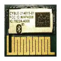


CYBLE-214015-01
BLUETOOTH MODULE, V4.2/1MBPS/1.71 - 5.5V
- Manufacturer: INFINEON
- Product type: Bluetooth Modules & Adaptors
- SVHC: No SVHC (25-Jun-2025)
- Interfaces: I2C, SPI, UART
- Product Range: EZ-BLE Series
- Certifications: CE, FCC, IC, KC, MIC
- Bluetooth Class: -
- Bluetooth Version: Bluetooth LE 4.2
- Supply Voltage Range: 1.71 V to 5.5 V
- Receiver Sensitivity Rx: -87 dBm
- Operating Temperature Range: -40 °C to 85 °C
| Delivery and price | |
|---|---|
| Units per pack | 250 |
| Price | 7.84 € |
| Current stock | 10+ |
| Lead time | 30 days |
## **CYBLE-214015-01** A/™“| **AIROC™ Bluetooth® Low Energy module**
## **General description**
The AIRCO™ CYBLE-214015-01 is a fully certified and qualified module supporting Bluetooth® Low Energy wireless communication. The CYBLE-214015-01 is a turnkey solution and includes onboard crystal oscillators, trace antenna, passive components, and the PSoC™ 4 Bluetooth® LE. Refer to the PSoC™ 4 Bluetooth® LE **datasheet** for additional details on the capabilities of the PSoC™ 4 Bluetooth® LE device used on this module.
The AIROC™ Bluetooth® LE module is a scalable and reconfigurable platform architecture. It combines programmable and reconfigurable analog and digital blocks with flexible automatic routing. The CYBLE-214015-01 also includes digital programmable logic, high-performance analog-to-digital conversion (ADC), opamps with comparator mode, and standard communication and timing peripherals.
The CYBLE-214015-01 includes a royalty-free Bluetooth® LE stack compatible with Bluetooth® 4.2 and provides up to 25 GPIOs in a small 11 × 11 × 1.80 mm package. The CYBLE-214015-01 is drop-in compatible with the **CYBLE-014008-00** AIROC™ Bluetooth® LE modules.
The CYBLE-214015-01 is a complete solution and an ideal fit for applications seeking a highly integrated Bluetooth® LE wireless solution.
## **Features**
- Module description
- Module size: 11.0 mm × 11.0 mm × 1.80 mm (with shield)
- Drop-in compatible with **CYBLE-014008-00**
- 256-KB flash memory, 32-KB SRAM memory
- Up to 25 GPIOs configurable as open drain high/low, pull-up/pull-down, HI-Z analog, HI-Z digial, or strong output
- Bluetooth® 4.2 qualified single-mode module
- QDID: **79480**
- Declaration ID: **D032785**
- Certified to FCC, CE, MIC, KC, and ISED regulations
- Industrial temperature range: –40°C to +85°C
- 32-bit processor (0.9 DMIPS/MHz) with single-cycle 32-bit multiply, operating at up to 48 MHz
- Watchdog timer with dedicated internal low-speed oscillator (ILO)
- Two-pin SWD for programming
- Power consumption
- TX output power: –18 dbm to +3 dbm
- Received signal strength indicator (RSSI) with 1-dB resolution
- TX current consumption of 15.6 mA (radio only, 0 dbm)
- RX current consumption of 16.4 mA (radio only)
- Low power mode support
- Deep Sleep: 1.3 µA with watch crystal oscillator (WCO) on
- Hibernate: 150 nA with SRAM retention
- Stop: 60 nA with XRES wakeup
- Programmable analog
- Four opamps with reconfigurable high-drive external and high-bandwidth internal drive, comparator modes, and ADC input buffering capability; can operate in Deep Sleep mode
- 12-bit, 1-Msps SAR ADC with differential and single-ended modes; channel sequencer with signal averaging
- Two current DACs (IDACs) for general-purpose or capacitive sensing applications on any pin
- One low-power comparator that operate in Deep Sleep mode
Please read the Important Notice and Warnings at the end of this document page 1
Datasheet www.infineon.com
002-15923 Rev. *G 2023-06-01
**AIROC™ Bluetooth® Low Energy module**
## Features
- Programmable digital
- Four programmable logic blocks called universal digital blocks, (UDBs), each with eight macrocells and datapath
- Infineon-provided peripheral component library, user-defined state machines, and verilog input
- Capacitive sensing
- Capacitive sigma-delta (CSD) provides best-in-class SNR (> 5:1) and liquid tolerance
- Infineon-supplied software component makes capacitive-sensing design easy
- Automatic hardware-tuning algorithm (SmartSense)
- Segment LCD drive
- LCD drive supported on all GPIOs (common or segment)
- Operates in Deep Sleep mode with four bits per pin memory
- Serial communication
- Two independent run-time reconfigurable serial communication blocks (SCBs) with I[2] C, SPI, or UART functionality
- Timing and pulse-width modulation
- Four 16-bit timer, counter, pulse-width modulator (TCPWM) blocks
- Center-aligned, Edge, and Pseudo-random modes
- Comparator-based triggering of Kill signals for motor drive and other high-reliability digital logic applications
- Up to 25 programmable GPIOs
- Any GPIO pin can be CAPSENSE™, LCD, analog, or digital
Datasheet
002-15923 Rev. *G
2
2023-06-01
**AIROC™ Bluetooth® Low Energy module**
More information
## **More information**
Infineon provides a wealth of data at **www.infineon.com** to help you to select the right module for your design, and to help you to quickly and effectively integrate the module into your design.
- Overview: **AIROC™ Bluetooth® & Multiprotocol**
- **PSoC™ 4 Bluetooth® LE Silicon Datasheet**
- Application notes: Infineon offers a number of Bluetooth[] LE application notes covering a broad range of topics, from basic to advanced level. Recommended application notes for getting started with AIROC Bluetooth[] LE modules are:
- **AN96841** - Getting started with AIROC™ Bluetooth® LE module
- **AN91267** - Getting started with PSoC™ 4 Bluetooth® LE
- **AN97060** - PSoC™ 4 Bluetooth® LE - Over-The-Air (OTA) Device Firmware Upgrade (DFU) guide
- **AN91162** - Creating a AIROC™ Bluetooth® LE custom profile
- **AN91184** - PSoC™ 4 Bluetooth® LE - Designing Bluetooth® LE applications
- **AN92584** - Designing for low power and estimating battery life for Bluetooth® LE applications
- **AN85951** - PSoC™ 4 CAPSENSE™ design guide
- **AN95089** - PSoC™ 4 Bluetooth® LE crystal oscillator selection and tuning techniques
- **AN91445** - Antenna design and RF layout guidelines
- Technical reference manual (TRM):
- PSoC™ 4 Bluetooth® LE **Technical Reference Manual**
- PSoC™ 4 Bluetooth® LE Registers **Technical Reference Manual**
- Knowledge base articles
- **KBA210574** - RF regulatory certifications for CYBLE-014008-00, CYBLE-214009-00, and CYBLE-214015-01 EZ-BLE™ PSoC™ modules
- **KBA216236** - Pin mapping differences between the EZ-BLE™ creator evaluation board (CYBLE-214015- EVAL) and the Bluetooth® LE pioneer kit (CY8CKIT-042-Bluetooth LE)
- **KBA97095** - AIROC™ Bluetooth® LE module placement
- **KBA213976** - FAQ for Bluetooth® LE and regulatory certifications with EZ-BLE™ modules
- **KBA210802** - Queries on Bluetooth® LE qualification and declaration processes
- **KBA218122** - 3D model files for AIROC™ Bluetooth® LE modules
- Development kits:
- **CYBLE-214015-EVAL** , CYBLE-214015-01 evaluation board
- **CY8CKIT-042-Bluetooth® LE** , Bluetooth® LE pioneer kit
- **CY8CKIT-002** , PSoC™ MiniProg3 program and debug kit
- Test and debug tools:
- **CYSmart** , AIROC™ Bluetooth® connect app - Bluetooth® LE test and debug tool
- **CYSmart Mobile** , AIROC™ Bluetooth® connect app - Mobile app
Two easy-to-use design environments to get you started quickly
## **PSoC™ Creator integrated design environment (IDE)**
**PSoC™ Creator** is an integrated design environment (IDE) that enables concurrent hardware and firmware editing, compiling and debugging of PSoC™ 3, PSoC™ 4, PSoC™ 5LP, PSoC™ 4 Bluetooth® LE, and EZ-BLE™ module systems with no code size limitations. PSoC™ peripherals are designed using schematic capture and simple graphical user interface (GUI) with over 120 pre-verified, production-ready PSoC™ components.
PSoC™ components are analog and digital “virtual chips,” represented by an icon that users can drag-and-drop into a design and configure to suit a broad array of application requirements.
Datasheet
002-15923 Rev. *G 2023-06-01
3
**AIROC™ Bluetooth® Low Energy module**
More information
## **Bluetooth** ® **LE component**
The **Bluetooth® Low Energy Component** inside PSoC™ creator provides a comprehensive GUI-based configuration window that lets you quickly design Bluetooth® LE applications. The component incorporates a Bluetooth® core specification v4.2 compliant Bluetooth® LE protocol stack and provides API functions to enable user applications to interface with the underlying Bluetooth® Low Energy Sub-System (BLESS) hardware via the stack.
## **AIROC™ Wi-Fi & Bluetooth® EZ-Serial module firmware platform**
The **AIROC™ Wi-Fi & Bluetooth® EZ-Serial module firmware platform** provides a simple way to access the most common hardware and communication features needed in Bluetooth® LE applications. This implements an intuitive API protocol over the UART interface and exposes various status and control signals through the module’s GPIOs, making it easy to add Bluetooth® LE functionality quickly to existing designs.
Use a simple serial terminal and evaluation kit to begin development without requiring an IDE. Refer to the AIROC™ Wi-Fi & Bluetooth® EZ-Serial module firmware platform web page for user manuals and instructions for getting started as well as detailed reference materials.
AIROC™ Bluetooth® LE modules are pre-flashed with the AIROC™ Wi-Fi & Bluetooth® EZ-Serial module firmware platform. If you do not have AIROC™ Wi-Fi & Bluetooth® EZ-Serial module firmware platform pre-loaded on your module, you can download each AIROC™ Bluetooth® LE module’s firmware images on the **AIROC™ Wi-Fi & Bluetooth® EZ-Serial module firmware platform** .
## **Technical support**
- **Forum** : See if your question is already answered by fellow developers on the PSoC 4 Bluetooth LE.
- Visit our **support** page and create a **technical support case** or contact a **local sales representatives** . If you are in the United States, you can talk to our technical support team by calling our toll-free number: +1-800-541-4736. Select option 2 at the prompt.
Datasheet
002-15923 Rev. *G
4
2023-06-01
**AIROC™ Bluetooth® Low Energy module**
Table of contents
## **Table of contents**
**General description ...........................................................................................................................1 Features ...........................................................................................................................................1 More information ..............................................................................................................................3 Table of contents...............................................................................................................................5 1 Overview .......................................................................................................................................8** 1.1 Module description.................................................................................................................................................8 1.1.1 Module dimensions and drawing........................................................................................................................8 **2 Pad connection interface...............................................................................................................10 3 Recommended host PCB layout......................................................................................................11 4 Digital and analog capabilities and connections ..............................................................................14 5 Power supply connections and recommended external components.................................................16** 5.1 Connection options ..............................................................................................................................................16 5.2 External component recommendation ...............................................................................................................16 5.3 Critical components list........................................................................................................................................19 5.4 Antenna design .....................................................................................................................................................19 **6 Electrical specification ..................................................................................................................20** 6.1 GPIO.......................................................................................................................................................................23 6.2 XRES.......................................................................................................................................................................24 6.3 Analog peripherals................................................................................................................................................24 6.3.1 Opamp................................................................................................................................................................24 6.3.2 Temperature sensor ..........................................................................................................................................27 6.3.3 SAR ADC..............................................................................................................................................................27 6.3.4 CSD .....................................................................................................................................................................28 6.4 Digital peripherals.................................................................................................................................................29 6.4.1 Timer ..................................................................................................................................................................29 6.4.2 Counter ..............................................................................................................................................................29 6.4.3 Pulse width modulation (PWM) ........................................................................................................................29 6.4.4 LCD direct drive..................................................................................................................................................30 6.5 Serial communication ..........................................................................................................................................31 6.6 Memory..................................................................................................................................................................32 6.7 System Resources.................................................................................................................................................34 6.7.1 Power-on-reset (POR) .......................................................................................................................................34 6.7.2 ............................................................................................................................................................................34 6.7.3 Voltage monitors (LVD) .....................................................................................................................................34 6.7.4 SWD interface ....................................................................................................................................................36 6.7.5 Internal main oscillator .....................................................................................................................................36 6.7.6 Internal low-speed oscillator ...........................................................................................................................36 **7 Environmental specifications ........................................................................................................41** 7.1 Environmental compliance..................................................................................................................................41 7.2 RF certification......................................................................................................................................................41 7.3 Environmental conditions....................................................................................................................................41 7.4 ESD and EMI protection........................................................................................................................................41 **8 Regulatory information.................................................................................................................42** 8.1 FCC.........................................................................................................................................................................42 8.2 ISED........................................................................................................................................................................43 8.3 European R&TTE Declaration of Conformity.......................................................................................................43 8.4 MIC Japan..............................................................................................................................................................44 8.5 KC Korea................................................................................................................................................................44 **9 Packaging ....................................................................................................................................45 10 Ordering information ..................................................................................................................47** 10.1 Part numbering convention ...............................................................................................................................47
Datasheet
002-15923 Rev. *G
5
2023-06-01
**AIROC™ Bluetooth® Low Energy module**
Table of contents
**11 Acronyms ...................................................................................................................................48 12 Document Conventions ...............................................................................................................52** 12.1 Units of Measure .................................................................................................................................................52 **13 Revision history..........................................................................................................................53 14 Sales, solutions, and legal information .........................................................................................54** 14.1 Worldwide sales and design support.................................................................................................................54 14.2 Products ..............................................................................................................................................................54 14.3 PSoC™ solutions..................................................................................................................................................55 14.4 Infineon developer community..........................................................................................................................55 14.5 Technical support...............................................................................................................................................55
Datasheet
002-15923 Rev. *G 2023-06-01
6
**AIROC™ Bluetooth® Low Energy module**
Overview
## **1 Overview**
## **1.1 Module description**
The CYBLE-214015-01 is a complete module designed to be soldered to the main host board.
## **1.1.1 Module dimensions and drawing**
Infineon reserves the right to select components (including the appropriate Bluetooth® LE device) from various vendors to achieve the Bluetooth® LE module functionality. Such selections will guarantee that all height restrictions of the component area are maintained. Designs should be completed with the physical dimensions shown in the mechanical drawings in **Figure 1** . All dimensions are in millimeters (mm).
|**Table 1**<br>**Module design dimensions**|**Table 1**<br>**Module design dimensions**||
|---|---|---|
|**Dimension item**||**Specification**|
|Module dimensions|Length (X)<br>~~—~~|11.00 ± 0.15 mm|
||Width (Y)<br>~~——~~|11.00 ± 0.15 mm|
|Antenna location dimensions|Length (X)<br>~~——~~<br>~~—~~|11.00 ± 0.15 mm|
||Width (Y)<br>~~—~~|4.62 ± 0.15 mm|
|PCB thickness|Height (H)<br>~~—~~|0.80 ± 0.10 mm|
|Shield height|Height (H)<br>~~——~~|1.00 ± 0.10 mm|
|Maximum component height|Height (H)<br>~~—~~|1.00 mm typical (shield)|
|Total module thickness (bottom of module to highest<br>component)|Height (H)<br>~~|~~|1.80 mm typical|
See **Figure 1** for the mechanical reference drawing for CYBLE-214015-01.
Datasheet
002-15923 Rev. *G
7
2023-06-01
**AIROC™ Bluetooth® Low Energy module**
Overview
**Figure 1 Module mechanical drawing**
## **Note**
1. No metal should be located beneath or above the antenna area. Only bare PCB material should be located beneath the antenna area. For more information on recommended host PCB layout, see **Figure 3** , **Figure 4** , **Figure 5** , **Figure 6** , and **Table 3** .
Datasheet
002-15923 Rev. *G 2023-06-01
8
**AIROC™ Bluetooth® Low Energy module**
Pad connection interface
## **2 Pad connection interface**
As shown in the bottom view of **Figure 1** , the CYBLE-214015-01 connects to the host board via solder pads on the back of the module. **Table 2** and **Figure** detail the solder pad length, width, and pitch dimensions of the CYBLE-214015-01 module.
## **Table 2 Solder pad connection description**
|**Name**|**Connections **|**Connection type**|**Pad length dimension**|**Pad width dimension**|**Pad pitch**|
|---|---|---|---|---|---|
|SP|32|Solder pads|Pad9/Pad24: 0.74 mm<br>All others: 0.79 mm|0.41 mm|0.66 mm|
**Figure 2 Solder pad dimensions (bottom view)**
To maximize RF performance, the host layout should follow these recommendations:
1. The ideal placement of the AIROC™ Bluetooth® LE module is in a corner of the host board with the antenna located on the edge of the host board. This placement minimizes the additional recommended keep-out area stated in item 2. Refer to **AN96841** for module placement best practices.
2. To maximize RF performance, the area immediately around the AIROC™ Bluetooth® LE module trace antenna should contain an additional keep-out area, where no grounding or signal traces are contained. The keep-out area applies to all layers of the host board. The recommended dimensions of the host PCB keep-out area are shown in **Figure 3** (dimensions are in mm).
**Figure 3 Recommended host PCB keep-out area around the CYBLE-214015-01 trace antenna**
Datasheet
002-15923 Rev. *G
9
2023-06-01
**AIROC™ Bluetooth® Low Energy module**
Recommended host PCB layout
## **3 Recommended host PCB layout**
**Figure 4** through **Figure 6** and **Table 3** provide details that can be used for the recommended host PCB layout pattern for the CYBLE-214015-01. Dimensions are in millimeters unless otherwise noted. Pad length of 0.99 mm (0.494 mm from center of the pad on either side) shown in **Figure 6** is the minimum recommended host pad length. The host PCB layout pattern can be completed using either **Figure 4** , **Figure 5** , or **Figure 6** . It is not necessary to use all figures to complete the host PCB layout pattern.
**Figure 4 Host layout pattern for CYBLE-214015-01**
**Figure 5 Module pad location from origin**
Datasheet
002-15923 Rev. *G
10
2023-06-01
**AIROC™ Bluetooth® Low Energy module**
Recommended host PCB layout
**Table 3** provides the center location for each solder pad on the CYBLE-214015-01. All dimensions are referenced to the center of the solder pad. Refer to **Figure 6** for the location of each module solder pad.
## **Module solder pad location**
|**Solder pad (center of pad)**|**Location (X,Y) from orign (mm)**<br>~~a~~|**Dimension from orign (mils)**|
|---|---|---|
|1|(0.30, 4.83)<br>~~a~~<br>~~—_~~|(11.81, 190.16)|
|2|(0.30, 5.49)<br>~~—_~~<br>~~TT~~|(11.81, 216.14)|
|3|(0.30, 6.15)<br>~~—~~|(11.81, 242.13)|
|4|(0.30, 6.81)<br>~~—_~~|(11.81, 268.11)|
|5|(0.30, 7.47)<br>~~—_~~|(11.81, 294.09)|
|6|(0.30, 8.13)<br>~~—_~~<br>~~TT~~|(11.81, 320.08)|
|7|(0.30, 8.79)<br>~~—~~|(11.81, 346.06)|
|8|(0.30, 9.45)<br>~~—_~~|(11.81, 372.05)|
|9|(0.27, 10.11)<br>~~—_~~|(10.63, 398.03)|
|10|(1.21, 10.70)<br>~~—_~~<br>~~TT~~|(47.64, 421.26)|
|11|(1.87, 10.70)<br>~~—~~|(73.62, 421.26)|
|12|(2.53, 10.70)<br>~~—_~~|(99.61, 421.26)|
|13|(3.19, 10.70)<br>~~—_~~|(125.59, 421.26)|
|14|(3.85, 10.70)<br>~~TT~~|(151.57, 421.26)|
|15|(4.51, 10.70)<br>~~—~~|(177.56, 421.26)|
|16|(5.17, 10.70)<br>~~—_~~|(203.54, 421.26)|
|17|(5.84, 10.70)<br>~~—_~~|(229.92, 421.26)|
|18|(6.50, 10.70)<br>~~TT~~|(255.91, 421.26)|
|19|(7.16, 10.70)<br>~~—~~|(281.89, 421.26)|
|20|(7.82, 10.70)<br>~~—_~~|(307.87, 421.26)|
|21|(8.48, 10.70)<br>~~—_~~|(333.86, 421.26)|
|22|(9.14, 10.70)<br>~~TT~~|(359.84, 421.26)|
|23|(9.80, 10.70)<br>~~—~~|(385.83, 421.26)|
|24|(10.73, 10.11)<br>~~—~~|(422.44, 398.03)|
|25|(10.70, 9.45)<br>~~—_~~|(421.26, 372.05)|
|26|(10.70, 8.79)<br>~~—_~~|(421.26, 346.06)|
|27|(10.70, 8.13)<br>~~TT~~|(421.26, 320.08)|
|28|(10.70, 7.47)<br>~~—~~|(421.26, 294.09)|
|29|(10.70, 6.81)<br>~~—_~~|(421.26, 268.11)|
|30|(10.70, 6.15)<br>~~—_~~|(421.26, 242.13)|
|31|(10.70, 5.49)<br>~~TT~~|(421.26, 216.14)|
|32|(10.70, 4.83)<br>~~—~~|(421.26, 190.16)|
Datasheet
002-15923 Rev. *G 2023-06-01
11
**AIROC™ Bluetooth® Low Energy module**
Recommended host PCB layout
**Figure 6 Solder pad reference location**
Datasheet
002-15923 Rev. *G 2023-06-01
12
**AIROC™ Bluetooth® Low Energy module**
Digital and analog capabilities and connections
## **4 Digital and analog capabilities and connections**
**Table 4** and **Table 5** detail the solder pad connection definitions and available functions for each connection pad. **Table 4** lists the solder pads on CYBLE-214015-01, the AIROC™ Bluetooth® LE device port-pin, and denotes whether the digital function shown is available for each solder pad. **Table 5** denotes whether the analog function shown is available for each solder pad. Each connection is configurable for a single option shown with a ✓.
## **Table 4 Digital peripheral capabilities**
|**Pad num-**<br>**ber**<br>~~|~~|**Device**<br>**port pin**<br>~~|~~|**UART**|**SPI**|**I2C**|**TCPWM**[2,3]|**CAP-**<br>**SENSE™**|**WCO Out**|**ECO Out**|**LCD**|**SWD**|**GPIO**|
|---|---|---|---|---|---|---|---|---|---|---|---|
|1<br>~~|~~|GND[4]<br>~~|ee~~|Ground connection<br>~~ee~~<br>~~re~~<br>~~rsrsI~~||||||||||
|2<br>~~|~~|P1.1<br>~~|ee~~<br>~~a~~|~~ee~~<br>~~ee~~|✓(SCB1_SS1)<br>~~re~~<br>~~es~~|~~rs~~<br>~~es~~|✓(TCPWM)<br>~~rs~~<br>~~rs~~|✓<br>~~I~~<br>~~I~~|||✓||✓|
|3<br>|P1.0<br>~~ee~~<br>~~a~~<br>~~ee~~|~~ee~~<br>~~ee~~|~~re~~<br>~~es~~<br>~~rs~~|~~rs ~~<br>~~es~~<br>~~rs~~|✓(TCPWM)<br> ~~rs ~~<br>~~rs~~<br>~~rs~~|✓<br> ~~I~~<br>~~I~~|||✓||✓|
|4|P1.5<br>~~a~~<br>~~ee~~<br>~~ee~~|✓(SCB0_TX)<br>~~ee~~<br>~~ne~~|✓(SCB0_MISO)<br>~~es~~<br>~~rs~~<br>~~ne rs~~|✓(SCB0_SCL)<br>~~es~~<br>~~rs~~<br>~~rs~~|✓(TCPWM)<br>~~rs ~~<br>~~rs~~<br>~~Gt~~|✓<br> ~~I~~|~~I~~|~~I~~|✓||✓|
|5|P0.1<br>~~ee~~<br>~~ee~~<br>~~a~~|✓(SCB1_TX)<br>~~ne~~<br>~~ee~~|✓(SCB1_MISO)<br>~~rs~~<br>~~ne rs~~<br>~~ee~~|✓(SCB1_SCL)<br>~~rs~~<br>~~rs~~<br>~~es ee~~|✓(TCPWM)<br>~~rs~~<br>~~Gt~~<br>~~ee~~|✓<br>~~ee~~|~~I~~<br>~~ee~~|~~I~~<br>~~ee~~|✓<br>~~ee~~|~~ee~~|✓|
|6|P0.7<br>~~ee~~<br>~~a~~|✓(SCB0_CTS)<br>~~ne~~<br>~~ee~~|✓(SCB0_SCLK)<br>~~ne rs~~<br>~~ee~~|~~rs~~<br>~~es ee~~|✓(TCPWM)<br>~~Gt~~<br>~~ee~~|✓<br>~~ee~~|~~I~~<br>~~ee~~|~~I~~<br>~~ee~~|✓<br>~~ee~~|✓<br>(SWDCLK)<br>~~ee~~|✓|
|7|VDD<br>~~a~~<br>~~ee~~|Digital power supply input (1.71 V to 5.5 V)<br>~~ee~~<br>~~ee es ee ee ee~~<br>~~esrns ts(I~~||||||||||
|8|P1.4<br>~~ee~~<br>~~ee~~|✓(SCB0_RX)<br>~~es~~<br>~~ee~~|✓(SCB0_MOSI)<br>~~es~~<br>~~rs~~|✓(SCB0_SDA)<br>~~rns ts~~<br>~~rs~~|✓(TCPWM)<br>~~ts~~<br>~~rs~~|✓<br>~~(I~~<br>~~I~~|||✓||✓|
|9|P0.4<br>~~ee~~<br>~~ee~~<br>~~ee~~|✓(SCB0_RX)<br>~~es~~<br>~~ee~~<br>~~ee~~|✓(SCB0_MOSI)<br>~~es ~~<br>~~rs~~<br>~~ee es~~|✓(SCB0_SDA)<br> ~~rns ts~~<br>~~rs~~<br>~~es~~|✓(TCPWM)<br>~~ts~~<br>~~rs~~<br>~~rs~~|✓<br>~~(I~~<br>~~I~~<br>~~rd~~||✓|✓||✓|
|10|P0.5<br>~~ee~~<br>~~ee~~<br>~~a~~|✓(SCB0_TX)<br>~~ee~~<br>~~ee~~<br>~~ee~~|✓(SCB0_MISO)<br>~~rs~~<br>~~ee es~~<br>~~ee es~~|✓(SCB0_SCL)<br>~~rs~~<br>~~es~~<br>~~es~~|✓(TCPWM)<br>~~rs ~~<br>~~rs~~<br>~~ee~~|✓<br> ~~I~~<br>~~rd~~<br>~~ee~~|~~ee~~|~~ee~~|✓||✓|
|11|P0.6<br>~~ee~~<br>~~a~~<br>~~ee~~|✓(SCB0_RTS)<br>~~ee~~<br>~~ee~~<br>~~ee~~|✓(SCB0_SS0)<br>~~ee es~~<br>~~ee es~~<br>~~ne~~|~~es~~<br>~~es~~<br>~~rs~~|✓(TCPWM)<br>~~rs~~<br>~~ee~~<br>~~rs~~|✓<br>~~rd~~<br>~~ee~~<br>~~rn~~|~~ee~~|~~ee~~|✓|✓<br>(SWDIO)|✓|
|12|P1.2<br>~~a~~<br>~~ee~~|~~ee~~<br>~~ee~~|✓(SCB1_SS2)<br>~~ee es~~<br>~~ne~~|~~es ~~<br>~~rs~~|✓(TCPWM)<br> ~~ee ~~<br>~~rs~~|✓<br> ~~ee ~~<br>~~rn~~|~~ee~~|~~ee~~|✓||✓|
|13|VDDR<br>~~ee~~<br>~~ee~~|Radio power supply (1.9 V to 5.5 V)<br>~~ee~~<br>~~ne~~<br>~~rs~~<br>~~rs~~<br>~~rn~~<br>~~eeee~~<br>~~rs~~<br>~~rsrn~~||||||||||
|14|P2.6<br>~~ee~~<br>~~ee~~|~~ee~~<br>~~ne~~|~~ee~~<br>~~ne rs~~|~~rs~~<br>~~rs~~|✓(TCPWM)<br>~~rs~~<br>~~Gt~~|✓<br>~~rn~~|~~I~~|~~I~~|✓||✓|
|15|P1.3<br>~~ee~~<br>~~ee~~<br>~~ee~~|~~ee~~<br>~~ne~~<br>~~ee~~|✓(SCB1_SS3)<br>~~ee~~<br>~~ne rs~~<br>~~re~~|~~rs~~<br>~~rs~~<br>~~re~~|✓(TCPWM)<br>~~rs ~~<br>~~Gt~~<br>~~rs~~|✓<br> ~~rn~~<br>~~I~~|~~I~~|~~I~~|✓||✓|
|16|P3.0<br>~~ee~~<br>~~ee~~<br>~~a~~|✓(SCB0_RX)<br>~~ne~~<br>~~ee~~<br>~~ee~~|~~ne rs~~<br>~~re~~<br>~~es~~|✓(SCB0_SDA)<br>~~rs~~<br>~~re~~<br>~~es~~|✓(TCPWM)<br>~~Gt~~<br>~~rs~~<br>~~rs~~|✓<br>~~I~~<br>~~I~~|~~I~~|~~I~~|✓||✓|
|17|P2.1<br>~~ee~~<br>~~a~~<br>~~ee~~|~~ee~~<br>~~ee~~|✓(SCB0_SS2)<br>~~re~~<br>~~es~~<br>~~rs~~|~~re~~<br>~~es~~<br>~~rs~~|✓(TCPWM)<br>~~rs ~~<br>~~rs~~<br>~~rs~~|✓<br> ~~I~~<br>~~I~~|||✓||✓|
|18|P2.2<br>~~a~~<br>~~ee~~<br>~~ee~~|~~ee~~|✓(SCB0_SS3)<br>~~es~~<br>~~rs~~<br>~~re~~|~~es~~<br>~~rs~~<br>~~rs~~|✓(TCPWM)<br>~~rs ~~<br>~~rs~~<br>~~(ns~~|✓<br> ~~I~~<br>~~I~~|~~I~~|~~I~~|✓||✓|
|19|P2.3<br>~~ee~~<br>~~ee~~||~~rs~~<br>~~re~~|~~rs~~<br>~~rs~~|✓(TCPWM)<br>~~rs~~<br>~~(ns~~|✓<br>~~I~~|✓<br>~~I~~|~~I~~|✓||✓|
|20|VDDA<br>~~ee~~<br>~~ee ee~~|Analog power supply input (1.71 V to 5.5 V)<br>~~re~~<br>~~rs(ns I~~<br>~~I~~<br>~~ee~~<br>~~es~~<br>~~rsI~~||||||||||
|21|P3.4<br>~~ee ee~~<br>~~ee~~|✓(SCB1_RX)<br>~~ee~~|~~es~~<br>~~rs~~|✓(SCB1_SDA)<br>~~es~~<br>~~rs~~|✓(TCPWM)<br>~~rs~~<br>~~rs~~|✓<br>~~I~~|||✓||✓|
|22|P3.1<br>~~ee ee~~<br>~~ee~~<br>~~ee~~|✓(SCB0_TX)<br>~~ee~~<br>~~ne~~|~~es~~<br>~~rs~~<br>~~ne rs~~|✓(SCB0_SCL)<br>~~es~~<br>~~rs~~<br>~~rs~~|✓(TCPWM)<br>~~rs ~~<br>~~rs~~<br>~~Gt~~|✓<br> ~~I~~|~~I~~|~~I~~|✓||✓|
|23|P3.7<br>~~ee~~<br>~~ee~~<br>~~ee~~|✓(SCB1_CTS)<br>~~ne~~<br>~~ee~~|~~rs~~<br>~~ne rs~~<br>~~re~~|~~rs~~<br>~~rs~~<br>~~rs~~|✓(TCPWM)<br>~~rs~~<br>~~Gt~~<br>~~rs~~|✓<br>~~I~~|✓<br>~~I~~|~~I~~|✓||✓|
|24|P3.5<br>~~ee~~<br>~~ee~~<br>~~ee~~|✓(SCB1_TX)<br>~~ne~~<br>~~ee~~<br>~~ee ne~~|~~ne rs~~<br>~~re~~<br>~~ne~~|✓(SCB1_SCL)<br>~~rs~~<br>~~rs~~<br>~~rs~~|✓(TCPWM)<br>~~Gt~~<br>~~rs~~<br>~~rs~~|✓<br>~~I~~|~~I~~<br>~~I~~|~~I~~<br>~~I~~|✓||✓|
|25|P3.3<br>~~ee~~<br>~~ee~~|✓(SCB0_CTS)<br>~~ee~~<br>~~ee ne~~|~~re ~~<br>~~ne~~|~~rs~~<br>~~rs~~|✓(TCPWM)<br>~~rs ~~<br>~~rs~~|✓<br> ~~I~~|~~I~~|~~I~~|✓||✓|
|26|VREF<br>~~ee~~<br>~~ee~~|Reference voltage input<br>~~ee ne~~<br>~~rs~~<br>~~rs~~<br>~~I~~<br>~~ee~~<br>~~re~~<br>~~rsrsI~~||||||||||
|27|P3.2<br>~~ee~~|✓(SCB0_RTS)<br>~~ee~~|~~re~~|~~rs~~|✓(TCPWM)<br>~~rs~~|✓<br>~~I~~|||✓||✓|
|28<br>~~|~~|P3.6<br>~~ee~~<br>~~|~~|✓(SCB1_RTS)<br>~~ee~~|~~re~~|~~rs ~~|✓(TCPWM)<br> ~~rs ~~|✓<br> ~~I~~|||✓||✓|
|29<br>~~|~~|XRES<br>~~|ee~~|External reset hardware connection input<br>~~rr~~<br>~~rs nrI~~||||||||||
|30<br>~~|~~|P2.4<br>~~|ee~~|~~rr~~|~~rr~~|~~rs nr~~|✓(TCPWM)<br>~~nr~~|✓<br>~~I~~|||✓||✓|
|31<br><br>~~|~~|P2.5<br>~~ee~~<br>~~|~~|~~rr~~|~~rr~~|~~rs nr~~|✓(TCPWM)<br>~~nr ~~|✓<br> ~~I~~|||✓||✓|
|32<br>~~|~~|GND[4]<br>~~|~~|Ground connection||||||||||
Datasheet
002-15923 Rev. *G
13
2023-06-01
**AIROC™ Bluetooth® Low Energy module**
Digital and analog capabilities and connections
|**Pad number**|**Device port pin**<br>~~eG~~|**SARMUX**<br>~~eG~~|**OPAMP**<br>~~eG~~|**LPCOMP**|
|---|---|---|---|---|
|1|GND[4]<br>~~PY~~<br>~~ee~~|Ground connection<br>~~Gs~~|||
|2|P1.1<br>~~PY~~<br>~~ee~~<br>~~ee~~|~~Gs~~<br>~~Gs~~|✓(CTBm1_OA0_INN)||
|3|P1.0<br>~~ee~~<br>~~ee~~|~~Gs~~<br>~~Gs~~|✓(CTBm1_OA0_INP)||
|4|P1.5<br>~~ee~~<br>~~eG~~|~~Gs~~<br>~~eG~~|✓(CTBm1_OA1_INP)<br>~~eG~~||
|5|P0.1<br>~~ee~~<br>~~ee~~|~~ee~~<br>~~Gs~~|~~ee~~||
|6|P0.7<br>~~ee~~<br>~~ee~~|~~ee~~<br>~~Gs~~|~~ee~~||
|7|VDD<br>~~ee~~<br>~~Pe~~|Digital power supply input (1.71 V to 5.5 V)<br>~~Gs~~|||
|8|P1.4<br>~~eG~~|~~eG~~|✓(CTBm1_OA1_INN)<br>~~eG~~||
|9|P0.4<br>~~ee~~<br>~~ee~~|~~ee~~<br>~~Gs~~|~~ee~~|✓(COMP1_INP)|
|10|P0.5<br>~~ee~~<br>~~ee~~<br>~~ee~~|~~ee~~<br>~~Gs~~<br>~~Gs~~|~~ee~~|✓(COMP1_INN)|
|11|P0.6<br>~~ee~~<br>~~ee~~|~~Gs~~<br>~~Gs~~|||
|12|P1.2<br>~~ee~~<br>~~Gn~~|~~Gs~~<br>~~Gn~~|✓(CTBm1_OA0_OUT)<br>~~Gn~~||
|13|VDDR<br>~~PY~~<br>~~ee~~|Radio power supply (1.9 V to 5.5 V)<br>~~Gs~~|||
|14|P2.6<br>~~PY~~<br>~~ee~~<br>~~ee~~|~~Gs~~<br>~~Gs~~|✓(CTBm0_OA0_INP)||
|15|P1.3<br>~~ee~~<br>~~ee~~|~~Gs~~<br>~~Gs~~|✓(CTBm1_OA1_OUT)||
|16|P3.0<br>~~ee~~<br>~~eG~~|✓<br>~~Gs~~<br>~~eG~~|~~eG~~||
|17|P2.1<br>~~ee~~<br>~~ee~~|~~ee~~<br>~~Gs~~|✓(CTBm0_OA0_INN)<br>~~ee~~||
|18|P2.2<br>~~ee~~<br>~~ee~~|~~Gs~~<br>~~Gs~~|✓(CTBm0_OA0_OUT)||
|19<br>~~PF~~|P2.3<br>~~ee~~<br>~~ee~~<br>~~PF~~|~~Gs~~<br>~~Gs~~<br>|✓(CTBm0_OA1_OUT)||
|20<br>~~PF~~|VDDA<br>~~ee~~<br>~~PFee~~|Analog Power Supply Input (1.71 V to 5.5 V)<br>~~Gs~~<br>~~Gs~~|||
|21<br>~~PF~~|P3.4<br>~~PFee~~<br>~~ee~~|✓<br>~~Gs~~<br>~~Gs~~|||
|22<br>|P3.1<br>~~ee~~<br>~~ee~~|✓<br>~~Gs~~<br>~~Gs~~<br>~~ee~~|~~ee~~||
|23|P3.7<br>~~ee~~<br>~~ee~~|✓<br>~~Gs~~<br>~~ee~~<br>~~ee~~<br>~~ee~~|~~ee~~<br>~~ee~~||
|24|P3.5<br>~~ee~~<br>~~PY~~|✓<br>~~ee~~<br>~~ee~~<br>~~ee~~<br>~~ee~~|~~ee~~<br>~~ee~~||
|25|P3.3<br>~~ee~~<br>~~PY~~|✓<br>~~ee~~<br>~~ee~~<br>~~ee~~|~~ee~~||
|26|VREF<br>~~PY~~|Reference voltage input (optional)<br>~~ee~~<br>~~ee~~<br>~~ee~~|||
|27|P3.2<br>~~ee~~<br>~~PY~~|✓<br>~~ee~~<br>~~ee~~<br>~~ee~~|~~ee~~<br>~~ee~~||
|28|P3.6<br>~~ee~~<br>~~PY~~|✓<br>~~ee~~<br>~~ee~~<br>~~ee~~|~~ee~~<br>~~ee~~||
|29|XRES<br>~~PY~~<br>~~ee~~|External reset hardware connection input<br>~~ee~~<br>~~Gs~~|||
|30|P2.4<br>~~ee~~|~~Gs~~|✓(CTBm0_OA1_INN)||
|31|P2.5<br>~~ee~~<br>~~Gn~~|~~Gs~~<br>~~Gn~~|✓(CTBm0_OA1_INP)<br>~~Gn~~||
|32|GND<br>~~Ps~~|Ground connection|||
## **Notes**
2. TCPWM stands for timer, counter, and PWM. If supported, the pad can be configured to any of these peripheral functions.
3. TCPWM connections on ports 0, 1, 2, and 3 can be routed through the Digital Signal Interconnect (DSI) to any of the TCPWM blocks and can be either positive or negative polarity.
4. The main board needs to connect both GND connections (Pad 1 and Pad 32) on the module to the common ground of the system.
Datasheet
002-15923 Rev. *G 2023-06-01
14
**AIROC™ Bluetooth® Low Energy module**
Power supply connections and recommended external components
## **5 Power supply connections and recommended external components**
## **Power connections**
The CYBLE-214015-01 contains three power supply connections, VDD, VDDA, and VDDR. The VDD and VDDA connections supply power for the digital and analog device operation respectively. VDDR supplies power for the device radio.
VDD and VDDA accept a supply range of 1.71 V to 5.5 V. VDDR accepts a supply range of 1.9 V to 5.5 V. These specifications can be found in **Table 10** . The maximum power supply ripple for both power connections on the module is 100 mV, as shown in **Table 8** .
The power supply ramp rate of VDD and VDDA must be equal to or greater than that of VDDR when the radio is used.
## **5.1 Connection options**
Two connection options are available for any application:
1. Single supply: Connect VDD, VDDA, and VDDR to the same supply.
2. Independent supply: Power VDD, VDDA, and VDDR separately.
## **5.2 External component recommendation**
In either connection scenario, it is recommended to place an external ferrite bead between the supply and the module connection. The ferrite bead should be positioned as close as possible to the module pin connection.
**Figure 7** details the recommended host schematic options for a single supply scenario. The use of one or three ferrite beads will depend on the specific application and configuration of the CYBLE-214015-01.
**Figure 8** details the recommended host schematic for an independent supply scenario.
The recommended ferrite bead value is 330 , 100 MHz (Murata BLM21PG331SN1D).
**Figure 7 Recommended host schematic options for single supply option**
Datasheet
002-15923 Rev. *G
15
2023-06-01
**AIROC™ Bluetooth® Low Energy module**
Power supply connections and recommended external components
**Figure 8 Recommended host schematic for independent supply option**
Datasheet
002-15923 Rev. *G
16
2023-06-01
**AIROC™ Bluetooth® Low Energy module**
Power supply connections and recommended external components
The CYBLE-214015-01 schematic is shown in **Figure 9** .
**Figure 9 CYBLE-214015-01 schematic diagram**
Datasheet
002-15923 Rev. *G 2023-06-01
17
**AIROC™ Bluetooth® Low Energy module**
Power supply connections and recommended external components
## **5.3 Critical components list**
**Table 6** details the critical components used in the CYBLE-214015-01 module.
|**Table 6**|**Table 6**|**Critical component list**|**Critical component list**|||
|---|---|---|---|---|---|
|||**Component**||**Reference designator**|**Description**|
|||Silicon||U1|76-pin WLCSP PSoC™with<br>BluetoothLE|
|||Crystal||Y1|24.000 MHz, 10PF|
|||Crystal||Y2|32.768 kHz, 12.5PF|
## **5.4 Antenna design**
**Table** details antenna used on the CYBLE-214015-01 module. The module performance improves many of these characteristics. For more information, see **Table 9** .
## **Table 7 Trace antenna specifications**
|**Trace antenna specifications**||
|---|---|
|**Item**|**Description**|
|Frequency range|2400 – 2500 MHz|
|Peakgain|0.5 dBi typical|
|Averagegain|–0.5 dBi typical|
|Return loss|10 dB minimum|
Datasheet
002-15923 Rev. *G 2023-06-01
18
**AIROC™ Bluetooth® Low Energy module**
Electrical specification
## **6 Electrical specification**
**Table 8** details the absolute maximum electrical characteristics for the AIROC™ Bluetooth® LE module.
|**Parameter**|**Description**<br>~~ee~~|**Min**<br>~~ee~~|**Typ**<br>~~ee~~|**Max**<br>~~ee~~|**Unit**<br>~~ee~~|**Details/conditions**|
|---|---|---|---|---|---|---|
|VDDD_ABS|VDD, VDDAor VDDRsupply relative<br>to VSS(VSSD= VSSA)<br>~~=~~|–0.5<br>~~=~~|–<br>~~=~~|6<br>~~=~~|V<br>~~=~~|Absolute maximum|
|VCCD_ABS|Direct digital core voltage input<br>relative to VSSD<br>~~ee~~|–0.5<br>~~ee~~|–<br>~~ee~~|1.95<br>~~ee~~|V<br>~~ee~~|Absolute maximum|
|VDDD_RIPPLE|Maximum power supply ripple for<br>VDD, VDDAand VDDRinput voltage<br>~~a~~|–<br>~~a~~|–<br>~~a~~|100<br>~~a~~|mV<br>~~a~~|3.0V supply<br>Ripple frequency of 100 kHz to<br>750 kHz|
|VGPIO_ABS|GPIO voltage<br>~~a~~<br>~~ee~~|–0.5<br>~~a~~<br>~~ee~~|–<br>~~a~~<br>~~ee~~|VDD<br>+0.5<br>~~a~~<br>~~ee~~|V<br>~~a~~<br>~~ee~~|Absolute maximum|
|IGPIO_ABS|Maximum current per GPIO<br>~~a~~|–25<br>~~a~~|–<br>~~a~~|25<br>~~a~~|mA<br>~~a~~|Absolute maximum|
|IGPIO_injection|GPIO injection current: Maximum<br>for VIH> VDDand minimum for VIL<br>< VSS<br>~~a~~|–0.5<br>~~a~~|–<br>~~a~~|0.5<br>~~a~~|mA<br>~~a~~|Absolute maximum current<br>injected per pin|
|LU|Pin current for latch up<br>~~po~~|–200<br>~~po~~|~~po~~|200<br>~~po~~|mA<br>~~po~~|–|
**Table 9** details the RF characteristics for the AIROC™ Bluetooth® LE module.
|**Parameter**|**Description**<br>~~ee~~|**Min**<br>~~ee~~|**Typ**<br>~~ee~~|**Max**<br>~~ee~~|**Unit**<br>~~ee~~|**Details/conditions**|
|---|---|---|---|---|---|---|
|RFO|RF output power on ANT<br>~~=~~|–18<br>~~=~~|0<br>~~=~~|3<br>~~=~~|dBm<br>~~=~~|Configurable via register<br>settings|
|RXS|RF receive sensitivity on ANT<br>~~ee~~|–<br>~~ee~~|–87<br>~~ee~~|–<br>~~ee~~|dBm<br>~~ee~~|Guaranteed by design<br>simulation|
|FR|Module frequency range<br>~~rr~~|2400<br>~~rr~~|–<br>~~rr~~|2480<br>~~rr~~|MHz<br>~~rr~~|–|
|GP|Peakgain<br>~~rr~~|–<br>~~rr~~|0.5<br>~~rr~~|–<br>~~rr~~|dBi<br>~~rr~~|–|
|GAvg|Averagegain<br>~~ee~~|–<br>~~ee~~|–0.5<br>~~ee~~|–<br>~~ee~~|dBi<br>~~ee~~|–|
|RL|Return loss<br>~~ee~~|–<br>~~ee~~|–10<br>~~ee~~|–<br>~~ee~~|dB<br>~~ee~~|–|
|RFO|RF output power on ANT<br>~~ee~~|–18<br>~~ee~~|0<br>~~ee~~|3<br>~~ee~~|dBm<br>~~ee~~|Configurable via register<br>settings|
**Table 10** through **Table 51** list the module level electrical characteristics for the CYBLE-214015-01. All specifications are valid for –40°C ≤ TA ≤ 85°C and TJ ≤ 100°C, except where noted. Specifications are valid for 1.71 V to 5.5 V, except where noted.
## **Table 10 CYBLE-214015-01 DC specifications**
|**Parameter**|**Description**|**Min**|**Typ**|**Max**|**Unit**|**Details/conditions**|
|---|---|---|---|---|---|---|
|VDD1|Power supply input voltage (VDD<br>=VDDA=VDDR)|1.71|–|5.5|V|With regulator enabled|
|VDD2|Power supply input voltage<br>unregulated (VDD=VDDA=VDDR)|1.71|1.8|1.89|V|Internally unregulated supply|
|VDDR1|Radio supply voltage (radio on)|1.9|–|5.5|V|–|
Datasheet
002-15923 Rev. *G
19
2023-06-01
**AIROC™ Bluetooth® Low Energy module**
Electrical specification
**Table 10 CYBLE-214015-01 DC specifications** _(continued)_
**==> picture [511 x 668] intentionally omitted <==**
**----- Start of picture text -----**<br>
|||||||||
|---|---|---|---|---|---|---|---|
|Parameter|Description|Min|Typ|Max|Unit|Details/conditions|
|VDDR2|Radio supply voltage (radio off)|1.71|–|5.5|V|–|
|Active mode, VDD = 1.71 V to 5.5 V|
|IDD3|Execute from flash; CPU at 3 MHz|–|1.7|–|mA|T = 25°C, VDD = 3.3V|
|IDD4|Execute from flash; CPU at 3 MHz|–|–|–|mA|T = –40°C to 85°C|
|IDD5|Execute from flash; CPU at 6 MHz|–|2.5|–|mA|T = 25°C, VDD = 3.3V|
|IDD6|Execute from flash; CPU at 6 MHz|–|–|–|mA|T = –40°C to 85°C|
|IDD7|Execute from flash; CPU at 12 MHz|–|4|–|mA|T = 25°C, VDD = 3.3V|
|IDD8|Execute from flash; CPU at 12 MHz|–|–|–|mA|T = –40°C to 85°C|
|IDD9|Execute from flash; CPU at 24 MHz|–|7.1|–|mA|T = 25°C, VDD = 3.3 V|
|IDD10|Execute from flash; CPU at 24 MHz|–|–|–|mA|T = –40°C to 85°C|
|IDD11|Execute from flash; CPU at 48 MHz|–|13.4|–|mA|T = 25°C, VDD = 3.3 V|
|IDD12|Execute from flash; CPU at 48 MHz|–|–|–|mA|T = –40°C to 85°C|
|Sleep mode, VDD = 1.71 V to 5.5 V|
|IDD13|IMO on|–|–|–|mA|T = 25°C, VDD = 3.3 V, SYSCLK =|
|3 MHz|
|a|Sleep mode, VDD and VDDR = 1.9 V to 5.5 V|
|IDD14|ECO on|–|–|–|mA|T = 25°C, VDD = 3.3 V, SYSCLK = 3|
|MHz|
|aee|Deep Sleep mode, VDD = 1.71 V to 3.6 V|
|IDD15|WDT with WCO on|–|1.3|–|µA|T = 25°C, VDD = 3.3 V|
|IDD16|WDT with WCO on|–|–|–|µA|T = –40°C to 85°C|
|IDD17|WDT with WCO on|–|–|–|µA|T = 25°C, VDD = 5 V|
|IDD18|WDT with WCO on|–|–|–|µA|T = –40°C to 85°C|
|Deep Sleep mgode, VDD = 1.71 V to 1.89 V (Regulator bypassed)|
|IDD19|WDT with WCO on|–|–|–|µA|T = 25°C|
|———————|IDD20|WDT with WCO on|–|–|–|µA|T = –40°C to 85°C|
|Hibernate mode, VDD = 1.71 V to 3.6 V|
|IDD27|GPIO and reset active|–|150|–|nA|T = 25°C, VDD = 3.3 V|
|————————|IDD28|GPIO and reset active|–|–|–|nA|T = –40°C to 85°C|
|Hibernate mode, VDD = 3.6 V to 5.5 V|
|IDD29|GPIO and reset active|–|–|–|nA|T = 25°C, VDD = 5 V|
|—————————————|IDD30|GPIO and reset active|–|–|–|nA|T = –40°C to 85°C|
|Stop mode, VDD = 1.71 V to 3.6 V|
|IDD33|Stop-mode current (VDD)|–|20|–|nA|T = 25°C, VDD = 3.3 V|
|IDD34|Stop-mode current (VDDR)|–|40|–-|nA|T = 25°C, VDDR = 3.3 V|
|IDD35|Stop-mode current (VDD)|–|–|–|nA|T = –40°C to 85°C|
|IDD36|Stop-mode current (VDDR)|–|–|–|nA|T = –40°C to 85°C, VDDR = 1.9 V to|
|3.6 V|
|Stop mode, VDD = 3.6 V to 5.5 V|
|IDD37|Stop-mode current (VDD)|–|–|–|nA|T = 25°C, VDD = 5 V|
|a|
**----- End of picture text -----**<br>
Datasheet
002-15923 Rev. *G
20
2023-06-01
**AIROC™ Bluetooth® Low Energy module**
Electrical specification
**Table 10 CYBLE-214015-01 DC specifications** _(continued)_
**==> picture [446 x 62] intentionally omitted <==**
**----- Start of picture text -----**<br>
||||||||
|---|---|---|---|---|---|---|
|Parameter|Description|Min|Typ|Max|Unit|Details/conditions|
|IDD38|Stop-mode current (VDDR)|–|–|–|nA|T = 25°C, VDDR = 5 V|
|IDD39|Stop-mode current (VDD)|–|–|–|nA|T = –40°C to 85°C|
|IDD40|Stop-mode current (VDDR)|–|–|–|nA|T = –40°C to 85°C|
**----- End of picture text -----**<br>
**Table 11 AC specifications Parameter** ~~SO~~ **Description Min Typ Max Unit Details/conditions** FCPU ~~TOT~~ CPU frequency DC – 48 MHz 1.71 V VDD 5.5 V TSLEEP Wakeup from Sleep mode – 0 – µs Guaranteed by characterization ~~— OTT EETTT~~ TDEEPSLEEP Wakeup from Deep Sleep mode – – 25 µs 24-MHz IMO. Guaranteed by characterization ~~FE~~ THIBERNATE ~~OT~~ Wakeup from Hibernate mode – – 800 µs Guaranteed by characterization TSTOP ~~TO~~ Wakeup from Stop mode – – 2 ms XRES wakeup ~~TE~~
Datasheet
002-15923 Rev. *G
21
2023-06-01
## **AIROC™ Bluetooth® Low Energy module**
Electrical specification
## **6.1 GPIO**
|**Table 12**|**GPIO DC specifications**||||||
|---|---|---|---|---|---|---|
|**Parameter**|**Description**<br>~~a~~|**Min**|**Typ**|**Max**|**Unit**|**Details/conditions**|
|VIH<br>[5]|Input voltage HIGH threshold<br>~~Se~~<br>~~OOOO~~|0.7 × VDD<br>~~Se~~<br>~~EET~~|–<br>~~Se~~<br>~~EET~~|–<br>~~Se~~<br>~~EET~~|V<br>~~Se~~<br>~~EET~~|CMOS input|
||LVTTL input, VDD< 2.7V<br>~~OOOO~~|0.7 × VDD<br>~~EET~~|–<br>~~EET~~|–<br>~~EET~~|V<br>~~EET~~|–|
||LVTTL input, VDD 2.7V<br>~~OOOO~~<br>~~OO~~|2.0<br>~~EET~~<br>~~OO~~<br>~~ee~~|–<br>~~EET~~<br>~~OO~~<br>~~eee~~|–<br>~~EET~~<br>~~OO~~<br>~~eee~~|V<br>~~EET~~<br>~~OO~~<br>~~eee~~|–|
|VIL|Input voltage LOW threshold<br>~~OO~~<br>~~ee~~|–<br>~~OO~~<br>~~ee~~<br>~~ee~~<br>~~ee~~|–<br>~~OO~~<br>~~ee~~<br>~~eee~~<br>~~ee~~|0.3<br>× VDD<br>~~OO~~<br>~~ee~~<br>~~eee~~<br>~~ee~~|V<br>~~OO~~<br>~~ee~~<br>~~eee~~<br>~~ee~~|CMOS input|
||LVTTL input, VDD< 2.7V<br>~~ee~~|–<br>~~ee ~~<br>~~ee~~<br>~~ee~~|–<br> ~~eee~~<br>~~ee~~<br>~~ee~~|0.3<br>× VDD<br>~~eee~~<br>~~ee~~<br>~~ee~~|V<br>~~eee~~<br>~~ee~~<br>~~ee~~|–|
||LVTTL input, VDD 2.7V<br>~~Se~~|–<br>~~ee ~~<br>~~Se~~|–<br> ~~ee~~<br>~~Se~~|0.8<br>~~ee~~<br>~~Se~~|V<br>~~ee~~<br>~~Se~~|–|
|VOH|Output voltage HIGH level<br>~~TOTTI~~|VDD– 0.6<br>~~TOTTI~~|–<br>~~TOTTI~~|–<br>~~TOTTI~~|V<br>~~TOTTI~~|IOH= 4 mA at 3.3-V VDD|
||Output voltage HIGH level<br>~~TOTTI~~<br>~~a~~|VDD– 0.5<br>~~TOTTI~~|–<br>~~TOTTI~~|–<br>~~TOTTI~~|V<br>~~TOTTI~~|IOH= 1 mA at 1.8-V VDD|
|VOL|Output voltage LOW level<br>~~Se~~<br>~~OOOO~~|–<br>~~Se~~<br>~~EET~~|–<br>~~Se~~<br>~~EET~~|0.6<br>~~Se~~<br>~~EET~~|V<br>~~Se~~<br>~~EET~~|IOL= 8 mA at 3.3-V VDD|
||Output voltage LOW level<br>~~OOOO~~|–<br>~~EET~~|–<br>~~EET~~|0.6<br>~~EET~~|V<br>~~EET~~|IOL= 4 mA at 1.8-V VDD|
||Output voltage LOW level<br>~~OOOO~~<br>~~OO~~|–<br>~~EET~~<br>~~OO~~|–<br>~~EET~~<br>~~OO~~|0.4<br>~~EET~~<br>~~OO~~|V<br>~~EET~~<br>~~OO~~|IOL= 3 mA at 3.3-V VDD|
|RPULLUP|Pull-up resistor<br>~~a~~|3.5|5.6|8.5|k|–|
|RPULLDOWN|Pull-down resistor<br>~~a~~<br>~~ee~~|3.5<br>~~ee eee~~|5.6<br>~~eee~~|8.5<br>~~eee~~|k<br>~~eee~~|–|
|IIL|Input leakage current<br>(absolute value)<br>~~ee~~<br>~~ee~~|–<br>~~ee eee~~<br>~~ee~~|–<br>~~eee~~<br>~~eee~~|2<br>~~eee~~<br>~~eee~~|nA<br>~~eee~~<br>~~eee~~|25°C, VDD= 3.3 V<br>~~eee~~|
|IIL_CTBM|Input leakage on CTBm input<br>pins<br>~~ee~~<br>~~ee~~|–<br>~~ee eee~~<br>~~ee~~|–<br>~~eee~~<br>~~eee~~|4<br>~~eee~~<br>~~eee~~|nA<br>~~eee~~<br>~~eee~~|–<br>~~eee~~|
|CIN|Input capacitance<br>~~ee~~<br>~~a~~|–<br>~~ee ~~|–<br> ~~eee~~|7<br>~~eee~~|pF<br>~~eee~~|–<br>~~eee~~|
|VHYSTTL|Input hysteresis LVTTL<br>~~a~~<br>~~ee~~|25<br>~~ee eee~~|40<br>~~eee~~|–<br>~~eee~~|mV<br>~~eee~~|VDD> 2.7 V|
|VHYSCMOS|Input hysteresis CMOS<br>~~ee~~<br>~~ee~~|0.05 ×<br>VDD<br>~~ee eee~~<br>~~ee~~|–<br>~~eee~~<br>~~eee~~|–<br>~~eee~~<br>~~eee~~|1<br>~~eee~~<br>~~eee~~|–<br>~~eee~~|
|IDIODE|Current through protection<br>diode to VDD/VSS<br>~~ee~~<br>~~ee~~<br>~~ee~~|–<br>~~ee eee~~<br>~~ee~~<br>~~ee~~|–<br>~~eee~~<br>~~eee~~<br>~~eee~~|100<br>~~eee~~<br>~~eee~~<br>~~eee~~|µA<br>~~eee~~<br>~~eee~~<br>~~eee~~|–<br>~~eee~~<br>~~eee~~|
|ITOT_GPIO|Maximum total source or sink<br>chip current<br>~~ee~~<br>~~ee~~|–<br>~~ee ~~<br>~~ee~~|–<br> ~~eee~~<br>~~eee~~|200<br>~~eee~~<br>~~eee~~|mA<br>~~eee~~<br>~~eee~~|–<br>~~eee~~<br>~~eee~~|
5. VIH must not exceed VDD + 0.2 V.
**Note**
Datasheet
002-15923 Rev. *G
22
2023-06-01
**AIROC™ Bluetooth® Low Energy module**
Electrical specification
**Table 13 GPIO AC specifications** _(continued)_
|**Table 13**||**GPIO AC specifications**_(continued)_|_(continued)_|_(continued)_|||||||
|---|---|---|---|---|---|---|---|---|---|---|
|**Parameter**||**Description**||**Min**|**Typ**|||**Max**|**Unit**|**Details/conditions**|
|FGPIOUT2||GPIO FOUT; 1.7 VVDD3.3 V||–||–||16.7|MHz|90/10%, 25 pF load, 60/40 duty|
|||Fast-Strongmode||||||||cycle|
|FGPIOUT3||GPIO FOUT; 3.3 VVDD5.5 V||–||–||7|MHz|90/10%, 25 pF load, 60/40 duty|
|||Slow-Strongmode||||||||cycle|
|FGPIOUT4||GPIO FOUT; 1.7 VVDD3.3 V||–||–||3.5|MHz|90/10%, 25 pF load, 60/40 duty|
|||Slow-Strongmode||||||||cycle|
|FGPIOIN||GPIO input operating frequency||–||–||48|MHz|90/10% VIO|
|||1.71 VVDD5.5 V|||||||||
|**6.2**||**XRES**|||||||||
|**Table 14**||**XRES DC specifications**|||||||||
|**Parameter**|**Description**|||**Min**||**Typ**||**Max**<br>**Unit Details/conditions**|||
|VIH|Input voltage HIGH threshold|||0.7 ×||–||–|V|CMOS input|
|||||VDDD|||||||
|VIL|Input voltage LOW threshold|||–||–||0.3 ×|0.3 ×<br>V|CMOS input|
|||||||||VDDD|||
|RPULLUP|Pull-up resistor|||3.5||5.6||8.5<br>k<br>–|||
|CIN<br>VHYSXRES<br>IDIODE|Input capacitance<br>–<br>3<br>–<br>pF<br>–<br>Input voltage hysteresis<br>–<br>100<br>–<br>mV<br>–<br>Current through protection diode<br>to VDD/VSS<br>–<br>–<br>100<br>µA<br>–<br>~~A~~||||||||||
|**Table 15**||**XRES AC specifications**|||||||||
|**Parameter**|**Description**|||**Min**||**Typ**||**Max**<br>**Unit Details/conditions**|||
|TRESETWIDTH|Reset pulse width|||1||–||–|µs<br>–||
|**6.3**||**Analog peripherals**|||||||||
## **6.3.1 Opamp**
|**Table 16**<br>**Opamp specifications**|
|---|
|**Parameter**<br>**Description**<br>**Min**<br>**Typ**<br>**Max**<br>**Unit**<br>**Details/conditions**|
|**IDD(Opamp block current. VDD = 1.8 V. no load)**|
|IDD_HI<br>Power = high<br>–<br>1000<br>1300<br>µA<br>–<br>IDD_MED<br>Power = medium<br>–<br>500<br>–<br>µA<br>–<br>IDD_LOW<br>Power = low<br>–<br>250<br>350<br>µA<br>–<br>~~ee~~|
|**GBW (Load = 20 pF, 0.1 mA. VDDA = 2.7 V)**|
|GBW_HI<br>Power = high<br>6<br>–<br>–<br>MHz<br>–<br>GBW_MED<br>Power = medium<br>4<br>–<br>–<br>MHz<br>–<br>GBW_LO<br>Power = low<br>–<br>1<br>–<br>MHz<br>–<br>~~ee~~|
|**IOUT_MAX(VDDA**≥**2.7 V, 500 mV from rail)**|
|IOUT_MAX_HI<br>Power = high<br>10<br>–<br>–<br>mA<br>–<br>IOUT_MAX_MID<br>Power = medium<br>10<br>–<br>–<br>mA<br>–<br>IOUT_MAX_LO<br>Power = low<br>–<br>5<br>–<br>mA<br>–<br>~~ee~~|
Datasheet
002-15923 Rev. *G 2023-06-01
23
**AIROC™ Bluetooth® Low Energy module**
Electrical specification
**Table 16 Opamp specifications** _(continued)_
|**Parameter**|**Description**|**Min**|**Typ**|**Max**|**Unit**|**Details/conditions**|
|---|---|---|---|---|---|---|
|**IOUT(VDDA= 1.71 V, 500 mV from rail)**|**= 1.71 V, 500 mV from rail)**||||||
|IOUT_MAX_HI|Power = high|4|–|–|mA|–|
|IOUT_MAX_MID|Power = medium|4|–|–|mA|–|
|IOUT_MAX_LO|Power = low|–|2|–|mA|–|
|VIN|Charge pump on, VDDA≥2.7V|–0.05|–|VDDA– 0.2|V|–|
|VCM|Charge pump on, VDDA≥2.7V|–0.05|–|VDDA– 0.2|V|–|
|**VOUT(VDDA**≥**2.7 V)**|||||||
|VOUT_1|Power = high, ILOAD= 10 mA|0.5|–|VDDA– 0.5|V|–|
|VOUT_2|Power = high, ILOAD= 1 mA|0.2|–|VDDA– 0.2|V|–|
|VOUT_3|Power = medium, ILOAD= 1 mA|0.2|–|VDDA– 0.2|V|–|
|VOUT_4|Power = low, ILOAD= 0.1 mA|0.2|–|VDDA– 0.2|V|–|
|VOS_TR|Offset voltage, trimmed|1|±0.5|1|mV|High mode|
|VOS_TR|Offset voltage, trimmed|–|±1|–|mV|Medium mode|
|VOS_TR|Offset voltage, trimmed|–|±2|–|mV|Low mode|
|VOS_DR_TR|Offset voltage drift, trimmed|–10|±3|10|µV/°C|High mode|
|VOS_DR_TR<br>VOS_DR_TR<br>CMRR<br>PSRR|Offset voltage drift, trimmed<br>–<br>±10<br>–<br>µV/°C<br>Offset voltage drift, trimmed<br>–<br>±10<br>–<br>µV/°C<br>DC<br>65<br>70<br>–<br>dB<br>At 1 kHz, 100-mV ripple<br>70<br>85<br>–<br>dB<br>~~——~~|||||Medium mode<br>Low mode<br>VDDD= 3.6V,<br>High-power mode<br>VDDD= 3.6V|
|**Noise**|||||||
|VN1<br>VN2<br>VN3|Input referred, 1 Hz–1 GHz,<br>power = high<br>–<br>94<br>–<br>µVrms<br>Input referred, 1 kHz, power =<br>high<br>–<br>72<br>–<br>nV/rtHz <br>Input referred, 10 kHz, power =<br>high<br>–<br>28<br>–<br>nV/rtHz <br>~~Et~~<br>~~ee eee~~<br>~~Ee~~|||||–<br> –<br> –|
|VN4|Input referred, 100 kHz, power<br>= high<br>–<br>15<br>–<br>nV/rtHz <br>~~Ee~~|||||–|
|CLOAD|Stable up to maximum load.<br>Performance specs at 50 pF<br>–<br>–<br>125<br>pF<br>~~Ft~~|||||–|
|Slew_rate<br>T_op_wake|Cload = 50 pF, Power = High,<br>VDDA ≥2.7V<br>6<br>–<br>–<br>V/µs<br>From disable to enable, no<br>external RC dominating<br>–<br>300<br>–<br>µs<br>~~EE~~<br>~~ee eee~~|||||–<br>–|
|**Comp_mode (Comparator mode; 50-mV drive, T**||**Comp_mode (Comparator mode; 50-mV drive, TRISE = TFALL (approx.)**|||||
|TPD1|Response time; power = high|–|150|–|ns|–|
|TPD2|Response time; power =|–|400|–|ns|–|
||medium||||||
|TPD3|Response time; power = low|–|2000|–|ns|–|
|Vhyst_op|Hysteresis|–|10|–|mV|–|
**Deep Sleep mode (Deep Sleep mode operation is only guaranteed for VDDA > 2.5 V)**
Datasheet
002-15923 Rev. *G
24
2023-06-01
**AIROC™ Bluetooth® Low Energy module**
Electrical specification
## **Table 16 Opamp specifications** _(continued)_
|||~~oe~~|||||
|---|---|---|---|---|---|---|
|**Parameter**|**Description**<br>~~es~~|**Min**<br>~~es~~<br>~~oe~~|**Typ**<br>~~es~~|**Max**<br>~~es~~|**Unit**<br>~~es~~|**Details/conditions**|
|VOFFSET1|Input offset voltage, Factory<br>trim<br>~~ee~~|–<br>~~ee~~<br>~~oe~~|–<br>~~ee~~|±10<br>~~ee~~|mV<br>~~ee~~|–|
|VOFFSET2|Input offset voltage, Custom<br>trim<br>~~ee~~<br>~~ee~~|–<br>~~ee~~<br>~~oe~~<br>~~ee~~|–<br>~~ee~~<br>~~ee~~|±6<br>~~ee~~<br>~~ee~~|mV<br>~~ee~~<br>~~ee~~|–|
|VOFFSET3|Input offset voltage,<br>ultra-low-power mode<br>~~ee~~|–<br>~~ee~~|±12<br>~~ee~~|–<br>~~ee~~|mV<br>~~ee~~|–|
|VHYST|Hysteresis when enabled<br>~~ed~~|–<br>~~ed~~|10<br>~~ed~~|35<br>~~ed~~|mV<br>~~ed~~|–|
|VICM1|Input common mode voltage in<br>normal mode<br>~~ee~~|0<br>~~ee~~|–<br>~~ee~~|VDDD– 0.1<br>~~ee~~|V<br>~~ee~~|Modes 1 and 2|
|VICM2|Input common mode voltage in<br>low-power mode<br>~~ee~~|0<br>~~ee~~|–<br>~~ee~~|VDDD<br>~~ee~~|V<br>~~ee~~|–|
|VICM3|Input common mode voltage in<br>ultra low-power mode<br>~~ee~~|0<br>~~ee~~|–<br>~~ee~~|VDDD–<br>1.15<br>~~ee~~|V<br>~~ee~~|–|
|CMRR|Common mode rejection ratio<br>~~es~~|50<br>~~es~~|–<br>~~es~~|–<br>~~es~~|dB<br>~~es~~|VDDD≥2.7 V|
|CMRR|Common mode rejection ratio<br>~~ee~~|42<br>~~ee~~|–<br>~~ee~~|–<br>~~ee~~|dB<br>~~ee~~|VDDD≤2.7 V|
|ICMP1|Block current, normal mode<br>~~Rs~~|–<br>~~Rs~~|–<br>~~Rs~~|400<br>~~Rs~~|µA<br>~~Rs~~|–|
|ICMP2|Block current, low-power mode<br>~~es~~|–<br>~~es~~|–<br>~~es~~|100<br>~~es~~|µA<br>~~es~~|–|
|ICMP3|Block current in<br>ultra-low-power mode<br>~~ee~~|–<br>~~ee~~|6<br>~~ee~~|–<br>~~ee~~|µA<br>~~ee~~|–|
|ZCMP|DC input impedance of<br>comparator<br>~~ee~~|35<br>~~ee~~|–<br>~~ee~~|–<br>~~ee~~|M<br>~~ee~~|–|
Datasheet
002-15923 Rev. *G 2023-06-01
25
**AIROC™ Bluetooth® Low Energy module**
Electrical specification
|**Table 18**|**Comparator AC specifications**|**Comparator AC specifications**||||||||||
|---|---|---|---|---|---|---|---|---|---|---|---|
|**Parameter**||**Description**||**Min**|**Typ**|||**Max**||**Unit**|**Details/conditions**|
|TRESP1||Response time, normal mode,||–|38|||–||ns|50-mV overdrive|
|||50-mV overdrive||||||||||
|TRESP2||Response time, low-power||–|70|||–||ns|50-mV overdrive|
|||mode, 50-mV overdrive||||||||||
|TRESP3||Response time, ultra-low-power|Response time, ultra-low-power|–|2.3|||–||µs|200-mV overdrive|
|||mode, 50-mV overdrive||||||||||
|**6.3.2**|**Temperature sensor**|||||||||||
|**Table 19**|**Temperature sensor specifications**|||||||||||
|**Parameter**<br>**Description**<br>**Min**<br>**Typ**<br>**Max**<br>**Unit**<br>**Details/conditions**<br>TSENSACC<br>Temperature sensor accuracy<br>–5<br>±1<br>5<br>°C<br>–40°C to +85°C<br>~~So~~<br>~~EEE ET~~||||||||||||
|**6.3.3**|**SAR ADC**|||||||||||
|**Table 20**|**SAR ADC DC specifications**|||||||||||
|**Parameter**|**Description**|||**Min**|**Typ**|||**Max**||**Unit**|**Details/conditions**|
|A_RES|Resolution|||–|–|||12||bits|–|
|A_CHNIS_S|Number of channels -|||–|–|||8||–|8 full-speed|
||single-ended|||||||||||
|A-CHNKS_D<br>A-MONO<br>A_GAINERR<br>A_OFFSET<br>A_ISAR<br>A_VINS<br>A_VIND|Number of channels - differential<br>–<br>–<br>4<br>–<br>Monotonicity<br>–<br>–<br>–<br>–<br>Gain error<br>–<br>–<br>±0.1<br>%<br>Input offset voltage<br>–<br>–<br>2<br>mV<br>Current consumption<br>–<br>–<br>1<br>mA<br>Input voltage range -<br>single-ended<br>VSS<br>–<br>VDDA<br>V<br>Input voltage range - differential<br>VSS<br>–<br>VDDA<br>V<br>~~-_____{~~<br>~~| [| |~~<br>~~p—_____{~~<br>~~| [| |~~<br>~~a~~||||||||||Diff inputs use neigh-<br>boringI/O<br>Yes<br>With external<br>reference<br>Measured with 1-V VREF<br>–<br>–<br>–|
|A_INRES|Input resistance|||–|–|||2.2||k|–|
|A_INCAP<br>VREFSAR|Input capacitance<br>–<br>–<br>10<br>pF<br>Trimmed internal reference to<br>SAR<br>–1<br>–<br>1<br>%<br>~~ee~~||||||||||–<br>Percentage of Vbg<br>(1.024 V)|
Datasheet
002-15923 Rev. *G 2023-06-01
26
**AIROC™ Bluetooth® Low Energy module**
Electrical specification
|**Table 21**|**SAR ADC AC specifications**|||
|---|---|---|---|
|**Parameter**|**Description**<br>**Min**<br>**Typ**<br>**Max**<br>**Unit**<br>~~Poi~~||**Details/conditions**|
|A_PSRR<br>A_CMRR<br>A_SAMP<br>Fsarintref<br>A_SNR<br>A_BW<br>A_INL<br>A_INL<br>A_INL<br>A_dnl<br>A_DNL<br>A_DNL<br>A_THD|Power-supply rejection ratio<br>70<br>–<br>–<br>dB<br>Common-mode rejection ratio<br>66<br>–<br>–<br>dB<br>Sample rate<br>–<br>–<br>1<br>Msps<br>SAR operating speed without external<br>ref. bypass<br>–<br>–<br>100<br>Ksps<br>Signal-to-noise ratio (SNR)<br>65<br>–<br>–<br>dB<br>Input bandwidth without aliasing<br>–<br>–<br>A_SAMP/2<br>kHz<br>Integral nonlinearity. VDD= 1.71 V to<br>5.5 V,<br>1 Msps<br>–1.7<br>–<br>2<br>LSB<br>Integral nonlinearity. VDDD= 1.71 V to<br>3.6 V, 1 Msps<br>–1.5<br>–<br>1.7<br>LSB<br>Integral nonlinearity. VDD= 1.71 V to<br>5.5 V, 500 Ksps<br>–1.5<br>–<br>1.7<br>LSB<br>Differential nonlinearity. VDD= 1.71 V to<br>5.5 V, 1 Msps<br>–1<br>–<br>2.2<br>LSB<br>Differential nonlinearity. VDD= 1.71 V to<br>3.6 V, 1 Msps<br>–1<br>–<br>2<br>LSB<br>Differential nonlinearity. VDD= 1.71 V to<br>5.5 V, 500 Ksps<br>–1<br>–<br>2.2<br>LSB<br>Total harmonic distortion<br>–<br>–<br>–65<br>dB<br>~~eee~~<br>~~Po~~<br>~~rrrr—i—sss—sSS~~<br>~~rs~~<br>~~Gs Gs Ge~~<br>~~ee~~<br>~~eee eee~~<br>~~es~~<br>~~Gs Gs~~<br>~~es~~<br>~~ee~~<br>~~ee~~<br>~~ee ee~~<br>~~ee~~<br>~~eee~~<br>~~ee~~<br>~~eee eee~~<br>~~ee~~<br>~~ee ee~~<br>~~ee~~<br>~~ee~~<br>~~ee ee~~<br>~~ee~~<br>~~es~~<br>~~en~~<br>~~es ee~~||Measured at 1-V<br>reference<br>–<br>–<br>12-bit resolution<br>FIN= 10 kHz<br>–<br>VREF= 1 V to VDD<br>VREF= 1.71 V to VDD<br>VREF= 1 V to VDD<br>VREF= 1 V to VDD<br>VREF= 1.71 V to VDD<br>VREF= 1 V to VDD<br>FIN= 10 kHz|
|**6.3.4**|**CSD**|||
|**Table 22**|**CSD block specifications**|||
|**Parameter**<br>VCSD<br>IDAC1<br>IDAC1<br>IDAC2|**Description**<br>**Min**<br>**Typ**<br>**Max**<br>**Unit**<br>Voltage range of operation<br>1.71<br>–<br>5.5<br>V<br>DNL for 8-bit resolution<br>–1<br>–<br>1<br>LSB<br>INL for 8-bit resolution<br>–3<br>–<br>3<br>LSB<br>DNL for 7-bit resolution<br>–1<br>–<br>1<br>LSB<br>~~aa~~<br>~~en ee ee~~<br>~~PO~~<br>~~—“‘<i~~<br>~~es~~<br>~~ee~~<br>~~es~~<br>~~en ee Gs~~||**Details/conditions**<br>–<br>–<br>–<br>–|
|IDAC2|INL for 7-bit resolution<br>–3<br>–<br>3<br>LSB||–|
|SNR|Ratio of counts of finger to noise<br>5<br>–<br>–<br>Ratio||Capacitance range of|
||||9 pF to 35 pF, 0.1-pF|
||||sensitivity. Radio is|
||||not operating during|
||||the scan|
|IDAC1_CRT1<br>IDAC1_CRT2|Output current of IDAC1 (8 bits) in High<br>range<br>–<br>612<br>–<br>µA<br>Output current of IDAC1 (8 bits) in Low<br>range<br>–<br>306<br>–<br>µA<br>~~ee~~<br>~~ee ee~~<br>~~ee~~<br>~~ee~~||–<br>–|
|IDAC2_CRT1<br>IDAC2_CRT2|Output current of IDAC2 (7 bits) in High<br>range<br>–<br>305<br>–<br>µA<br>Output current of IDAC2 (7 bits) in Low<br>range<br>–<br>153<br>–<br>µA<br>~~eee~~<br>~~ee~~<br>~~ee~~||–<br>–|
Datasheet
002-15923 Rev. *G 2023-06-01
27
**AIROC™ Bluetooth® Low Energy module**
Electrical specification
## **6.4 Digital peripherals 6.4.1 Timer**
|**6.4**<br>**6.4.1**|**Digital peripherals**<br>**Timer**|**Digital peripherals**<br>**Timer**||||||
|---|---|---|---|---|---|---|---|
|**Table 23**|**Timer DC specifications**|||||||
|**Parameter**|**Description**||**Min**|**Typ**|**Max**|**Unit**|**Details/conditions**|
|ITIM1|Block current consumption at 3 MHz||–|–|42|µA|16-bit timer|
|ITIM2|Block current consumption at 12 MHz||–|–|130|µA|16-bit timer|
|ITIM3|Block current consumption at 48 MHz||–|–|535|µA|16-bit timer|
|**Table 24**|**Timer AC specifications**|||||||
|**Parameter**||**Description**|**Min**|**Typ**|**Max**|**Unit**|**Details/conditions**|
|TTIMFREQ||Operatingfrequency|FCLK|–|48|MHz|–|
|TCAPWINT||Capture pulse width (internal)|2 × TCLK|–|–|ns|–|
|TCAPWEXT||Capture pulse width (external)|2 × TCLK|–|–|ns|–|
|TTIMRES||Timer resolution|TCLK|–|–|ns|–|
|TTENWIDINT||Enable pulse width (internal)|2 × TCLK|–|–|ns|–|
|TTENWIDEXT||Enable pulse width (external)|2 × TCLK|–|–|ns|–|
|TTIMRESWINT||Reset pulse width (internal)|2 × TCLK|–|–|ns|–|
|TTIMRESEXT||Reset pulse width (external)|2 × TCLK|–|–|ns|–|
## **6.4.2 Counter**
|**6.4.2**||**Counter**||||||||||
|---|---|---|---|---|---|---|---|---|---|---|---|
|**Table 25**||**Counter DC specifications**||||||||||
|**Parameter**||**Description**||**Min**||**Typ**|**Max**||**Unit**||**Details/conditions**|
|ICTR1||Block current consumption at 3 MHz||–||–|42||µA||16-bit counter|
|ICTR2||Block current consumption at 12 MHz||–||–|130||µA||16-bit counter|
|ICTR3||Block current consumption at 48 MHz||–||–|535||µA||16-bit counter|
|**Table 26**||**Counter AC specifications**||||||||||
|**Parameter**||**Description**||**Min**||**Typ**|**Max**||**Unit**||**Details/conditions**|
|TCTRFREQ||Operatingfrequency||FCLK||–|48||MHz||–|
|TCTRPWINT||Capture pulse width (internal)||2 × TCLK||–|–||ns||–|
|TCTRPWEXT||Capture pulse width (external)||2 × TCLK||–|–||ns||–|
|TCTRES||Counter resolution||TCLK||–|–||ns||–|
|TCENWIDINT||Enable pulse width (internal)||2 × TCLK||–|–||ns||–|
|TCENWIDEXT||Enable pulse width (external)||2 × TCLK||–|–||ns||–|
|TCTRRESWINT||Reset pulse width (internal)||2 × TCLK||–|–||ns||–|
|TCTRRESWEXT||Reset pulse width (external)||2 × TCLK||–|–||ns||–|
## **6.4.3 Pulse width modulation (PWM)**
**Table 27 PWM DC specifications Parameter Description Min Typ Max Unit Details/conditions** IPWM1 Block current consumption at 3 MHz – – 42 µA 16-bit PWM IPWM2 Block current consumption at 12 MHz – – 130 µA 16-bit PWM ~~——=—~~ IPWM3 Block current consumption at 48 MHz – – 535 µA 16-bit PWM
Datasheet
002-15923 Rev. *G 2023-06-01
28
**AIROC™ Bluetooth® Low Energy module**
Electrical specification
## **Table 28 PWM AC specifications**
|**PWM AC specifications**|||||
|---|---|---|---|---|
|**Description**|**Min**|**Typ**|**Max**|**Unit**|
|Operatingfrequency|FCLK|–|48|MHz|
|Pulse width (internal)|2 × TCLK|–|–|ns|
|Pulse width (external)|2 × TCLK|–|–|ns|
|Kill pulse width (internal)|2 × TCLK|–|–|ns|
|Kill pulse width (external)|2 × TCLK|–|–|ns|
|Enable pulse width (internal)|2 × TCLK|–|–|ns|
|Enable pulse width (external)|2 × TCLK|–|–|ns|
|Reset pulse width (internal)|2 × TCLK|–|–|ns|
|Reset pulse width (external)|2 × TCLK|–|–|ns|
## **6.4.4 LCD direct drive**
**Table 29 LCD direct drive DC specifications**
|**Spec ID**|**Parameter**|**Description**|**Min**|**Typ**|**Max**|**Unit **|**Details/conditions**|
|---|---|---|---|---|---|---|---|
|SID228|ILCDLOW|Operating current in low-power<br>mode|–|17.5|–|µA|16 × 4 small segment<br>display at 50 Hz|
|SID229|CLCDCAP|LCD capacitance per<br>segment/common driver|–|500|5000|pF|–|
|SID230|LCDOFFSET|Long-term segment offset|–|20|–|mV|–|
|SID231|ILCDOP1|LCD system operating current<br>VBIAS= 5 V|–|2|–|mA|32 × 4 segments.<br>50 Hz at 25°C|
|SID232|ILCDOP2|LCD system operating current<br>VBIAS= 3.3 V|–|2|–|mA|32 × 4 segments<br>50 Hz at 25°C|
Datasheet
002-15923 Rev. *G
29
2023-06-01
**AIROC™ Bluetooth® Low Energy module**
Electrical specification
## **6.5 Serial communication**
|**Table 31**|**Fixed I2C DC specifications**|||||||||
|---|---|---|---|---|---|---|---|---|---|
|**Parameter**|**Description**|**Min**|**Typ**||**Max**||**Unit **||**Details/conditions**|
|II2C1|Block current consumption at|–|–||50||µA||–|
||100 kHz|||||||||
|II2C2|Block current consumption at|–|–||155||µA||–|
||400 kHz|||||||||
|II2C3|Block current consumption at 1|–|–||390||µA||–|
||Mbps|||||||||
|II2C4|I2C enabled in Deep-Sleep mode|–|–||1.4||µA||–|
|**Table 32**|**Fixed I2C AC specifications**|||||||||
|**Parameter**<br>**Description**<br>**Min**<br>**Typ**<br>**Max**<br>**Unit Details/conditions**<br>FI2C1<br>Bit rate<br>–<br>–<br>400<br>kHz –<br>~~ee~~||||||||||
|**Table 33**|**Fixed UART DC specifications**|||||||||
|**Parameter**<br>**Description**<br>**Min**<br>**Typ**<br>**Max**<br>**Unit** Details/conditions<br>IUART1<br>Block current consumption at<br>100 kbps<br>–<br>–<br>55<br>µA<br>–<br>IUART2<br>Block current consumption at<br>1000 kbps<br>–<br>–<br>312<br>µA<br>–<br>~~ee~~||||||||||
|**Table 34**|**Fixed UART AC specifications**|||||||||
|**Parameter**<br>**Description**<br>**Min**<br>**Typ**<br>**Max**<br>**Unit**<br>**Details/conditions**<br>FUART<br>Bit rate<br>–<br>–<br>1<br>Mbps –<br>~~So~~||||||||||
|**Table 35**|**Fixed SPI DC specifications**|||||||||
|**Parameter**|**Description**|**Min**|**Typ**||**Max**||**Unit **||**Details/conditions**|
|ISPI1|Block current consumption at|–|–||360||µA||–|
||1 Mbps|||||||||
|ISPI2|Block current consumption at|–|–||560||µA||–|
||4 Mbps|||||||||
|ISPI3|Block current consumption at|–|–||600||µA||–|
||8 Mbps|||||||||
|**Table 36**|**Fixed SPI AC specifications**|||||||||
|**Parameter**<br>**Description**<br>**Min**<br>**Typ**<br>**Max**<br>**Unit**<br>**Details/conditions**<br>FSPI<br>SPI operating frequency (master; 6x over<br>sampling)<br>–<br>–<br>8<br>MHz<br>–<br>~~—~~||||||||||
Datasheet
002-15923 Rev. *G 2023-06-01
30
**AIROC™ Bluetooth® Low Energy module**
Electrical specification
|**Table 37**||**Fixed SPI master mode AC specifications**|**Fixed SPI master mode AC specifications**|**Fixed SPI master mode AC specifications**|**Fixed SPI master mode AC specifications**|**Fixed SPI master mode AC specifications**|**Fixed SPI master mode AC specifications**||||||||||||
|---|---|---|---|---|---|---|---|---|---|---|---|---|---|---|---|---|---|---|
|**Parameter**<br>**Description**<br>**Min**<br>**Typ**<br>**Max**<br>**Unit**<br>**Details/conditions**<br>TDMO<br>MOSI valid after SCLK driving edge<br>–<br>–<br>18<br>ns<br>–<br>TDSI<br>MISO valid before SCLK capturing edge<br>Full clock, late MISO sampling used<br>20<br>–<br>–<br>ns<br>Full clock, late MISO sampling<br>THMO<br>Previous MOSI data hold time<br>0<br>–<br>–<br>ns<br>Referred to Slave capturing edge<br>~~———s—~~|||||||||||||||||||
|**Table 38**||**Fixed SPI slave mode AC specifications**|||||||||||||||||
|**Parameter**<br>**Description**<br>**Min**<br>**Typ**<br>**Max**<br>**Unit**<br>TDMI<br>MOSI valid before SCLK capturing edge<br>40<br>–<br>–<br>ns<br>TDSO<br>MISO valid after SCLK driving edge<br>–<br>–<br>42 + 3 × TCPU<br>ns<br>TDSO_ext<br>MISO Valid after SCLK driving edge in<br>external clock mode. VDD< 3.0V<br>–<br>–<br>50<br>ns<br>THSO<br>Previous MISO data hold time<br>0<br>–<br>–<br>ns<br>TSSELSCK<br>SSEL valid to first SCK valid edge<br>100<br>–<br>–<br>ns<br>~~=e~~|||||||||||||||||||
|**6.6**||**Memory**|||||||||||||||||
|**Table 39**||**Flash DC specifications**|||||||||||||||||
|**Parameter**|||**Description**||||**Min**|||**Typ**||||**Max**||**Unit**||**Details/conditions**|
|VPE|||Erase and program voltage|||1.71|||||–|||5.5||V||–|
|TWS48|||Number of Wait states at 32–48 MHz||||2||||–|||–||–||CPU execution from flash|
|TWS32|||Number of Wait states at 16–32 MHz||||1||||–|||–||–||CPU execution from flash|
|TWS16|||Number of Wait states for 0–16 MHz||||0||||–|||–||–||CPU execution from flash|
|**Table 40**||**Flash AC specifications**|||||||||||||||||
|**Parameter**|||**Description**||||**Min**|||**Typ**||||**Max**||**Unit**||**Details/conditions**|
|TROWWRITE<br>[6]|||Row (block) write time (erase and||||–|–|||–|||20||ms||Row (block) = 256 bytes|
||||program)||||||||||||||||
|TROWERASE<br>[6]|||Row erase time||||–||||–|||13||ms||–|
|TROWPROGRAM<br>[6]|||Row program time after erase||||–|–|||–|||7||ms||–|
|TBULKERASE<br>[6]|||Bulk erase time (256 KB)||||–||||–|||35||ms||–|
|TDEVPROG<br>[6]|||Total device program time||||–||||–|||25||secon||–|
|||||||||||||||||ds|||
|FEND|||Flash endurance|||100 K||100 K|||–|||–||cycles||–|
|FRET|||Flash retention. TA≤ 55°C, 100 K P/E cycles.||||20||||–|||–||years||–|
|FRET2|||Flash retention. TA≤ 85°C, 10 K P/E cycles.||||10||||–|||–||years||–|
## **Note**
6. It can take as much as 20 ms to write to flash. During this time, the device should not be reset, or flash operations will be interrupted and cannot be relied on to have completed. Reset sources include the XRES pin, software resets, CPU lockup states and privilege violations, improper power supply levels, and watchdogs. Make certain that these are not inadvertently activated.
Datasheet
002-15923 Rev. *G 2023-06-01
31
**AIROC™ Bluetooth® Low Energy module**
Electrical specification
## **6.7 System Resources**
## **6.7.1 Power-on-reset (POR)**
|**6.7.1**|**Power-on-reset (POR)**|**Power-on-reset (POR)**|||||||||
|---|---|---|---|---|---|---|---|---|---|---|
|**Table 41**|**POR DC specifications**||||||||||
|**Parameter**||**Description**||**Min**|**Typ**||**Max**||**Unit**|**Details/conditions**|
|VRISEIPOR||Rising trip voltage||0.80|–||1.45||V|–|
|VFALLIPOR||Falling trip voltage||0.75|–||1.40||V|–|
|VIPORHYST||Hysteresis||15|–||200||mV|–|
|**Table 42**|**POR AC specifications**||||||||||
|Parameter||Description||**Min**|**Typ**||**Max**||**Unit**|**Details/conditions**|
|TPPOR_TR||Precision power-on reset (PPOR)||–|–||1||µs|–|
|||response time in Active and Sleep|||||||||
|||modes|||||||||
|**Table 43**|**Brown-out detect**||||||||||
|**Parameter**<br>**Description**<br>**Min**<br>**Typ**<br>**Max**<br>**Unit**<br>**Details/conditions**<br>VFALLPPOR<br>BOD trip voltage in Active and Sleep<br>modes<br>1.64<br>–<br>–<br>V<br>–<br>VFALLDPSLP<br>BOD trip voltage in Deep Sleep<br>1.4<br>–<br>–<br>V<br>–<br>~~a~~|||||||||||
|**Table 44**|**Hibernate reset**||||||||||
|**Parameter**<br>**Description**<br>**Min**<br>**Typ**<br>**Max**<br>**Unit**<br>**Details/conditions**<br>VHBRTRIP<br>BOD trip voltage in hibernate<br>1.1<br>–<br>–<br>V<br>–<br>~~Se~~|||||||||||
Datasheet
002-15923 Rev. *G
32
2023-06-01
**AIROC™ Bluetooth® Low Energy module**
Electrical specification
|**Parameter**<br>~~—™NUNT--TT.].~~|**Description**<br>~~TOOT~~<br>~~—™NUNT--TT.].~~|**Min**<br>~~TOOT~~<br>~~—™NUNT--TT.].TFT~~|**Typ**<br>~~TOOT ET~~<br>~~TFT~~|**Max**<br>~~ET~~<br>~~TFT~~|**Unit**<br>~~ET~~<br>~~TFT~~|**Details/conditions**|
|---|---|---|---|---|---|---|
|VLVI1<br>~~—™NUNT--TT.].~~|LVI_A/D_SEL[3:0] = 0000b<br>~~TOOT~~<br>~~—™NUNT--TT.].~~|1.71<br>~~TOOT~~<br>~~—™NUNT--TT.].TFT~~|1.75<br>~~TOOT ET~~<br>~~TFT~~|1.79<br>~~ET~~<br>~~TFT~~|V<br>~~ET~~<br>~~TFT~~|–|
|VLVI2<br>~~—™NUNT--TT.].~~|LVI_A/D_SEL[3:0] = 0001b<br>~~—™NUNT--TT.].~~<br>~~a~~|1.76<br>~~—™NUNT--TT.]. TFT~~|1.80<br>~~TFT~~|1.85<br>~~TFT~~|V<br>~~TFT~~|–|
|VLVI3|LVI_A/D_SEL[3:0] = 0010b<br>~~a~~|1.85|1.90|1.95|V|–|
|VLVI4<br>~~—™NUNT--TT.].~~|LVI_A/D_SEL[3:0] = 0011b<br>~~a~~<br>~~—™NUNT--TT.].~~|1.95<br>~~—™NUNT--TT.].TFT~~|2.00<br>~~TFT~~|2.05<br>~~TFT~~|V<br>~~TFT~~|–|
|VLVI5<br>~~—™NUNT--TT.].~~|LVI_A/D_SEL[3:0] = 0100b<br>~~—™NUNT--TT.].~~|2.05<br>~~—™NUNT--TT.].TFT~~|2.10<br>~~TFT~~|2.15<br>~~TFT~~|V<br>~~TFT~~|–|
|VLVI6<br>~~—™NUNT--TT.].~~|LVI_A/D_SEL[3:0] = 0101b<br>~~—™NUNT--TT.].~~<br>~~a~~|2.15<br>~~—™NUNT--TT.]. TFT~~|2.20<br>~~TFT~~|2.26<br>~~TFT~~|V<br>~~TFT~~|–|
|VLVI7|LVI_A/D_SEL[3:0] = 0110b<br>~~a~~|2.24|2.30|2.36|V|–|
|VLVI8<br>~~—™NUNT--TT.].~~|LVI_A/D_SEL[3:0] = 0111b<br>~~a~~<br>~~—™NUNT--TT.].~~|2.34<br>~~—™NUNT--TT.].TFT~~|2.40<br>~~TFT~~|2.46<br>~~TFT~~|V<br>~~TFT~~|–|
|VLVI9<br>~~—™NUNT--TT.].~~|LVI_A/D_SEL[3:0] = 1000b<br>~~—™NUNT--TT.].~~|2.44<br>~~—™NUNT--TT.].TFT~~|2.50<br>~~TFT~~|2.56<br>~~TFT~~|V<br>~~TFT~~|–|
|VLVI10<br>~~—™NUNT--TT.].~~|LVI_A/D_SEL[3:0] = 1001b<br>~~—™NUNT--TT.].~~<br>~~a~~|2.54<br>~~—™NUNT--TT.]. TFT~~|2.60<br>~~TFT~~|2.67<br>~~TFT~~|V<br>~~TFT~~|–|
|VLVI11|LVI_A/D_SEL[3:0] = 1010b<br>~~a~~|2.63|2.70|2.77|V|–|
|VLVI12<br>~~—™NUNT--TT.].~~|LVI_A/D_SEL[3:0] = 1011b<br>~~a~~<br>~~—™NUNT--TT.].~~|2.73<br>~~—™NUNT--TT.].TFT~~|2.80<br>~~TFT~~|2.87<br>~~TFT~~|V<br>~~TFT~~|–|
|VLVI13<br>~~—™NUNT--TT.].~~|LVI_A/D_SEL[3:0] = 1100b<br>~~—™NUNT--TT.].~~|2.83<br>~~—™NUNT--TT.].TFT~~|2.90<br>~~TFT~~|2.97<br>~~TFT~~|V<br>~~TFT~~|–|
|VLVI14<br>~~—™NUNT--TT.].~~|LVI_A/D_SEL[3:0] = 1101b<br>~~—™NUNT--TT.].~~<br>~~a~~|2.93<br>~~—™NUNT--TT.]. TFT~~|3.00<br>~~TFT~~|3.08<br>~~TFT~~|V<br>~~TFT~~|–|
|VLVI15|LVI_A/D_SEL[3:0] = 1110b<br>~~a~~|3.12|3.20|3.28|V|–|
|VLVI16|LVI_A/D_SEL[3:0] = 1111b<br>~~a~~|4.39|4.50|4.61|V|–|
|LVI_IDD|Block current<br>~~—™NUN-TTTF7o>FoTTE~~|–<br>~~—™NUN-TTTF7o>FoTTE~~|–<br>~~—™NUN-TTTF7o>FoTTE~~|100<br>~~—™NUN-TTTF7o>FoTTE~~|µA<br>~~—™NUN-TTTF7o>FoTTE~~|–|
|**Parameter**|**Description**<br>~~OOOO~~<br>~~Pe~~|**Min**<br>~~OOOO~~<br>|**Typ**<br>~~OOOO~~<br>~~ET~~<br>|**Max**<br>~~OOOO~~<br>~~ET~~<br>|**Unit**<br>~~OOOO~~<br>~~ET~~<br>|**Details/conditions**|
|---|---|---|---|---|---|---|
|F_SWDCLK1|3.3 VVDD 5.5 V<br>~~Pe~~<br>~~ee~~|–<br><br>|–<br>~~ET~~<br>~~ee~~<br>|14<br>~~ET~~<br>~~ee~~<br>|MHz<br>~~ET~~<br>~~ee~~<br>|SWDCLK1/3 CPU clock<br>frequency|
|F_SWDCLK2|1.71 VVDD 3.3 V<br>~~Pe ~~<br>~~ee ~~|–<br> <br> ~~eee~~|–<br>~~ET~~<br> ~~ee~~<br>~~eee~~|7<br>~~ET~~<br>~~ee~~<br>~~eee~~|MHz<br>~~ET~~<br>~~ee~~<br>~~eee~~|SWDCLK1/3 CPU clock<br>frequency|
|T_SWDI_-<br>SETUP|T = 1/f SWDCLK<br> <br>~~ee ~~<br>~~a~~|0.25 × T<br> <br> <br>~~a~~|–<br> ~~ee~~<br><br>~~a~~|–<br>~~ee~~<br><br>~~a~~|ns<br>~~ee~~<br><br>~~a~~|–|
|T_SWDI_HOLD|T = 1/f SWDCLK<br>~~SO~~<br>~~Pe~~|0.25 × T<br>~~SO~~|–<br>~~SO~~<br>~~ee~~|–<br>~~SO~~<br>~~ee~~|ns<br>~~SO~~<br>~~ee~~|–|
|T_SWDO_VALI<br>D|T = 1/f SWDCLK<br>~~Pe~~<br>~~ee~~|–<br>~~eee~~|–<br>~~ee~~<br>~~eee~~|0.5 × T<br>~~ee~~<br>~~eee~~|ns<br>~~ee~~<br>~~eee~~|–|
|T_SWDO_HOL<br>D|T = 1/f SWDCLK<br>~~Pe~~<br>~~ee~~|1<br>~~eee~~|–<br>~~ee~~<br>~~eee~~|–<br>~~ee~~<br>~~eee~~|ns<br>~~ee~~<br>~~eee~~|–|
Datasheet
002-15923 Rev. *G 2023-06-01
33
**AIROC™ Bluetooth® Low Energy module**
Electrical specification
## **6.7.4 Internal main oscillator**
|**6.7.4**|**Internal main oscillator**|**Internal main oscillator**|||||||||||||
|---|---|---|---|---|---|---|---|---|---|---|---|---|---|---|
|**Table 48**|**IMO DC specifications**||||||||||||||
|**Parameter**|**Description**||**Min**<br>**Typ**||||**Max**|||**Unit**|||**Details/conditions**||
|IIMO1|IMO operating current at 48 MHz||–<br>–||||1000|||µA|||–||
|IIMO2|IMO operating current at 24 MHz||–<br>–||||325|||µA|||–||
|IIMO3|IMO operating current at 12 MHz||–<br>–||||225|||µA|||–||
|IIMO4|IMO operating current at 6 MHz||–<br>–||||180|||µA|||–||
|IIMO5|IMO operatingcurrent at 3 MHz||–<br>–||||150|||µA|||–||
|**Table 49**|**IMO AC specifications**||||||||||||||
|**Parameter**<br>**Description**<br>**Min**<br>**Typ**<br>**Max**<br>**Unit**<br>**Details/conditions**<br>FIMOTOL3<br>Frequency variation from 3 to<br>48 MHz<br>–<br>–<br>±2<br>%<br>With API-called calibration<br>FIMOTOL3<br>IMO startup time<br>–<br>12<br>–<br>µs<br>–<br>~~a~~|||||||||||||||
|**6.7.5**|**Internal low-speed oscillator**||||||||||||||
|**Table 50**|**ILO DC specifications**||||||||||||||
|**Parameter**<br>**Description**<br>**Min**<br>**Typ**<br>**Max**<br>**Unit**<br>**Details/conditions**<br>IILO2<br>ILO operatingcurrent at 32 kHz<br>–<br>0.3<br>1.05<br>µA<br>–<br>~~ee~~|||||||||||||||
|**Table 51**<br>**ILO AC specifications**<br>**Parameter**<br>**Description**<br>**Min**<br>**Typ**<br>**Max**<br>**Unit**<br>**Details/conditions**<br>**TSTARTILO1**<br>**ILO startup time**<br>–<br>–<br>2<br>ms<br>–<br>**FILOTRIM1**<br>**32-kHz trimmed frequency**<br>15<br>32<br>50<br>kHz<br>–<br>~~————====~~|||||||||||||||
|**Table 52**|**Recommended ECO trim value**||||||||||||||
|**Parameter**<br>**Description**<br>**Value**<br>**Details/conditions**<br>ECOTRIM<br>24-MHz trim value<br>(firmware configuration)<br>0x00009595<br>Recommended trim value that needs to be loaded<br>to register CY_SYS_XTAL_BLERD_BB_XO_CAP-<br>TRIM_REG<br>~~a~~|||||||||||||||
|**Table 53**|**UDB AC specifications**||||||||||||||
|**Parameter**||**Description**||**Min**||**Typ**||**Max**||||**Unit**||**Details/conditions**|
|**Data path performance**|||||||||||||||
|FMAX-TIMER||Max frequency of 16-bit timer in a|Max frequency of 16-bit timer in a|–|||–||48|||MHz||–|
|||UDB pair|||||||||||||
|FMAX-ADDER||Max frequency of 16-bit adder in||–|||–||48|||MHz||–|
|||a UDB pair|||||||||||||
|FMAX_CRC||Max frequency of 16-bit CRC/PRS||–|||–||48|||MHz||–|
|||in a UDB pair|||||||||||||
|**PLD performance in UDB**|||||||||||||||
|FMAX_PLD<br>Max frequency of 2-pass PLD<br>function in a UDB pair<br>**Clock to output performance**<br>~~**e**e~~|||Max frequency of 2-pass PLD|–<br>–<br>48<br>MHz<br>–<br>~~e~~|||||||||||
Datasheet
002-15923 Rev. *G
34
2023-06-01
**AIROC™ Bluetooth® Low Energy module**
Electrical specification
|RXS, IDLE|RX sensitivity with idle transmitter<br>~~a~~|–<br>~~a~~|–89<br>~~a~~|–<br>~~a~~|dBm<br>~~a~~|–|
|---|---|---|---|---|---|---|
||RX sensitivity with idle transmitter<br>excluding Balun loss<br>~~i~~|–<br>~~i~~|–91<br>~~i~~|–<br>~~i~~|dBm<br>~~i~~|Guaranteed by<br>design simulation|
|RXS, DIRTY|RX sensitivity with dirty trans-<br>mitter<br>~~i~~|–<br>~~i~~|–87<br>~~i~~|–70<br>~~i~~|dBm<br>~~i~~|RF-PHY Specification<br>(RCV-LE/CA/01/C)|
|RXS, HIGHGAIN|RX sensitivity in high-gain mode<br>with idle transmitter<br>~~eo~~|–<br>~~eo~~|–91<br>~~eo~~|–<br>~~eo~~|dBm<br>~~eo~~|–|
|PRXMAX|Maximum input power<br>~~eo~~|–10<br>~~eo~~|–1<br>~~eo~~|–<br>~~eo~~|dBm<br>~~eo~~|RF-PHY Specification<br>(RCV-LE/CA/06/C)|
|CI1|Cochannel interference,<br>Wanted signal at –67 dBm and<br>Interferer at FRX<br>~~ET~~|–<br>~~ET~~|9<br>~~ET~~|21<br>~~ET~~|dB<br>~~ET~~|RF-PHY Specification<br>(RCV-LE/CA/03/C)|
|CI2<br>~~ee~~|Adjacent channel interference<br>Wanted signal at –67 dBm and<br>Interferer at FRX ±1 MHz<br>~~ET~~<br>~~ee~~|–<br>~~ET~~<br>|3<br>~~ET~~<br>|15<br>~~ET~~<br>|dB<br>~~ET~~<br>|RF-PHY Specification<br>(RCV-LE/CA/03/C)|
|CI3<br>~~ee~~|Adjacent channel interference<br>Wanted signal at –67 dBm and<br>Interferer at FRX ±2 MHz<br>~~ee~~|–<br>|–29<br>|–<br>|dB<br>|RF-PHY Specification<br>(RCV-LE/CA/03/C)|
|CI4<br>~~ee~~|Adjacent channel interference<br>Wanted signal at –67 dBm and<br>Interferer atFRX ±3 MHz<br>~~eeEE~~|–<br>~~EE~~|–39<br>~~EE~~|–<br>~~EE~~|dB<br>~~EE~~|RF-PHY Specification<br>(RCV-LE/CA/03/C)|
|CI5|Adjacent channel interference<br>Wanted Signal at –67 dBm and<br>Interferer at Image frequency<br>(FIMAGE)<br>~~Pe~~|–<br>~~Pe~~|–20<br>~~Pe~~|–<br>~~Pe~~|dB<br>~~Pe~~|RF-PHY Specification<br>(RCV-LE/CA/03/C)|
|CI3<br>~~ee~~|Adjacent channel interference<br>Wanted signal at –67 dBm and<br>Interferer at Image frequency<br>(FIMAGE± 1 MHz)<br>~~Pe~~<br>~~ee~~|–<br>~~Pe~~<br>|–30<br>~~Pe~~<br>|–<br>~~Pe~~<br>|dB<br>~~Pe~~<br>|RF-PHY Specification<br>(RCV-LE/CA/03/C)|
|OBB1<br>~~ee~~|Out-of-band blocking,<br>Wanted signal at –67 dBm and<br>Interferer at F = 30–2000 MHz<br>~~ee~~|–30<br>|–27<br>|–<br>|dBm<br>|RF-PHY Specification<br>(RCV-LE/CA/04/C)|
|OBB2<br>~~ee~~|Out-of-band blocking,<br>Wanted signal at –67 dBm and<br>Interferer at F = 2003–2399 MHz<br>~~eeEE~~|–35<br>~~EE~~|–27<br>~~EE~~|–<br>~~EE~~|dBm<br>~~EE~~|RF-PHY Specification<br>(RCV-LE/CA/04/C)|
|OBB3|Out-of-band blocking,<br>Wanted signal at –67 dBm and<br>Interferer at F = 2484–2997 MHz<br>~~EE~~|–35<br>~~EE~~|–27<br>~~EE~~|–<br>~~EE~~|dBm<br>~~EE~~|RF-PHY Specification<br>(RCV-LE/CA/04/C)|
Datasheet
002-15923 Rev. *G 2023-06-01
35
**AIROC™ Bluetooth® Low Energy module**
Electrical specification
|||~~es~~|~~es~~|~~ee~~|||
|---|---|---|---|---|---|---|
|TXP, ACC|RF power accuracy<br>~~ee~~|–<br>~~ee~~<br>~~es~~<br>~~es~~|±1<br>~~ee~~<br>~~es~~<br>~~es~~|–<br>~~ee~~<br>~~ee~~<br>~~ee~~|dB<br>~~ee~~|–|
|TXP, RANGE|RF power control range<br>~~ee~~|–<br>~~es ~~<br>~~ee~~<br>~~es~~|20<br> ~~es~~<br>~~ee~~<br>~~es~~|–<br>~~ee~~<br>~~ee~~<br>~~ee~~|dB<br>~~ee~~|–|
|TXP, 0dBm|Output power, 0-dB Gain setting<br>(PA7)<br>~~ee~~|–<br>~~es ~~<br>~~ee~~|0<br> ~~es~~<br>~~ee~~|–<br>~~ee~~<br>~~ee~~|dBm<br>~~ee~~|–|
|TXP, MAX|Output power, maximum power<br>setting(PA10)<br>~~ee~~|–<br>~~ee~~|3<br>~~ee~~|–<br>~~ee~~|dBm<br>~~ee~~|–|
|TXP, MIN|Output power, minimum power<br>setting(PA1)<br>~~ee~~|–<br>~~ee~~|–18<br>~~ee~~|–<br>~~ee~~|dBm<br>~~ee~~|–|
|F2AVG|Average frequency deviation for<br>10101010 pattern<br>~~se~~|185<br>~~se~~|–<br>~~se~~|–<br>~~se~~|kHz<br>~~se~~|RF-PHY Specification<br>(TRM-LE/CA/05/C)|
|F1AVG|Average frequency deviation for<br>11110000 pattern<br>~~ee~~|225<br>~~ee~~|250<br>~~ee~~|275<br>~~ee~~|kHz<br>~~ee~~|RF-PHY Specification<br>(TRM-LE/CA/05/C)|
|EO|Eye opening =F2AVG/F1AVG<br>~~ee~~|0.8<br>~~ee~~|–<br>~~ee~~|–<br>~~ee~~|~~ee~~|RF-PHY Specification<br>(TRM-LE/CA/05/C)|
|FTX, ACC|Frequency accuracy<br>~~ee~~|–150<br>~~ee~~|–<br>~~ee~~|150<br>~~ee~~|kHz<br>~~ee~~|RF-PHY Specification<br>(TRM-LE/CA/06/C)|
|FTX, MAXDR|Maximum frequency drift<br>~~es~~|–50<br>~~es~~|–<br>~~es~~|50<br>~~es~~|kHz<br>~~es~~|RF-PHY Specification<br>(TRM-LE/CA/06/C)|
|FTX, INITDR|Initial frequency drift<br>~~ee~~|–20<br>~~ee~~|–<br>~~ee~~|20<br>~~ee~~|kHz<br>~~ee~~|RF-PHY Specification<br>(TRM-LE/CA/06/C)|
|FTX, DR|Maximum drift rate<br>~~ee~~|–20<br>~~ee~~|–<br>~~ee~~|20<br>~~ee~~|kHz/<br>50 µs<br>~~ee~~|RF-PHY Specification<br>(TRM-LE/CA/06/C)|
|IBSE1|In-band spurious emission at<br>2-MHz offset<br>~~ee~~|–<br>~~ee~~|–<br>~~ee~~|–20<br>~~ee~~|dBm<br>~~ee~~|RF-PHY Specification<br>(TRM-LE/CA/03/C)|
|IBSE2|In-band spurious emission at<br>3-MHz offset<br>~~es~~|–<br>~~es~~|–<br>~~es~~|–30<br>~~es~~|dBm<br>~~es~~|RF-PHY Specification<br>(TRM-LE/CA/03/C)|
|TXSE1|Transmitter spurious emissions<br>(average), <1.0 GHz<br>~~ee~~|–<br>~~ee~~|–<br>~~ee~~|–55.5<br>~~ee~~|dBm<br>~~ee~~|FCC-15.247|
|TXSE2|Transmitter spurious emissions<br>(average), >1.0 GHz<br>~~es~~|–<br>~~es~~|–<br>~~es~~|–41.5<br>~~es~~|dBm<br>~~es~~|FCC-15.247|
Datasheet
002-15923 Rev. *G 2023-06-01
36
**AIROC™ Bluetooth® Low Energy module**
Electrical specification
**Table 54 AIROC™ Bluetooth® LE subsystem** _(continued)_
|IRX|Receive current in normal mode|–|18.7|–|mA|–|
|---|---|---|---|---|---|---|
|IRX_RF|Radio receive current in normal<br>mode|–|16.4|–|mA|Measured at VDDR|
|IRX, HIGHGAIN|Receive current in high-gain mode|–|21.5|–|mA|–|
|ITX, 3dBm|TX current at 3-dBm setting (PA10)<br>~~SS~~|–<br>~~SS~~|20<br>~~SS~~|–<br>~~SS~~|mA<br>~~SS~~|–|
|ITX, 0dBm|TX current at 0-dBm setting (PA7)<br>~~SS~~|–<br>~~SS~~|16.5<br>~~SS~~|–<br>~~SS~~|mA<br>~~SS~~|–|
|ITX_RF, 0dBm|Radio TX current at 0 dBm setting<br>(PA7)<br>~~SS~~|–<br>~~SS~~|15.6<br>~~SS~~|–<br>~~SS~~|mA<br>~~SS~~|Measured at VDDR|
|ITX_RF, 0dBm|Radio TX current at 0 dBm<br>excludingBalun loss<br>~~a~~|–<br>~~a~~|14.2<br>~~a~~|–<br>~~a~~|mA<br>~~a~~|Guaranteed by<br>design simulation|
|ITX,-3dBm|TX current at –3-dBm setting (PA4)<br>~~a~~|–<br>~~a~~|15.5<br>~~a~~|–<br>~~a~~|mA<br>~~a~~|–|
|ITX,-6dBm|TX current at –6-dBm setting (PA3)<br>~~SS~~|–<br>~~SS~~|14.5<br>~~SS~~|–<br>~~SS~~|mA<br>~~SS~~|–|
|ITX,-12dBm|TX current at –12-dBm setting<br>(PA2)<br>~~SS~~|–<br>~~SS~~|13.2<br>~~SS~~|–<br>~~SS~~|mA<br>~~SS~~|–|
|ITX,-18dBm|TX current at –18-dBm setting<br>(PA1)<br>~~Se~~|–<br>~~Se~~|12.5<br>~~Se~~|–<br>~~Se~~|mA<br>~~Se~~|–|
|Iavg_1sec,<br>0dBm<br>~~|~~|Average current at 1-second<br>Bluetooth LE connection interval<br>~~Lt~~<br>~~|~~|–<br>~~Lt~~<br>|17.1<br>~~Lt~~<br>|–<br>~~Lt~~<br>|µA<br>~~Lt~~<br>|TXP: 0 dBm; ±20-ppm<br>master and slave<br>clock accuracy.<br>For empty PDU<br>exchange.|
|Iavg_4sec,<br>0dBm<br>~~|~~|Average current at 4-second<br>Bluetooth LE connection interval<br>~~|Lt~~|–<br>~~Lt~~|6.1<br>~~Lt~~|–<br>~~Lt~~|µA<br>~~Lt~~|TXP: 0 dBm; ±20-ppm<br>master and slave<br>clock accuracy.<br>For empty PDU<br>exchange.|
Datasheet
002-15923 Rev. *G
37
2023-06-01
**AIROC™ Bluetooth® Low Energy module**
Environmental specifications
## **7 Environmental specifications**
## **7.1 Environmental compliance**
This AIROC™ Bluetooth® LE module is built in compliance with the Restriction of Hazardous Substances (RoHS) and Halogen Free (HF) directives.
## **7.2 RF certification**
The CYBLE-214015-01 module is certified under the following RF certification standards:
- FCC ID: WAP4008
- CE
- IC: 7922A-4008
- MIC: 203-JN0505
- KC: MSIP-CRM-Cyp-4008
## **7.3Environmental conditions**
**Table 55** describes the operating and storage conditions for the AIROC™ Bluetooth® LE module.
|**Description**|**Minimum specification**<br>~~J~~|**Maximum specification**|
|---|---|---|
|Operatingtemperature|–40°C<br>~~—-——~~|85°C|
|Operatinghumidity (relative, non-condensation)|5%<br>~~TT~~|85%|
|Thermal ramp rate|–<br>—_-nv0--J|3°C/minute|
|Storage temperature|–40°C<br>—_—nv”-—J|85°C|
|Storage temperature and humidity|–<br>~~—-——~~|85 ° C at 85%|
|ESD: Module integrated into system components[7]|–<br>~~ee~~|15 kV air<br>2.2 kV contact|
## **7.4 ESD and EMI protection**
Exposed components require special attention to ESD and electromagnetic interference (EMI).
A grounded conductive layer inside the device enclosure is suggested for EMI and ESD performance. Any openings in the enclosure near the module should be surrounded by a grounded conductive layer to provide ESD protection and a low-impedance path to ground.
**Device handling** : Proper ESD protocol must be followed in manufacturing to ensure component reliability.
## **Note**
> 7. This does not apply to the RF pins (ANT, XTALI, and XTALO). RF pins (ANT, XTALI, and XTALO) are tested for 500-V HBM.
Datasheet
002-15923 Rev. *G 2023-06-01
38
**AIROC™ Bluetooth® Low Energy module**
Regulatory information
## **8 Regulatory information**
## **8.1 FCC**
## **FCC NOTICE** :
The device CYBLE-214015-01 complies with Part 15 of the FCC Rules. The device meets the requirements for modular transmitter approval as detailed in FCC public Notice DA00-1407. Transmitter Operation is subject to the following two conditions: (1) This device may not cause harmful interference, and (2) This device must accept any interference received, including interference that may cause undesired operation.
## **CAUTION** :
The FCC requires the user to be notified that any changes or modifications made to this device that are not expressly approved by Infineon Technologies may void the user's authority to operate the equipment.
This equipment has been tested and found to comply with the limits for a Class B digital device, pursuant to Part 15 of the FCC Rules. These limits are designed to provide reasonable protection against harmful interference in a residential installation. This equipment generates and can radiate radio frequency energy and, if not installed and used in accordance with the instructions may cause harmful interference to radio communications. However, there is no guarantee that interference will not occur in a particular installation. If this equipment does cause harmful interference to radio or television reception, which can be determined by turning the equipment off and on, the user is encouraged to try to correct the interference by one or more of the following measures:
- Reorient or relocate the receiving antenna.
- Increase the separation between the equipment and receiver.
- Connect the equipment into an outlet on a circuit different from that to which the receiver is connected.
- Consult the dealer or an experienced radio/TV technician for help.
## **LABELING REQUIREMENTS** :
The Original Equipment Manufacturer (OEM) must ensure that FCC labelling requirements are met. This includes a clearly visible label on the outside of the OEM enclosure specifying the appropriate Cypress Semiconductor FCC identifier for this product as well as the FCC Notice above. The FCC identifier is FCC ID: WAP4008.
In any case the end product must be labeled exterior with "Contains FCC ID: WAP4008"
## **ANTENNA WARNING** :
This device is tested with a standard SMA connector and with the antennas listed in **Table 7** . When integrated in the OEMs product, these fixed antennas require installation preventing end-users from replacing them with non-approved antennas. Any antenna not in the following table must be tested to comply with FCC Section 15.203 for unique antenna connectors and Section 15.247 for emissions.
## **RF EXPOSURE** :
To comply with FCC RF Exposure requirements, the Original Equipment Manufacturer (OEM) must ensure to install the approved antenna in the previous.
The preceding statement must be included as a CAUTION statement in manuals, for products operating with the approved antennas in **Table 7** , to alert users on FCC RF Exposure compliance. Any notification to the end user of installation or removal instructions about the integrated radio module is not allowed.
The radiated output power of CYBLE-214015-01 is far below the FCC radio frequency exposure limits. Nevertheless, use CYBLE-214015-01 in such a manner that minimizes the potential for human contact during normal operation.
End users may not be provided with the module installation instructions. OEM integrators and end users must be provided with transmitter operating conditions for satisfying RF exposure compliance.
Datasheet
002-15923 Rev. *G
39
2023-06-01
**AIROC™ Bluetooth® Low Energy module**
Regulatory information
## **8.2 ISED**
## I **nnovation, Science and Economic Development (ISED) Canada Certification**
CYBLE-214015-01 is licensed to meet the regulatory requirements of Innovation, Science and Economic Development (ISED) Canada.
License: IC: 7922A-4008
Manufacturers of mobile, fixed or portable devices incorporating this module are advised to clarify any regulatory questions and ensure compliance for SAR and/or RF exposure limits. Users can obtain Canadian information on RF exposure and compliance from **www.ic.gc.ca.**
This device has been designed to operate with the antennas listed in **Table 7** , having a maximum gain of 0.5 dBi. Antennas not included in this list or having a gain greater than 0.5 dBi are strictly prohibited for use with this device. The required antenna impedance is 50 ohms. The antenna used for this transmitter must not be co-located or operating in conjunction with any other antenna or transmitter.
## **ISED NOTICE** :
The device CYBLE-214015-01 complies with Canada RSS-GEN Rules. The device meets the requirements for modular transmitter approval as detailed in RSS-GEN. Operation is subject to the following two conditions: (1) This device may not cause harmful interference, and (2) This device must accept any interference received, including interference that may cause undesired operation.
## ISED RADIATION EXPOSURE STATEMENT FOR CANADA
This device complies with Innovation, Science and Economic Development (ISED) Canada licence-exempt RSS standard(s). Operation is subject to the following two conditions: (1) this device may not cause interference, and (2) this device must accept any interference, including interference that may cause undesired operation of the device.
Cet appareil est conforme à la norme sur l'innovation, la science et le développement économique (ISED) norme RSS exempte de licence. L'exploitation est autorisée aux deux conditions suivantes: (1) l'appareil ne doit pas produire de brouillage, et (2) l'utilisateur de l'appareil doit accepter tout brouillage radioélectrique subi, même si le brouillage est susceptible d'en compromettre le fonctionnement.
## LABELING REQUIREMENTS:
The Original Equipment Manufacturer (OEM) must ensure that ISED labelling requirements are met. This includes a clearly visible label on the outside of the OEM enclosure specifying the appropriate Cypress Semiconductor IC identifier for this product as well as the ISED Notice above. The IC identifier is 7922A-4008. In any case, the end product must be labeled in its exterior with "Contains IC: 7922A-4008".
## **8.3 European R&TTE Declaration of Conformity**
Hereby, Infineon Technologies declares that the Bluetooth® module CYBLE-214015-01 complies with the essential requirements and other relevant provisions of Directive 1999/5/EC. As a result of the conformity assessment procedure described in Annex III of the Directive 1999/5/EC, the end-customer equipment should be labeled as follows:
All versions of the CYBLE-214015-01 in the specified reference design can be used in the following countries: Austria, Belgium, Cyprus, Czech Republic, Denmark, Estonia, Finland, France, Germany, Greece, Hungary,
Datasheet
002-15923 Rev. *G
40
2023-06-01
**AIROC™ Bluetooth® Low Energy module**
Regulatory information
Ireland, Italy, Latvia, Lithuania, Luxembourg, Malta, Poland, Portugal, Slovakia, Slovenia, Spain, Sweden, The Netherlands, the United Kingdom, Switzerland, and Norway.
## **8.4 MIC Japan**
CYBLE-214015-01 is certified as a module with type certification number 203-JN0505. End products that integrate CYBLE-214015-01 do not need additional MIC Japan certification for the end product.
End product can display the certification label of the embedded module.
## **8.5 KC Korea**
CYBLE-214015-01 is certified for use in Korea with certificate number MSIP-CRM-Cyp-4008.
Datasheet
002-15923 Rev. *G 2023-06-01
41
**AIROC™ Bluetooth® Low Energy module**
Packaging
## **9 Packaging**
|**9**|**Packaging**|**Packaging**|**Packaging**||||
|---|---|---|---|---|---|---|
|**Table 56**|**Solder reflow peak temperature**||||||
|**Module part number**|**Module part number**<br>**Package**||**Maximum peak**<br>**temperature**<br>**Maximum time at peak**<br>**temperature**||**No. of cycles**|**No. of cycles**|
|CYBLE-214015-01<br>32-pad SMT|||260°C<br>30 seconds|||2|
|**Table 57**|**Package moisture sensitivity level (MSL), IPC/JEDEC J-STD-2**||||||
|**Module part number**|||**Package**||**MSL**||
||CYBLE-214015-01||32-pad SMT||MSL 3||
The CYBLE-214015-01 is offered in tape and reel packaging. **Figure 10** details the tape dimensions used for the CYBLE-214015-01.
**Figure 10 CYBLE-214015-01 Tape Dimensions**
**Figure** details the orientation of the CYBLE-214015-01 in the tape as well as the direction for unreeling.
**Figure 11 Component orientation in tape and unreeling direction**
Datasheet
002-15923 Rev. *G 2023-06-01
42
**AIROC™ Bluetooth® Low Energy module**
Packaging
**Figure 12** details reel dimensions used for the CYBLE-214015-01.
**Figure 12 Reel dimensions**
The CYBLE-214015-01 is designed to be used with pick-and-place equipment in an SMT manufacturing environment. The center-of-mass for the CYBLE-214015-01 is detailed in **Figure 13** .
**Figure 13 CYBLE-214015-01 center of mass**
Datasheet
002-15923 Rev. *G
43
2023-06-01
**AIROC™ Bluetooth® Low Energy module**
Ordering information
## **10 Ordering information**
**==> picture [510 x 290] intentionally omitted <==**
**----- Start of picture text -----**<br>
Table 58 lists the CYBLE-214015-01 part number and features. Table 59 lists the reel shipment quantities for the<br>CYBLE-214015-01.<br>Table 58 Ordering information<br>Features<br>MPN<br>CYBLE-214015-01 48 256 32 4 4 ✓ ✓ 1 Msps 1 4 2 4 3 25 32-SMT<br>JIU<br>Table 59 Tape and reel package quantity and minimum order amount<br>Description Minimum reel quantity Maximum reel quantity Comments<br>Ships in 500 unit reel<br>Reel quantity 500 500<br>quantities.<br>Minimum order quantity 500 –<br>(MOQ)<br>Order increment (OI) 500 –<br>UDB GPIO Package<br>Flash (KB) SRAM (KB) CAPSENSE SCB blocks<br>Opamp (CTBm) Direct LCD drive 12-bit SAR ADC LP comparators TCPWM blocks I2S (using UDB)<br>PWMs (using UDBs)<br>Max CPU speed (MHz)<br>**----- End of picture text -----**<br>
The CYBLE-214015-01 is offered in tape and reel packaging. The CYBLE-214015-01 ships with a maximum of 500 units/reel.
## **10.1 Part numbering convention**
The part numbers are of the form CYBLE-FATT##-SB where the fields are defined as follows.
**CY BLE[–] F A T T ## – S B** Bluetooth Version: 0 = BT 4.1, 1 = BT 4.2, 2 = BT 5.0 Integration Type: 0 = Full Integration With Shield, 1 = No Shield Device Identification Number: Unique sequential product number for each module Temperature Range: 0 = Industrial, 1 = Extended Industrial EZ-BLE Module Type: 2/4 = PSoC4, 3 = WICED, 4 = PSoC6 Antenna Type: 0 = No Antenna, 1 = PCB Antenna, 2 = Chip Antenna Flash Size: 0 = 128KB, 2 = 256KB Marketing Code: BLE = Bluetooth® Low Eenergy product family ~~re~~ Company ID: CY = Cypress
For additional information and a complete list of AIROC Bluetooth LE products, contact your local Infineon sales representative. To locate the nearest Infineon office, visit our website.
|U.S. Infineon Headquarters address|198 Champion Court, San Jose, CA 95134|
|---|---|
|U.S. Infineon Headquarter contact info|(408) 943-2600|
|Infineon website|**https://www.infineon.com**|
Datasheet
002-15923 Rev. *G
44
2023-06-01
**AIROC™ Bluetooth® Low Energy module**
Acronyms
## **11 Acronyms**
**Table 60 Acronyms**
**==> picture [466 x 634] intentionally omitted <==**
**----- Start of picture text -----**<br>
||||
|---|---|---|
|Acronym|Description|
|ABUS|analog local bus|
|ADC|analog-to-digital converter|
|AG|analog global|
|AHB|AMBA (advanced microcontroller bus|
|architecture) high-performance bus, an ARM data transfer bus|
|ALU|arithmetic logic unit|
|AMUXBUS|analog multiplexer bus|
|API|application programming interface|
|APSR|application program status register|
|ARM|[®]|advanced RISC machine, a CPU architecture|
|ATM|automatic thump mode|
|BLE|Bluetooth Low Energy|
|Bluetooth SIG|Bluetooth Special Interest Group|
|BW|bandwidth|
|CAN|Controller Area Network, a communications protocol|
|CE|European Conformity|
|CSA|Canadian Standards Association|
|CMRR|common-mode rejection ratio|
|CPU|central processing unit|
|CRC|cyclic redundancy check, an error-checking protocol|
|DAC|digital-to-analog converter, see also IDAC, VDAC|
|DFB|digital filter block|
|DIO|digital input/output, GPIO with only digital capabilities, no analog. See GPIO.|
|DMIPS|Dhrystone million instructions per second|
|DMA|direct memory access, see also TD|
|DNL|differential nonlinearity, see also INL|
|DNU|do not use|
|DR|port write data registers|
|DSI|digital system interconnect|
|DWT|data watchpoint and trace|
|ECC|error correcting code|
|ECO|external crystal oscillator|
|EEPROM|electrically erasable programmable read-only memory|
|EMI|electromagnetic interference|
|EMIF|external memory interface|
|EOC|end of conversion|
|EOF|end of frame|
|EPSR|execution program status register|
**----- End of picture text -----**<br>
Datasheet
002-15923 Rev. *G
45
2023-06-01
**AIROC™ Bluetooth® Low Energy module**
Acronyms
**Table 60 Acronyms** _(continued)_
|**Acronym**|**Description**|
|---|---|
|ESD|electrostatic discharge|
|ETM|embedded trace macrocell|
|FCC|Federal Communications Commission|
|FET|field-effect transistor|
|FIR|finite impulse response, see also IIR|
|FPB|flash patch and breakpoint|
|FS|full-speed|
|GPIO|general-purpose input/output, applies to a PSoC pin|
|HCI|host controller interface|
|HVI|high-voltage interrupt, see also LVI, LVD|
|IC|integrated circuit|
|IDAC|current DAC, see also DAC, VDAC|
|IDE|integrated development environment|
|I2C, or IIC|Inter-Integrated Circuit, a communications protocol|
|IC|Industry Canada|
|IIR|infinite impulse response, see also FIR|
|ILO|internal low-speed oscillator, see also IMO|
|IMO|internal main oscillator, see also ILO|
|INL|integral nonlinearity, see also DNL|
|I/O|input/output, see also GPIO, DIO, SIO, USBIO|
|IPOR|initial power-on reset|
|IPSR|interrupt program status register|
|IRQ|interrupt request|
|ITM|instrumentation trace macrocell|
|KC|Korea Certification|
|LCD|liquid crystal display|
|LIN|Local Interconnect Network, a communications protocol.|
|LR|link register|
|LUT|lookup table|
|LVD|low-voltage detect, see also LVI|
|LVI|low-voltage interrupt, see also HVI|
|LVTTL|low-voltage transistor-transistor logic|
|MAC|multiply-accumulate|
|MCU|microcontroller unit|
|MIC|Ministry of Internal Affairs and Communications (Japan)|
|MISO|master-in slave-out|
|NC|no connect|
|NMI|nonmaskable interrupt|
|NRZ|non-return-to-zero|
|NVIC|nested vectored interrupt controller|
Datasheet
002-15923 Rev. *G
46
2023-06-01
**AIROC™ Bluetooth® Low Energy module**
Acronyms
**Table 60 Acronyms** _(continued)_
|**Acronym**|**Description**|
|---|---|
|NVL|nonvolatile latch, see also WOL|
|Opamp|operational amplifier|
|PAL|programmable array logic, see also PLD|
|PC|program counter|
|PCB|printed circuit board|
|PGA|programmablegain amplifier|
|PHUB|peripheral hub|
|PHY|physical layer|
|PICU|port interrupt control unit|
|PLA|programmable logic array|
|PLD|programmable logic device, see also PAL|
|PLL|phase-locked loop|
|PMDD|package material declaration data sheet|
|POR|power-on reset|
|PRES|precise power-on reset|
|PRS|pseudo random sequence|
|PS|port read data register|
|PSoC®|Programmable System-on-Chip™|
|PSRR|power supply rejection ratio|
|PWM|pulse-width modulator|
|QDID|qualification design ID|
|RAM|random-access memory|
|RISC|reduced-instruction-set computing|
|RMS|root-mean-square|
|RTC|real-time clock|
|RTL|register transfer language|
|RTR|remote transmission request|
|RX|receive|
|SAR|successive approximation register|
|SC/CT|switched capacitor/continuous time|
|SCL|I2C serial clock|
|SDA|I2C serial data|
|S/H|sample and hold|
|SINAD|signal to noise and distortion ratio|
|SIO|special input/output, GPIO with advanced features. See GPIO.|
|SMT|surface-mount technology; a method for producing electronic circuitry in which the<br>components are placed directly onto the surface of PCBs|
|SOC|start of conversion|
|SOF|start of frame|
|SPI|Serial Peripheral Interface, a communications protocol|
Datasheet
002-15923 Rev. *G
47
2023-06-01
**AIROC™ Bluetooth® Low Energy module**
Acronyms
**Table 60 Acronyms** _(continued)_
|**Acronym**|**Description**|
|---|---|
|SR|slew rate|
|SRAM|static random access memory|
|SRES|software reset|
|STN|super twisted nematic|
|SWD|serial wire debug, a test protocol|
|SWV|single-wire viewer|
|TD|transaction descriptor, see also DMA|
|THD|total harmonic distortion|
|TIA|transimpedance amplifier|
|TN|twisted nematic|
|TRM|technical reference manual|
|TTL|transistor-transistor logic|
|TUV|Germany: Technischer Überwachungs-Verein (Technical Inspection Association)|
|TX|transmit|
|UART|Universal Asynchronous Transmitter Receiver, a communications protocol|
|UDB|universal digital block|
|USB|Universal Serial Bus|
|USBIO|USB input/output, PSoC pins used to connect to a USB port|
|VDAC|voltage DAC, see also DAC, IDAC|
|WDT|watchdogtimer|
|WOL|write once latch, see also NVL|
|WRES|watchdogtimer reset|
|XRES|external reset I/O pin|
|XTAL|crystal|
Datasheet
002-15923 Rev. *G
48
2023-06-01
**AIROC™ Bluetooth® Low Energy module**
Document Conventions
|**12**|**Document Conventions**|**Document Conventions**|
|---|---|---|
|**12.1**|**Units of Measure**|**Units of Measure**|
|**Table 61**|**Units of measure**||
|**Symbol**||**Unit of Measure**|
|°C||degrees Celsius|
|dB||decibel|
|dBm||decibel-milliwatts|
|fF||femtofarads|
|Hz||hertz|
|KB||1024 bytes|
|kbps||kilobits per second|
|Khr||kilohour|
|kHz||kilohertz|
|k||kilo ohm|
|ksps||kilosamples per second|
|LSB||least significant bit|
|Mbps||megabits per second|
|MHz||megahertz|
|M||mega-ohm|
|Msps||megasamples per second|
|µA||microampere|
|µF||microfarad|
|µH||microhenry|
|µs||microsecond|
|µV||microvolt|
|µW||microwatt|
|mA||milliampere|
|ms||millisecond|
|mV||millivolt|
|nA||nanoampere|
|ns||nanosecond|
|nV||nanovolt|
|W||ohm|
|pF||picofarad|
|ppm||parts per million|
|ps||picosecond|
|s||second|
|sps||samples per second|
|sqrtHz||square root of hertz|
|V||volt|
Datasheet
002-15923 Rev. *G
49
2023-06-01
**AIROC™ Bluetooth® Low Energy module**
Revision history
## **13**
## **Revision history**
|**Document**<br>**revision**|**Date**|**Description of changes**|
|---|---|---|
|**|2016-09-07|Preliminary datasheet for CYBLE-214015-01 module.|
|*A|2016-11-29<br>:|Updated**More information**:<br>Added**AIROC™ Wi-Fi & Bluetooth® EZ-Serial module firmware platform**<br>section.<br>Updated**Overview**:<br>Updated**Figure 1**to specify that Bottom View is “Seen from Bottom”.<br>Updated**Recommended host PCB layout**:<br>Updated**Figure 4**,**Figure 5**, and**Figure 6**captions to specify that these as “Seen<br>on Host PCB”.<br>Updated**Power supply connections and recommended external components**:<br>Updated**Figure 7**and**Figure 8**to specify that these are “Seen from Bottom”.<br>Updated**Digital and analog capabilities and connections**:<br>Updated**Table 4**:<br>Updated TCPWM column to add TCPWM capability on Port 2 pins.<br>Added Footnote 3.<br>Updated**Revision history**:<br>Remove “,” from Document Title.|
|*B|2016-12-15|Updated**Table 5**:<br>Port 2.x OPAMP definitions changed to CTBm0 instead of CTBm1.<br>Updated**Power supply connections and recommended external components**:<br>Updated typo to state that the use of one to three ferrite beads will depend on the<br>application configuration.|
|*C|2017-11-13|Updated logo and Copyright.|
|*D|2017-12-27|Updated reel dimensions in**Figure 10**and**Figure 12**.|
|*E|2018-03-12<br>:|Updated the title as “AIROC™ Bluetooth® Low Energy module**”.**<br>Updated the links of QDID and Declaration ID in**Module description**section as<br>“**https://launchstudio.bluetooth.com/ListingDetails/2183**”<br>Updated “PSoC 4” to “Creator” throughout the document.<br>Updated**More information**section.<br>Updated the term “IC” to “ISED”.<br>Changed the Heading “Industry Canada (IC) Certification” to “ISED” and added a<br>subtitle “Innovation, Science and Economic Development Canada (ISED) Certifi-<br>cation”.<br>Updated**Part numbering convention**.<br>Added “Cet appareil est conforme à la norme sur l'innovation, la science et le<br>développement économique (ISED) norme RSS exempte de licence. L'exploitation<br>est autorisée aux deux conditions suivantes:” in**ISED RADIATION EXPOSURE**<br>**STATEMENT FOR CANADA**.<br>Updated the Copyright year.|
|*F|2020-12-22|Changed from Bluetooth Low Energy (BLE) to Bluetooth Low Energy and BLE to<br>Bluetooth LE throughout the document.|
|*G|2023-06-01<br>~~_~~|Updated the links of QDID and Declaration ID in**Module description**section from<br>D029646 to D032785 and 79480 to 88956 respectively<br>Template update|
Datasheet
002-15923 Rev. *G
50
2023-06-01
## **Trademarks**
All referenced product or service names and trademarks are the property of their respective owners.
## **IMPORTANT NOTICE**
## **WARNINGS**
**Edition 2023-06-01** The information given in this document shall in no Due to technical requirements products may contain event be regarded as a guarantee of conditions or dangerous substances. For information on the types **Published by** characteristics (“Beschaffenheitsgarantie”). in question please contact your nearest Infineon Technologies office. **Infineon Technologies AG** With respect to any examples, hints or any typical values stated herein and/or any information Except as otherwise explicitly approved by Infineon **81726 Munich, Germany** regarding the application of the product, Infineon Technologies in a written document signed by Technologies hereby disclaims any and all authorized representatives of Infineon warranties and liabilities of any kind, including Technologies, Infineon Technologies’ products may without limitation warranties of non-infringement of not be used in any applications where a failure of the **© 2023 Infineon Technologies AG.** intellectual property rights of any third party. product or any consequences of the use thereof can reasonably be expected to result in personal injury. **All Rights Reserved.** In addition, any information given in this document is subject to customer’s compliance with its **Do you have a question about this** obligations stated in this document and any **document?** applicable legal requirements, norms and standards concerning customer’s products and any use of the **Email:** product of Infineon Technologies in customer’s **erratum@infineon.com** applications. The data contained in this document is exclusively **Document reference** intended for technically trained staff. It is the responsibility of customer’s technical departments **002-15923 Rev. *G** to evaluate the suitability of the product for the intended application and the completeness of the product information given in this document with respect to such application.
Updated at April 28, 2026
Infineon Technologies is a globally recognized leader in semiconductor solutions, renowned for driving innovation in power management, energy efficiency, and modern mobility. With a strong legacy of engineering excellence, the company provides highly reliable components designed to meet the rigorous demands of industrial, automotive, and advanced commercial applications. The core of our Infineon portfolio is centered on their industry-leading discrete semiconductors. We offer an extensive selection of single and dual MOSFETs, alongside a robust range of single IGBTs and advanced IGBT modules. These flagship power transistors are essential for high-efficiency power conversion and motor control, providing engineers with superior thermal performance and minimized switching losses. Beyond advanced field-effect transistors, the selection includes a comprehensive array of diodes and rectifiers, heavily featuring Schottky diodes, as well as fast-recovery and RF/PIN diodes. This power foundation is further supported by bipolar transistors, intelligent power modules, and thyristor SCR modules, delivering the critical building blocks required for complex power system designs. To support broader system integration, the portfolio also encompasses specialized solutions such as solid-state relays, AC/DC LED driver ICs, and Bluetooth communications modules. From high-power industrial rectifiers to wireless connectivity adapters, Infineon equips designers with the precision components needed to build efficient, scalable, and fully connected electronic systems.
About Novapart
Novapart is a B2B electronic component broker specialising in stock shortages and cost reduction. We source hard-to-find parts and identify compliant alternatives across a catalogue of 410,000+ components from 500+ manufacturers.
Learn more →Stock Shortage Specialist
When a component is unavailable, discontinued or has an unacceptable lead time, we tap into our network of vetted European and Asian distributors to source what you need — without compromising on quality or traceability.
Request a quote →Compliant Alternatives
We identify pin-to-pin, electrically equivalent substitutes that meet the same certifications (RoHS, AEC-Q100, REACH) as your original specification — validated against datasheets, not just part numbers. Often at a lower cost.
BOM Analysis service →