
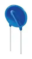


CV300K7BL1
TVS Varistor, 300 V, 385 V, CV, 775 V, Disc 7mm, Metal Oxide Varistor (MOV)
- Manufacturer: BOURNS
- Product type: TVS Varistors
- SVHC: No SVHC (04-Feb-2026)
- Product Range: CV
- Varistor Type: Metal Oxide Varistor (MOV)
- Voltage Rating VAC: 300V
- Voltage Rating VDC: 385V
- Varistor Case Style: Disc 7mm
- Clamping Voltage Vc Max: 775V
- Peak Energy (10/1000uS): 37J
- Operating Temperature Max: 85°C
- Operating Temperature Min: -40°C
- Peak Surge Current @ 8/20µs: 1.2kA
- Automotive Qualification Standard: -
| Delivery and price | |
|---|---|
| Units per pack | 1000 |
| Price | 0.124 € |
| Current stock | 1000+ |
| Lead time | 30 days |
## **Features**

**==> picture [34 x 20] intentionally omitted <==**

**----- Start of picture text -----**<br>
><br>CV 50 K20<br>**----- End of picture text -----**<br>


- n Formerly a                                product KEKOVAICON n Five model sizes available - 5, 7, 10, 14 and 20 mm

- n Broad range of current and energy handling capabilities

n 65 to 895 Vdc DC operating voltage range

   - n Available in tape and reel packaging for automatic pick-and-place

   - n RoHS compliant*

- n 50 to 680 Vrms AC voltage range; higher voltages available upon request (see the ZV Series for voltages below 50 V)

## **CV Series - Medium Voltage Disc Varistors**

## ~~**General Information**~~

The CV series of transient surge suppressors are disc shaped varistors designed to be operated continuously in low and medium voltage electronic system circuits as well as across AC power lines.

Due to their radial lead construction, these components require very little mounting space. They are available in five model sizes: 5 mm, 7 mm, 10 mm, 14 mm and 20 mm and feature a wide AC operating voltage ranging from 50 V to 680 V.

## ~~**Agency Recognition**~~

**==> picture [119 x 21] intentionally omitted <==**

**----- Start of picture text -----**<br>
|||
|---|---|
|Standard|UL 1449|
|File Number|E313168**|

**----- End of picture text -----**<br>


- ** Not all rated voltages are UL recognized; check the file for details.

## ~~**Varistor Symbol**~~

## ~~**Absolute Maximum Ratings**~~

**==> picture [318 x 167] intentionally omitted <==**

**----- Start of picture text -----**<br>
|||||
|---|---|---|---|
|Parameter|Value|Units|
|Continuous:|
|Steady State Applied Voltage|
|DC Voltage Range (Vdc)|65 to 895|V|
|AC Voltage Range (Vrms)|50 to 680|V|
|Transient:|
|Peak Single Pulse Surge Current, 8/20 µs Waveform (Imax)|400 to 6500|A|
|Single Pulse Surge Energy, 10/1000 µs Waveform (Wmax)|2.7 to 620|J|
|Operating Ambient Temperature|-40 to +85|°C|
|Storage Temperature Range|-40 to +125|°C|
|Threshold Voltage Temperature Coefficient|< +0.05|%/°C|
|Insulation Resistance|> 1|GW|
|Isolation Voltage Capability|>|2.5|kV|
|Response Time|< 25|ns|
|Climatic Category|40 / 85 / 56|

**----- End of picture text -----**<br>


**==> picture [8 x 9] intentionally omitted <==**

**----- Start of picture text -----**<br>
U<br>**----- End of picture text -----**<br>


## ~~**Index**~~

**==> picture [155 x 206] intentionally omitted <==**

**----- Start of picture text -----**<br>
|||
|---|---|
|Features ...................................................... 1|
|General Information ....................................|1|
|Agency Recognition ....................................|1|
|Varistor Symbol ...........................................|1|
|Absolute Maximum Ratings ........................|1|
|Device Ratings .........................................|2-3|
|Product Dimensions .................................|4-6|
|How to Order ...............................................|7|
|Typical Part Marking ...................................|7|
|Pulse Rating Curves ................................|7-9|
|Packaging Drawings .................................|10|
|11-12|
|Packaging Specifications  ....................|
|Assembly / Soldering|
|Recommendations for Through-Hole|
|Components ..............................................|13|
|Reliability Testing Procedures ..............|14-15|
|Terminology ...............................................|16|
|Legal Disclaimer........................................|17|

**----- End of picture text -----**<br>


Tel: +886-2 2562-4117 • Email: asiacus@bourns.com **Asia-Pacific: EMEA:** Tel: +36 88 885 877 • Email: eurocus@bourns.com

**The Americas:** Tel: +1-951 781-5500 • Email: americus@bourns.com **www.bourns.com**

**WARNING  Cancer and Reproductive Harm -** www.P65Warnings.ca.gov

- *RoHS Directive 2015/863, Mar 31, 2015 and Annex.

Specifications are subject to change without notice.

Users should verify actual device performance in their specific applications.

The products described herein and this document are subject to specific legal disclaimers as set forth on the last page of this document, and at www.bourns.com/docs/legal/disclaimer.pdf.

## **CV Series - Medium Voltage Disc Varistors3312 - 2 mm SMD Trimming Potentiometer**

## ~~**Device Ratings**~~

**==> picture [508 x 41] intentionally omitted <==**

**----- Start of picture text -----**<br>
Model Vrms Vdc @ 1 mAVn Vc Ic 10/1000 µsWmax max.P   8/20 µsImax @ 1 kHzC Typ.<br>V V V V A J W A pF<br>**----- End of picture text -----**<br>


|**Model**|**Vrms**|**Vdc**|**Vn**<br>**@ 1 mA**|**Vc**|**Ic**|**Wmax**<br>**10/1000 µs**|**P**<br>**max.**|**Imax**<br>**8/20 µs**|**C Typ.**<br>**@ 1 kHz**|
|---|---|---|---|---|---|---|---|---|---|
||V|V|V|V|A|J|W|A|pF|
|||||||||||
|CV 50 K 5|50|65|82|135|5|2.7|0.1|400|350|
|CV 50 K 7|50|65|82|135|10|6.8|0.25|1200|820|
|CV 50 K 10|50|65|82|135|25|17|0.4|2500|1400|
|CV 50 K 14|50|65|82|135|50|35|0.6|4500|2600|
|CV 50 K 20|50|65|82|135|100|75|1|6500|5000|
|CV 60 K 5|60|85|100|165|5|3|0.1|400|300|
|CV 60 K 7|60|85|100|165|10|7|0.25|1200|680|
|CV 60 K 10|60|85|100|165|25|16|0.4|2500|1200|
|CV 60 K 14|60|85|100|165|50|34|0.6|4500|2200|
|CV 60 K 20|60|85|100|165|100|71|1|6500|4100|
|CV 75 K 5|75|100|120|200|5|4|0.1|400|250|
|CV 75 K 7|75|100|120|200|10|9|0.25|1200|550|
|CV 75 K 10|75|100|120|200|25|21|0.4|2500|950|
|CV 75 K 14|75|100|120|200|50|41|0.6|4500|1800|
|CV 75 K 20|75|100|120|200|100|81|1|6500|3300|
|CV 95 K 5|95|125|150|250|5|6|0.1|400|200|
|CV 95 K 7|95|125|150|250|10|11|0.25|1200|440|
|CV 95 K 10|95|125|150|250|25|25|0.4|2500|750|
|CV 95 K 14|95|125|150|250|50|51|0.6|4500|1400|
|CV 95 K 20|95|125|150|250|100|106|1|6500|2600|
|CV 115 K 5|115|150|180|300|5|6|0.1|400|170|
|CV 115 K 7|115|150|180|300|10|13|0.25|1200|360|
|CV 115 K 10|115|150|180|300|25|30|0.4|2500|650|
|CV 115 K 14|115|150|180|300|50|62|0.6|4500|1200|
|CV 115 K 20|115|150|180|300|100|118|1|6500|2100|
|CV 130 K 5|130|170|205|340|5|7|0.1|400|150|
|CV 130 K 7|130|170|205|340|10|15|0.25|1200|320|
|CV 130 K 10|130|170|205|340|25|34|0.4|2500|580|
|CV 130 K 14|130|170|205|340|50|68|0.6|4500|1050|
|CV 130 K 20|130|170|205|340|100|142|1|6500|1900|
|CV 140 K 5|140|180|220|360|5|7|0.1|400|140|
|CV 140 K 7|140|180|220|360|10|18|0.25|1200|1200|
|CV 140 K 10|140|180|220|360|25|37|0.4|2500|2500|
|CV 140 K 14|140|180|220|360|50|75|0.6|4500|4500|
|CV 140 K 20|140|180|220|360|100|157|1|6500|6500|
|CV 150 K 5|150|200|240|395|5|9|0.1|400|130|
|CV 150 K 7|150|200|240|395|10|18|0.25|1200|280|
|CV 150 K 10|150|200|240|395|25|41|0.4|2500|510|
|CV 150 K 14|150|200|240|395|50|81|0.6|4500|900|
|CV 150 K 20|150|200|240|395|100|170|1|6500|1550|
|CV 175 K 5|175|225|270|455|5|9.5|0.1|400|120|
|CV 175 K 7|175|225|270|455|10|21|0.25|1200|250|
|CV 175 K 10|175|225|270|455|25|46|0.4|2500|440|
|CV 175 K 14|175|225|270|455|50|95|0.6|4500|800|
|CV 175 K 20|175|225|270|455|100|193|1|6500|1400|


Specifications are subject to change without notice.

Users should verify actual device performance in their specific applications.

_Continued on Next Page_

The products described herein and this document are subject to specific legal disclaimers as set forth on the last page of this document, and at www.bourns.com/docs/legal/disclaimer.pdf.

## **CDDFN5-0504N - TVS/Steering Diode ArrayCV Series - Medium Voltage Disc Varistors**

**==> picture [517 x 61] intentionally omitted <==**

**----- Start of picture text -----**<br>
Device Ratings (Continued)<br>Model Vrms Vdc @ 1 mAVn Vc Ic 10/1000 µsWmax max.P   8/20 µsImax @ 1 kHzC Typ.<br>V V V V A J W A pF<br>**----- End of picture text -----**<br>


||**Model**|**Vrms**|**Vdc**|**Vn**<br>**@ 1 mA**|**Vc**|**Ic**|**Wmax**<br>**10/1000 µs**|**P**<br>**max.**|**Imax**<br>**8/20 µs**|**C Typ.**<br>**@ 1 kHz**|**C Typ.**<br>**@ 1 kHz**|
|---|---|---|---|---|---|---|---|---|---|---|---|
|||V|V|V|V|A|J|W|A|pF||
|||||||||||||
||CV 230 K 5|230|300|360|595|5|13|0.1|400|90||
||CV 230 K 7|230|300|360|595|10|28|0.25|1200|190||
||CV 230 K 10|230|300|360|595|25|62|0.4|2500|350||
||CV 230 K 14|230|300|360|595|50|126|0.6|4500|650||
||CV 230 K 20|230|300|360|595|100|258|1|6500|1200||
||CV 250 K 5|250|320|390|650|5|14|0.1|400|80||
||CV 250 K 7|250|320|390|650|10|30|0.25|1200|180||
||CV 250 K 10|250|320|390|650|25|68|0.4|2500|320||
||CV 250 K 14|250|320|390|650|50|135|0.6|4500|580||
||CV 250 K 20|250|320|390|650|100|276|1|6500|1000||
||CV 275 K 5|275|350|430|710|5|16|0.1|400|70||
||CV 275 K 7|275|350|430|710|10|35|0.25|1200|160||
||CV 275 K 10|275|350|430|710|25|78|0.4|2500|300||
||CV 275 K 14|275|350|430|710|50|150|0.6|4500|530||
||CV 275 K 20|275|350|430|710|100|304|1|6500|900||
||CV 300 K 5|300|385|470|775|5|21|0.1|400|65||
||CV 300 K 7|300|385|470|775|10|37|0.25|1200|150||
||CV 300 K 10|300|385|470|775|25|82|0.4|2500|280||
||CV 300 K 14|300|385|470|775|50|169|0.6|4500|490||
||CV 300 K 20|300|385|470|775|100|350|1|6500|850||
||CV 320 K 10|320|420|510|840|25|91|0.4|2500|260||
||CV 320 K 14|320|420|510|840|50|184|0.6|4500|460||
||CV 320 K 20|320|420|510|840|100|388|1|6500|800||
||CV 385 K 10|385|505|620|1025|25|93|0.4|2500|240||
||CV 385 K 14|385|505|620|1025|50|193|0.6|4500|400||
||CV 385 K 20|385|505|620|1025|100|396|1|6500|700||
||CV 420 K 10|420|560|680|1120|25|97|0.4|2500|220||
||CV 420 K 14|420|560|680|1120|50|202|0.6|4500|350||
||CV 420 K 20|420|560|680|1120|100|418|1|6500|650||
||CV 460 K 10|460|615|750|1240|25|106|0.4|2500|200||
||CV 460 K 14|460|615|750|1240|50|220|0.6|4500|330||
||CV 460 K 20|460|615|750|1240|100|460|1|6500|550||
||CV 510 K 10|510|670|820|1355|25|115|0.4|2500|180||
||CV 510 K 14|510|670|820|1355|50|227|0.6|4500|310||
||CV 510 K 20|510|670|820|1355|100|478|1|6500|500||
||CV 550 K 10|550|745|910|1500|25|134|0.4|2500|170||
||CV 550 K 14|550|745|910|1500|50|264|0.6|4500|290||
||CV 550 K 20|550|745|910|1500|100|515|1|6500|450||
||CV 625 K 10|625|825|1000|1650|25|140|0.4|2500|160||
||CV 625 K 14|625|825|1000|1650|50|280|0.6|4500|270||
||CV 625 K 20|625|825|1000|1650|100|565|1|6500|400||
||CV 680 K 10|680|895|1100|1815|25|155|0.4|2500|150||
||CV 680 K 14|680|895|1100|1815|50|310|0.6|4500|250||
||CV 680 K 20|680|895|1100|1815|100|620|1|6500|350||


Specifications are subject to change without notice.

Users should verify actual device performance in their specific applications.

The products described herein and this document are subject to specific legal disclaimers as set forth on the last page of this document, and at www.bourns.com/docs/legal/disclaimer.pdf.

## **CV Series - Medium Voltage Disc Varistors3312 - 2 mm SMD Trimming Potentiometer**

## ~~**Product Dimensions**~~

**==> picture [512 x 523] intentionally omitted <==**

**----- Start of picture text -----**<br>
Dimension D t<br>Model<br>D  (Max.) t  (Max.) R d h  (Max.) a<br>CV 50 K 5 7  3.5 5 0.6 9.5 1.0<br>(.276) (.138) (.197) (.024) (.374) (.039)<br>CV 50 K 7 9 3.5 5 0.6 11.5 1.0 h<br>(.354) (.138) (.197) (.024) (.453) (.039)<br>CV 50 K 10 12.5 4.1 7.5 0.8 15 1.3<br>(.492) (.161) (.295) (.031) (.591) (.051)<br>CV 50 K 14 16.5 4.1 7.5 0.8 20 1.4<br>(.650) (.161) (.295) (.031) (.787) (.055)<br>CV 50 K 20 (22.5.886) (.1774.5 ) (.39410 ) (.0391.0 ) (1.02426 ) (.0631.6 ) (.118)3.0<br>MAX.<br>CV 60 K 5 (.2767  ) (.1383.5 ) (.1975 ) (.0240.6 ) (.3749.5 ) (.0431.1 ) 25.0<br>CV 60 K 7 9 3.5 5 0.6 11.5 1.1 (.984)MIN.<br>(.354) (.138) (.197) (.024) (.453) (.043)<br>CV 60 K 10 12.5 4.1 7.5 0.8 15 1.4<br>(.492) (.161) (.295) (.031) (.591) (.055)<br>CV 60 K 14 16.5 4.2 7.5 0.8 20 1.5<br>(.650) (.165) (.295) (.031) (.787) (.059)<br>CV 60 K 20 22.5 4.6 10 1.0 26 1.7<br>(.886) (.186) (.394) (.039) (1.024) (.067)<br>7  3.6 5 0.6 9.5 1.2<br>CV 75 K 5 R d<br>(.276) (.142) (.197) (.024) (.374) (.047)<br>CV 75 K 7 9 3.6 5 0.6 11.5 1.2 a<br>(.354) (.142) (.197) (.024) (.453) (.047)<br>CV 75 K 10 12.5 4.2 7.5 0.8 15 1.5<br>(.492) (.165) (.295) (.031) (.591) (.059)<br>CV 75 K 14 (16.5.650) (.1654.2 ) (.2957.5 ) (.0310.8 ) (.78720 ) (.0591.5 ) D t<br>CV 75 K 20 22.5 4.6 10 1.0 26 1.7<br>(.886) (.186) (.394) (.039) (1.024) (.067)<br>CV 95 K 5 7  3.8 5 0.6 9.5 1.4<br>(.276) (.150) (.197) (.024) (.374) (.055)<br>CV 95 K 7 9 3.8 5 0.6 11.5 1.4 h<br>(.354) (.150) (.197) (.024) (.453) (.055)<br>CV 95 K 10 12.5 4.3 7.5 0.8 15 1.7<br>(.492) (.169) (.295) (.031) (.591) (.067)<br>CV 95 K 14 16.5 4.3 7.5 0.8 20 1.7<br>(.650) (.169) (.295) (.031) (.787) (.067)<br>CV 95 K 20 (22.5.886) (.1864.6 ) (.39410 ) (.0391.0 ) (1.02426 ) (.0751.9 ) (.118)3.0<br>MAX.<br>CV 115 K 5 (.2767  ) (.1574.0 ) (.1975 ) (.0240.6 ) (.3749.5 ) (.0631.6 ) 25.0<br>CV 115 K 7 9 4.0 5 0.6 11.5 1.6 (.984)MIN.<br>(.354) (.157) (.197) (.024) (.453) (.063)<br>CV 115 K 10 12.5 4.3 7.5 0.8 15 1.9<br>(.492) (.169) (.295) (.031) (.591) (.075)<br>CV 115 K 14 16.5 4.4 7.5 0.8 20 1.9<br>(.650) (.173) (.295) (.031) (.787) (.075)<br>CV 115 K 20 22.5 4.8 10 1.0 26 2.1 R d<br>(.886) (.189) (.394) (.039) (1.024) (.083) a<br>CV 130 K 5 7  4.0 5 0.6 9.5 1.8<br>(.276) (.157) (.197) (.024) (.374) (.071)<br>CV 130 K 7 9 4.0 5 0.6 11.5 1.8<br>(.354) (.157) (.197) (.024) (.453) (.071)<br>CV 130 K 10 12.5 4.5 7.5 0.8 15 2.0<br>(.492) (.177) (.295) (.031) (.591) (.079)<br>CV 130 K 14 16.5 4.6 7.5 0.8 20 2.0<br>(.650) (.181) (.295) (.031) (.787) (.079)<br>CV 130 K 20 22.5 5.0 10 1.0 26 2.2<br>(.886) (.197) (.394) (.039) (1.024) (.087)<br>**----- End of picture text -----**<br>


MM DIMENSIONS: (INCHES)

Specifications are subject to change without notice. Users should verify actual device performance in their specific applications.

The products described herein and this document are subject to specific legal disclaimers as set forth on the last page of this document, and at www.bourns.com/docs/legal/disclaimer.pdf.

## **CDDFN5-0504N - TVS/Steering Diode ArrayCV Series - Medium Voltage Disc Varistors**

## ~~**Product Dimensions (Contiinued)**~~

**==> picture [512 x 523] intentionally omitted <==**

**----- Start of picture text -----**<br>
Dimension D t<br>Model<br>D  (Max.) t  (Max.) R d h  (Max.) a<br>CV 140 K 5 7  4.1 5 0.6 9.5 1.9<br>(.276) (.161) (.197) (.024) (.374) (.075)<br>CV 140 K 7 9 4.1 5 0.6 11.5 1.9 h<br>(.354) (.161) (.197) (.024) (.453) (.075)<br>CV 140 K 10 12.5 4.6 7.5 0.8 15 2.1<br>(.492) (.181) (.295) (.031) (.591) (.083)<br>CV 140 K 14 16.5 4.7 7.5 0.8 20 2.1<br>(.650) (.185) (.295) (.031) (.787) (.083)<br>CV 140 K 20 22.5 5.1 10 1.0 26 2.3 3.0<br>(.886) (.201) (.394) (.039) (1.024) (.091) (.118)<br>CV 150 K 5 (.2767  ) (.1694.3 ) (.1975 ) (.0240.6 ) (.3749.5 ) (.0792.0 ) MAX. 25.0<br>CV 150 K 7 (.3549 ) (.1694.3 ) (.1975 ) (.0240.6 ) (11.5.453) (.0792.0 ) (.984)MIN.<br>CV 150 K 10 12.5 4.6 7.5 0.8 15 2.2<br>(.492) (.181) (.295) (.031) (.591) (.087)<br>CV 150 K 14 16.5 4.8 7.5 0.8 20 2.2<br>(.650) (.189) (.295) (.031) (.787) (.087)<br>CV 150 K 20 22.5 5.2 10 1.0 26 2.4<br>(.886) (.205) (.394) (.039) (1.024) (.094)<br>CV 175 K 5 (.2767  ) (.1894.8 ) (.1975 ) (.0240.6 ) (.3749.5 ) (.0832.1 ) R d<br>CV 175 K 7 9 4.8 5 0.6 11.5 2.1 a<br>(.354) (.189) (.197) (.024) (.453) (.083)<br>CV 175 K 10 12.5 4.9 7.5 0.8 15 2.3<br>(.492) (.193) (.295) (.031) (.591) (.091)<br>CV 175 K 14 16.5 4.9 7.5 0.8 20 2.3<br>(.650) (.193) (.295) (.031) (.787) (.091) D t<br>CV 175 K 20 22.5 5.3 10 1.0 26 2.5<br>(.886) (.209) (.394) (.039) (1.024) (.098)<br>CV 230 K 5 7  4.8 5 0.6 9.5 2.6<br>(.276) (.189) (.197) (.024) (.374) (.102)<br>CV 230 K 7 9 4.8 5 0.6 11.5 2.6 h<br>(.354) (.189) (.197) (.024) (.453) (.102)<br>CV 230 K 10 12.5 5.4 7.5 0.8 15 2.8<br>(.492) (.213) (.295) (.031) (.591) (.110)<br>CV 230 K 14 16.5 5.5 7.5 0.8 20 2.8<br>(.650) (.217) (.295) (.031) (.787) (.110)<br>CV 230 K 20 22.5 5.9 10 1.0 26 3.0 3.0<br>(.886) (.1232) (.394) (.039) (1.024) (.118) (.118)<br>CV 250 K 5 (.2767  ) (.1975.0 ) (.1975 ) (.0240.6 ) (.3749.5 ) (.1102.8 ) MAX. 25.0<br>CV 250 K 7 (.3549 ) (.1975.0 ) (.1975 ) (.0240.6 ) (11.5.453) (.1102.8 ) (.984)MIN.<br>CV 250 K 10 12.5 5.6 7.5 0.8 15 3.0<br>(.492) (.220) (.295) (.031) (.591) (.118)<br>CV 250 K 14 16.5 5.7 7.5 0.8 20 3.0<br>(.650) (.224) (.295) (.031) (.787) (.118)<br>CV 250 K 20 22.5 6.1 10 1.0 26 3.2 R d<br>(.886) (.240) (.394) (.039) (1.024) (.126) a<br>CV 275 K 5 7  5.6 5 0.6 9.5 3.0<br>(.276) (.220) (.197) (.024) (.374) (.118)<br>CV 275 K 7 9 5.6 5 0.6 11.5 3.0<br>(.354) (.220) (.197) (.024) (.453) (.118)<br>CV 275 K 10 12.5 6.0 7.5 0.8 15 3.2<br>(.492) (.236) (.295) (.031) (.591) (.126)<br>CV 275 K 14 16.5 6.0 7.5 0.8 20 3.2<br>(.650) (.236) (.295) (.031) (.787) (.126)<br>CV 275 K 20 22.5 6.3 10 1.0 26 3.4<br>(.886) (.248) (.394) (.039) (1.024) (.134)<br>**----- End of picture text -----**<br>


MM DIMENSIONS: (INCHES)

Specifications are subject to change without notice. Users should verify actual device performance in their specific applications.

The products described herein and this document are subject to specific legal disclaimers as set forth on the last page of this document, and at www.bourns.com/docs/legal/disclaimer.pdf.

## **CV Series - Medium Voltage Disc Varistors3312 - 2 mm SMD Trimming Potentiometer**

## ~~**Product Dimensions (Contiinued)**~~

**==> picture [511 x 558] intentionally omitted <==**

**----- Start of picture text -----**<br>
Dimension D t<br>Model<br>D  (Max.) t  (Max.) R d h  (Max.) a<br>CV 300 K 5 7  5.8 5 0.6 9.5 3.2<br>(.276) (.228) (.197) (.024) (.374) (.126)<br>CV 300 K 7 9 5.8 5 0.6 11.5 3.2 h<br>(.354) (.228) (.197) (.024) (.453) (.126)<br>CV 300 K 10 12.5 6.1 7.5 0.8 15 3.4<br>(.492) (.240) (.295) (.031) (.591) (.134)<br>CV 300 K 14 16.5 6.1 7.5 0.8 20 3.4<br>(.650) (.240) (.295) (.031) (.787) (.134)<br>CV 300 K 20 22.5 6.6 10 1.0 26 3.6 3.0<br>(.886) (.260) (.394) (.039) (1.024) (.141) (.118)<br>CV 320 K 10 (12.5.492) (.2686.8 ) (.2957.5 ) (.0310.8 ) (.63016 ) (.1413.6 ) MAX. 25.0<br>CV 320 K 14 (16.5.650) (.2686.8 ) (.2957.5 ) (.0310.8 ) (.82721 ) (.1413.6 ) (.984)MIN.<br>CV 320 K 20 22.5 6.8 10 1.0 27 3.8<br>(.886) (.268) (.394) (.039) (1.063) (.150)<br>CV 385 K 10 12.5 7.4 7.5 0.8 16 4.2<br>(.492) (.291) (.295) (.031) (.630) (.165)<br>CV 385 K 14 16.5 7.4 7.5 0.8 21 4.2<br>(.650) (.291) (.295) (.031) (.827) (.165)<br>CV 385 K 20 (22.5.886) (.2957.5 ) (.39410 ) (.0391.0 ) (1.06327 ) (.1734.4 ) R d<br>CV 420 K 10 12.5 7.3 7.5 0.8 16 4.4 a<br>(.492) (.287) (.295) (.031) (.630) (.173)<br>CV 420 K 14 16.5 7.4 7.5 0.8 21 4.4<br>(.650) (.291) (.295) (.031) (.827) (.173)<br>CV 420 K 20 22.5 7.8 10 1.0 27 4.6<br>(.886) (.307) (.394) (.039) (1.063) (.181) D t<br>CV 460 K 10 12.5 7.8 7.5 0.8 16 4.8<br>(.492) (.307) (.295) (.031) (.630) (.189)<br>CV 460 K 14 16.5 7.8 7.5 0.8 21 4.8<br>(.650) (.307) (.295) (.031) (.827) (.189)<br>CV 460 K 20 22.5 8.2 10 1.0 27 5.0 h<br>(.886) (.323) (.394) (.039) (1.063) (.197)<br>CV 510 K 10 12.5 8.2 7.5 0.8 16 5.1<br>(.492) (.323) (.295) (.031) (.630) (.201)<br>CV 510 K 14 16.5 8.2 7.5 0.8 21 5.1<br>(.650) (.323) (.295) (.031) (.827) (.201)<br>CV 510 K 20 22.5 8.7 10 1.0 27 5.3 3.0<br>(.886) (.343) (.394) (.039) (1.063) (.209) (.118)<br>CV 550 K 10 (12.5.492) (.3468.8 ) (.2957.5 ) (.0310.8 ) (.63016 ) (.2205.6 ) MAX. 25.0<br>CV 550 K 14 (16.5.650) (.3468.8 ) (.2957.5 ) (.0310.8 ) (.82721 ) (.2205.6 ) (.984)MIN.<br>CV 550 K 20 22.5 9.2 10 1.0 27 5.8<br>(.886) (.362) (.394) (.039) (1.063) (.228)<br>CV 625 K 10 12.5 9.1 7.5 0.8 16 6.1<br>(.492) (.358) (.295) (.031) (.630) (.240)<br>CV 625 K 14 16.5 9.2 7.5 0.8 21 6.1 R d<br>(.650) (.362) (.295) (.031) (.827) (.240) a<br>CV 625 K 20 22.5 9.7 10 1.0 27 6.3<br>(.886) (.382) (.394) (.039) (1.063) (.248)<br>CV 680 K 10 12.5 9.7 7.5 0.8 16 6.6 Typical Part Marking<br>(.492) (.382) (.295) (.031) (.630) (.260)<br>CV 680 K 14 (1.6506.5) (.3869.8 ) (.2957.5 ) (.0310.8 ) (.82721 ) (.2606.6 ) MANUFACTURER’STRADEMARK<br>CV 680 K 20 (22.5.886) (10.2.402) (.39410 ) (.0391.0 ) (1.06327 ) (.2686.8 ) MODELSERIES Vrms<br>MODEL SIZE<br>DIMENSIONS: (INCHES)MM TOLERANCEVn  CV 50 K 20<br>**----- End of picture text -----**<br>


Specifications are subject to change without notice. Users should verify actual device performance in their specific applications.

The products described herein and this document are subject to specific legal disclaimers as set forth on the last page of this document, and at www.bourns.com/docs/legal/disclaimer.pdf.

## **CV Series - Medium Voltage Disc Varistors3312 - 2 mm SMD Trimming Potentiometer**

## ~~**How to Order**~~

**C V 1 3 0 K 1 4 R L 1 y y**

Series Designator CV = CV Series Max. Continuous Operating Voltage (Vrms) Vn Tolerance K = ±10 % Model Size 5 = 5 mm 14 = 14 mm 7 = 7 mm 20 = 20 mm 10 = 10 mm Packaging R = Reel* B = Bulk A = Ammo Pack (Available only upon special request)* _*Reel and Ammo Pack options not available for Model Size 20._ Lead Style L1 =  Straight Leads L5 =  Crimped Leads Special Parameters YY = Unique two digit suffix is assigned to each customer requesting special parameters. Please contact Bourns for more information.

## **Instructions for Creating Orderable Part Number:**

- 1) Start with base part number in characteristics table

   - (example: CV130K14).

- 2)  Add Packaging: R

(example part number becomes CV130K14R).

- 3)  Add Lead Style: L1

(example part number becomes CV130K14RL1).

- 4) Part number can have no spaces or lower case letters.

~~**Pulse Rating Curves -** Protection level with worst-case condition in the tolerance region~~

## **Model Size 5 - (CV50 ~ CV275)**

**==> picture [489 x 254] intentionally omitted <==**

**----- Start of picture text -----**<br>
4000<br>2000<br>1000<br>800 10 [4]<br>5<br>600 300<br>275 250<br>230 10 [3]<br>400<br>5<br>300<br>275<br>200 10 [2]<br>5<br>95<br>75<br>60 50 10 [1]<br>100 95 75 5<br>80<br>60 50 10 [0]<br>60 5<br>40 10 [-1]<br>10 [-5] 10 [-4] 10 [-3] 10 [-2] 10 [-1] 10 [0] 10 [1] 10 [2] 10 [3] 10 [4] 10 [1] 5 10 [2] 5 10 [3] 5 10 [4]<br>I (Amps) tp (µs)<br>175<br>150<br>130<br>140<br>6<br>5 10<br>10<br>10 4<br>250<br>230 175 115<br>150 140<br>130 115<br>3 10<br>2<br>10<br>10<br>2<br>1x<br>8<br>V (Volts)<br> (Amps)<br>Imax<br>**----- End of picture text -----**<br>


Specifications are subject to change without notice.

Users should verify actual device performance in their specific applications.

The products described herein and this document are subject to specific legal disclaimers as set forth on the last page of this document, and at www.bourns.com/docs/legal/disclaimer.pdf.

## **CV Series - Medium Voltage Disc Vari3312 - 2 mm SMD Trimming Pot** ~~**entiometer**~~ **stors**

~~**Pulse Rating Curves (Continued) -** Protection level with worst-case condition in the tolerance region~~

## **Model Size 7 - (CV50 ~ CV300)**

**==> picture [489 x 250] intentionally omitted <==**

**----- Start of picture text -----**<br>
4000<br>2000<br>1000<br>10 [4]<br>800<br>5<br>600<br>10 [3]<br>400 300 5<br>115 10 [2]<br>200 175<br>5<br>150 95<br>75<br>10 [1]<br>60<br>100 95 75 5<br>50<br>80<br>60 50 10 [0]<br>60 5<br>40 10 [-1]<br>10 [-5] 10 [-4] 10 [-3] 10 [-2] 10 [-1] 10 [0] 10 [1] 10 [2] 10 [3] 10 [4] 10 [1] 5 10 [2] 5 10 [3] 5 10 [4]<br>I (Amps) tp (µs)<br>300<br>275<br>230<br>175<br>150<br>130<br>4<br>10 6<br>140<br>5<br>3<br>10 10<br>10<br>250<br>250<br>140<br>115<br>10<br>2<br>10<br>1x<br>2<br>275<br>230<br>130 8<br>V (Volts)<br> (Amps)<br>Imax<br>**----- End of picture text -----**<br>


## **Model Size 10 - (CV50 ~ CV680)**

**==> picture [498 x 256] intentionally omitted <==**

**----- Start of picture text -----**<br>
4000<br>2000<br>1000<br>10 [4]<br>800<br>5<br>600<br>10 [3]<br>400 5<br>10 [2]<br>200<br>95 5<br>75<br>95 60 10 [1]<br>5<br>100<br>80 75 60<br>10 [0]<br>60 50 5<br>40 10 [-1]<br>10 [-5] 10 [-4] 10 [-3] 10 [-2] 10 [-1] 10 [0] 10 [1] 10 [2] 10 [3] 10 [4] 10 [1] 5 10 [2] 5 10 [3] 5 10 [4]<br>I (Amps) tp (µs)<br>106<br>140<br>175 150<br>115 105<br>104<br>250<br>130<br>150<br>130<br>50<br>550 320<br>680<br>625 550<br>680 510 460<br>550 420 385<br>460 300<br>385<br>320<br>275<br>230<br>275<br>230 103<br>102<br>10<br>1x<br>2<br>140<br>175<br>115<br>625<br>510<br>420<br>300<br>250<br>8<br>V (Volts)<br> (Amps)<br>Imax<br>**----- End of picture text -----**<br>


Specifications are subject to change without notice.

Users should verify actual device performance in their specific applications. The products described herein and this document are subject to specific legal disclaimers as set forth on the last page of this document, and at www.bourns.com/docs/legal/disclaimer.pdf.

## **CV Series - Medium Voltage Disc Varistors3312 - 2 mm SMD Trimming Potentiometer**

~~**Pulse Rating Curves (Continued) -** Protection level with worst-case condition in the tolerance region~~

## **Model Size 14 - (CV50 ~ CV680)**

**==> picture [205 x 254] intentionally omitted <==**

**----- Start of picture text -----**<br>
4000<br>2000<br>1000<br>800<br>600<br>400 385855 320200<br>200<br>955<br>755<br>955 600<br>100 500<br>80 755 600<br>60 500<br>40<br>10 [[-5]] 10 [[-4]] 10 [[-3]] 10 [[-2]] 10 [[-1]] 10 [[0]] 10 [[1]] 10 [[2]] 10 [[3]] 10 [[4]]<br>I (Amps)<br>680<br>625<br>680<br>550 510<br>460600 420200<br>385855<br>320200<br>300000 275755<br>250500 230300<br>275755 175755 150500<br>140400 130300<br>115155<br>550500 510100<br>420200<br>230300<br>150500<br>130300<br>625255<br>140400<br>460600<br>300000<br>175755<br>250500<br>115155<br>V (Volts)<br>**----- End of picture text -----**<br>


**==> picture [506 x 471] intentionally omitted <==**

**----- Start of picture text -----**<br>
10 [4]<br>800<br>5<br>600<br>10 [3]<br>400 385855 320200 5<br>10 [2]<br>200<br>5<br>955<br>755 10 [1]<br>955 600<br>5<br>100 500<br>80 755 600<br>10 [0]<br>60 500 5<br>10 [-1]<br>40<br>10 [[-5]] 10 [[-4]] 10 [[-3]] 10 [[-2]] 10 [[-1]] 10 [[0]] 10 [[1]] 10 [[2]] 10 [[3]] 10 [[4]] 10 [1] 5 10 [2] 5 10 [3] 5 10 [4]<br>I (Amps) tp (µs)<br>Model Size 20 - (CV50 ~ CV680)<br>4000<br>2000<br>1000<br>800 420 10 [4]<br>320 5<br>600<br>10 [3]<br>400<br>5<br>200 10 [2]<br>95 5<br>75<br>95 60 10 [1]<br>100 50 5<br>80 75 60<br>10 [0]<br>60 5<br>50<br>40 10 [-1]<br>10 [-5] 10 [-4] 10 [-3] 10 [-2] 10 [-1] 10 [0] 10 [1] 10 [2] 10 [3] 10 [4] 10 [1] 5 10 [2] 5 10 [3] 5 10 [4]<br>I (Amps) tp (µs)<br>385<br>460600 420200<br>385855<br>320200<br>300000 275755<br>250500 230300<br>275755 175755 150500<br>140400 130300<br>115155<br>680<br>625<br>680<br>550<br>460<br>300 275<br>250 230<br>175 150<br>140 130<br>150 115<br>510<br>106<br>106<br>105<br>105<br>4<br>104<br>103<br>550500 510100<br>420200<br>230300<br>150500<br>130300<br>625255<br>320<br>230<br>175<br>130<br>625<br>103<br>102<br>102<br>10<br>10<br>1x<br>2<br>10<br>2<br>1x<br>140400<br>460600<br>300000<br>175755<br>550 510<br>460 420<br>385<br>300 275<br>250<br>140<br>250500<br>115155<br>115<br>8<br>8<br>V (Volts)<br> (Amps)<br>Imax<br>V (Volts)<br> (Amps)<br>Imax<br>**----- End of picture text -----**<br>


Specifications are subject to change without notice.

Users should verify actual device performance in their specific applications.

The products described herein and this document are subject to specific legal disclaimers as set forth on the last page of this document, and at www.bourns.com/docs/legal/disclaimer.pdf.

## **CDDFN5-0504N - TVS/Steering Diode ArrayCV Series - Medium Voltage Disc Varistors3312 - 2 mm SMD Trimming Potentiometer**

## ~~**Packaging Specifcations - Tape**~~

Conforms to IES Publication 286-2 Ed. 3: 2008-03

## **Dimension R = 5 mm**

**==> picture [356 x 100] intentionally omitted <==**

**----- Start of picture text -----**<br>
ΔP ΔP<br>Δh Δh<br>W1<br>H0<br>H1 D0 H1 W2<br>W<br>H<br>L P1 d R W0<br>L1 P0 P<br>T t<br>Dimensions on Next Page<br>**----- End of picture text -----**<br>


## **Dimension R = 7.5 mm & 10 mm**

**==> picture [505 x 349] intentionally omitted <==**

**----- Start of picture text -----**<br>
Δh Δh ΔP ΔP<br>H1 H1<br>W1<br>H0<br>W2<br>H D0<br>W<br>L<br>P1 d R W0<br>L1 P0 P T t<br>Dimensions on Next Page<br>Reel  Ammo Pack (Available upon Special Request)<br>18<br>(.709) 265<br>85 DIA. (10.433)<br>DIA.<br>(3.346)<br>300<br>(11.811)<br>DIA.<br>47<br>(1.850) [MAX.]<br>(2.165)55 MAX. DIMENSIONS: (INCHES)MM<br>295<br>(11.614)<br>55<br>(2.165)<br>**----- End of picture text -----**<br>


Specifications are subject to change without notice.

Users should verify actual device performance in their specific applications. The products described herein and this document are subject to specific legal disclaimers as set forth on the last page of this document, and at www.bourns.com/docs/legal/disclaimer.pdf.

## **CV Series - Medium Voltage Disc Varistors3312 - 2 mm SMD Trimming Potentiometer**

## ~~**Packaging Specifcations - Tape (Continued)**~~

**==> picture [504 x 38] intentionally omitted <==**

**----- Start of picture text -----**<br>
Model Size<br>Symbol Parameter<br>5 7 10 14 20<br>18 +1.0/-0.5<br>**----- End of picture text -----**<br>


|**Symbol**|**Parameter**|**Model Size**|**Model Size**|**Model Size**|**Model Size**|**Model Size**|**Model Size**|**Model Size**|**Model Size**|**Model Size**|**Model Size**|**Model Size**|**Model Size**|**Model Size**|**Model Size**|
|---|---|---|---|---|---|---|---|---|---|---|---|---|---|---|---|
|||**5**|||**7**||**10**|||||**14**||**20**||
|||18+1.0/-0.5||||||||||||||
|W|Carrier tape width|||||||(.709 +.039/-.020)||||||||
|W0|Hold down tape width|||||||5MIN.<br>(.197)...........||||||||
|W1|Sprocket hole position|||||||9+0.75/-0.5<br>(.354 +.030/-.020)||||||||
|W2|Distance between the upper edges of the<br>carrier tape and hold down tape||||||||3 <br>(.118). .|MAX.<br>.........||||||
|T|Total tape thickness|||1.5MA<br>(.059). .....||X.<br>....||||1.7     MAX.<br>(.067). .........|||||1.9MAX.<br>(.075). .........|
|t|Tape thickness||||||||0.9<br>(.035). .|MAX.<br>.........||||||
|P|Pitch of component|||||12.7 ± 1.0<br>(.500 ± .039)|||||||25.4 ±||1.0<br>.039)|
||||||||||||||(1.000 ±|||
|P0|Feed hole pitch||||||||12.7 ±|0.3<br>.012)||||||
||||||||||(.500 ±|||||||
|P1|Feed hole center to pitch|||3.85±0.|||||||8.95± 0.7<br>(.352 ± .028)||||7.7 ± 0.7<br>(.303 ± .028)|
|R|Lead spacing||||||||||||||10 +0.5/-0.2<br>(.394 +.020/-.008)|
|DP|Component alignment||||||||±1.3|MAX.<br>..........||||||
||||||||||<br>(±.051).|||||||
|Dh|Component alignment||||||||±2|MAX.<br>.........||||||
||||||||||<br>(±.079).|||||||
|d|Wire diameter||0.6MAX.<br>(.024). .........|||||||0.8MAX.<br>(.031). ........|||||1     MAX.<br>(.039). ........|
|D0|Feed hold diameter||||||||4 ± 0|.2<br>.008)||||||
||||||||||(.157 ±|||||||
|H|Height from tape center to component base||||||||18 +2.0|||||||
|H0|Seating plane height||||||||16 ± 0.5<br>(.630 ± .020)|||||||
|H1|Component height||32.2MAX.<br>(1.268). ........||||||46.5M<br>(1.831). ...||||AX.<br>.....|||
|L|Protrusion - cut out||||||||11    MAX.<br>(.433). ........|||||||
|L1|Protrusion - cut off||||||||0.5    MAX.<br>(.020). ........|||||||


MM DIMENSIONS: (INCHES)

Specifications are subject to change without notice. Users should verify actual device performance in their specific applications.

The products described herein and this document are subject to specific legal disclaimers as set forth on the last page of this document, and at www.bourns.com/docs/legal/disclaimer.pdf.

## **CDDFN5-0504N - TVS/Steering Diode ArrayCV Series - Medium Voltage Disc Varistors3312 - 2 mm SMD Trimming Potentiometer**

## ~~**Packaging Quantities - Bulk**~~

**==> picture [506 x 32] intentionally omitted <==**

**----- Start of picture text -----**<br>
Model Size<br>Voltage<br>5 7 10 14 20<br>**----- End of picture text -----**<br>


|**Voltage**|**Model Size**|**Model Size**|**Model Size**|**Model Size**|**Model Size**|
|---|---|---|---|---|---|
||**5**|**7**|**10**|**14**|**20**|
|||||||
|50|1500|1500|600|400|300|
|60|1500|1500|600|400|300|
|75|1500|1500|600|400|300|
|95|1500|1000|600|400|300|
|115|1500|1000|500|400|300|
|130|1500|1000|500|400|300|
|140|1500|1000|500|400|300|
|150|1500|1000|500|400|300|
|175|1500|1000|500|400|300|
|230|1000|1000|500|300|300|
|250|1000|1000|500|300|200|
|275|1000|1000|500|300|200|
|300|1000|1000|500|300|200|
|320|||500|300|200|
|385|||400|300|200|
|420|||400|300|200|
|460|||400|300|200|
|510|||400|300|200|
|550-680|||300|300|200|


## ~~**Packaging Quantities - Reel**~~

**==> picture [506 x 33] intentionally omitted <==**

**----- Start of picture text -----**<br>
Model Size<br>Voltage<br>5 7 10 14 20<br>**----- End of picture text -----**<br>


|**Voltage**|**Model Size**|**Model Size**|**Model Size**|**Model Size**|**Model Size**|
|---|---|---|---|---|---|
||**5**|**7**|**10**|**14**|**20**|
|||||||
|50|1500|1500|1300|700||
|60|1500|1500|1300|700||
|75|1500|1500|1300|700||
|95|1500|1000|1300|600||
|115|1300|1000|1000|600||
|130|1300|1000|1000|600||
|140|1200|1000|1000|600||
|150|1200|1000|1000|600||
|175|1200|1000|1000|500||
|230|1000|1000|1000|500||
|250|1000|1000|800|400||
|275|1000|1000|800|400||
|300|900|1000|800|400||
|320|||800|400||
|385|||700|400||
|420|||700|300||
|460|||600|300||
|510|||600|300||
|550-680|||600|300||


Specifications are subject to change without notice.

Users should verify actual device performance in their specific applications. The products described herein and this document are subject to specific legal disclaimers as set forth on the last page of this document, and at www.bourns.com/docs/legal/disclaimer.pdf.

## **3312 - 2 mm SMD Trimming PotentiometerCV Series - Medium Voltage Disc Varistors**

## ~~**Assembly Recommendations for Through-Hole Components**~~

**==> picture [91 x 128] intentionally omitted <==**

**----- Start of picture text -----**<br>
POINT TO BE FIXED<br>2<br>(.079)<br>/ -<br>on<br>MM<br>DIMENSIONS:<br>(INCHES)<br>**----- End of picture text -----**<br>


Very often before soldering through-hole components, their leads get bent. It is important not to damage the components during lead bending. Damage most commonly incurred during bending is cracks in epoxy parts, which can lead to increased humidity sensitivity of a component and, consequentially, a shorter lifetime.

In order to avoid epoxy damage, it is necessary to:

- fix the most sensitive point (epoxy parts) of a component body

- bend the wire at least 2 mm below the end of epoxy parts

Other potential damage to a component which can lead to component failure or a shorter lifetime is thermal shock during manual soldering with a soldering iron. This can occur when a soldering iron is placed too close to one point of the component body and it happens most often when the solder joint is too close to the varistor body.

## **Resistance to Soldering Heat**

In the case of automatic wave soldering, it is important to provide sufficient resistance to soldering heat. In order to prevent any potential problems, internal standards were introduced for testing the resistance to soldering heat of through-hole components: 300 °C, 10 seconds.

## **Pb-free Wave Soldering Profile Recommendations**

Recommended soldering profiles for all above components are in accordance with JEDEC standard curves (J-STD-020D) and are, therefore, compatible with the Pb-free process.

**Lead-free Wave Soldering Profile -** Pb-free wave profile requirements for soldering heat resistance of components

**==> picture [207 x 125] intentionally omitted <==**

**----- Start of picture text -----**<br>
T3 t(w1+w2)<br>Tmerit<br>MELTING POINT 217 °C<br>T2<br>T1<br>t1 TIME<br>TEMPERATURE<br>**----- End of picture text -----**<br>


|**Parameter**|**Symbol**|**Specification**|
|---|---|---|
|Preheating temperature gradient||**ecification**<br>4 °C/sec. max.|
|Preheating time|t1|2 to 5 min.|
|Min. preheating temperature|T1|130 °C|
|Max. preheating temperature|T2|180 °C|
|Melting temperature/point|Tmeltv|217 °C|
|Time in wave soldering phase<br>(w1+w2)|tw1+w2|10 sec.|
|Max. wave temperature (w1+w2)|Ts|265 °C +0/-5 °C|
|Cooling temperature gradient||6° C/sec. max.|
|Temperature jump from T2 to T3<br>(w1)|T3(w1) - T2|120 °C max|
|Time from 25 °C to T3 (wave<br>temperature)||8 min. max.|


Specifications are subject to change without notice.

Users should verify actual device performance in their specific applications.

The products described herein and this document are subject to specific legal disclaimers as set forth on the last page of this document, and at www.bourns.com/docs/legal/disclaimer.pdf.

## **CDDFN5-0504N - TVS/Steering Diode ArrayCV Series - Medium Voltage Disc Varistors**

## ~~**Reliability Testing Procedures**~~

Varistor test procedures comply with CECC 42200, IEC 1051-1/2 (and AEC-Q200, if applicable). Test results are available upon customer request. Special tests can be performed upon customer request.

**==> picture [505 x 35] intentionally omitted <==**

**----- Start of picture text -----**<br>
Condition to be<br>Reliability Parameter Test Tested According to Satisfied after<br>Testing<br>**----- End of picture text -----**<br>


|**Reliability Parameter**|**Test**|**Tested According to**|**Condition to be**<br>**Satisfed after**<br>**Testing**|
|---|---|---|---|
|||||
|**AC/DC Bias Reliability**|AC/DC Life Test|CECC 42200, Test 4.20 or<br>IEC 1051-1, Test 4.20,<br>AEC-Q200 Test 8 - 1000 h at UCT||δVn (1 mA)| < 10 %|
|**Pulse Current Capability**|Imax 8/20 µs|CECC 42200, Test C 2.1 or<br>IEC 1051-1, Test 4.5<br>10 pulses in the same direction at<br>2pulsesper minute at maximumpeak current for 10pulses||δVn (1 mA)| < 10 %<br>no visible damage|
|**Pulse Energy Capability**|Wmax 10/1000 µs|CECC 42200, Test C 2.1 or<br>IEC 1051-1, Test 4.5<br>10 pulses in the same direction at<br>1 pulse every 2 minutes at maximum peak current for 10<br>pulses||δVn (1 mA)| < 10 %<br>no visible damage|
|**WLD Capability**|WLD x 10|ISO 7637, Test pulse 5, 10 pulses at rate of 1 per minute||δVn (1 mA)| < 15 %<br>no visible damage|
|**Vjump Capability**|Vjump 5 min.|Increase of supply voltage to V ≥ Vjump for 1 minute||δVn (1 mA)| < 15 %<br>no visible damage|
|**Environmental and**<br>**Storage Reliability**|Climatic Sequence|CECC 42200, Test 4.16 or<br>IEC 1051-1, Test 4.17<br>a) Dry heat, 16h, UCT, Test Ba, IEC 68-2-2<br>b) Damp heat, cyclic, the frst cycle: 55 °C, 93 % RH, 24 h,<br>Test Db 68-2-4<br>c) Cold, LCT, 2 h, Test Aa, IEC 68-2-1<br>d) Damp heat cyclic, remaining 5 cycles: 55 °C, 93 % RH,<br>24 h/cycle, Test Bd, IEC 68-2-30||δVn (1 mA)| < 10 %|
||Thermal Shock|CECC 42200, Test 4.12, Test Na, IEC 68-2-14,<br>AEC-Q200 Test 16,5||δVn (1 mA)| < 10 %<br>no visible damage|
||Steady State<br>Damp Heat|CECC 42200, Test 4.17, Test Ca, IEC 68-2-3,<br>AEC-Q200 Test 6, 56 days, 40 °C, 93 % RH,<br>AEC-Q200 Test 7: Bias,Rh,T all at 85.||δVn (1 mA)| < 10 %|
||Storage Test|IEC 68-2-2, Test Ba, AEC-Q200 Test 3, 1000 h at maximum<br>storage temperature||δVn (1 mA)| < 5 %|


_Continued on Next Page_

Specifications are subject to change without notice. Users should verify actual device performance in their specific applications.

The products described herein and this document are subject to specific legal disclaimers as set forth on the last page of this document, and at www.bourns.com/docs/legal/disclaimer.pdf.

## **3312 - 2 mm SMD Trimming PotentiometerCV Series - Medium Voltage Disc Varistors3312 - 2 mm SMD Trimming Potentiometer**

## ~~**Reliability Testing Procedures (Continued)**~~

**==> picture [506 x 35] intentionally omitted <==**

**----- Start of picture text -----**<br>
Condition to be<br>Reliability Parameter Test Tested According to Satisfied after<br>Testing<br>**----- End of picture text -----**<br>


|**Reliability Parameter**|**Test**|**Tested According to**|**Condition to be**<br>**Satisfed after**<br>**Testing**|
|---|---|---|---|
|||||
|**Mechanical Reliability**|Solderability|CECC 42200, Test 4.10.1, Test Ta, IEC 68-2-20 solder bath<br>and refow method|Solderable at<br>shipment and after<br>2 years of storage,<br>criteria:  >95% must<br>be covered by solder<br>for refow meniscus|
||Resistance to<br>SolderingHeat|CECC 42200, Test 4.10.2, Test Tb, IEC 68-2-20 solder bath<br>nad refow method|<br>|δVn (1 mA)| < 5 %|
||Terminal Strength|<br>JIS-C-6429, App. 1, 18N for 60 sec. - same for AEC-Q200<br>Test 22|No visual damage|
||Board Flex|JIS-C-6429, App. 2, 2 mm min.<br>AEC-Q200 test 21 - Board fex: 2 mm fex min.||δVn (1 mA)| < 2 %<br>No visible damage|
||Vibration|<br>CECC 42200, Test 4.15, Test Fc, IEC 68-2-6,<br>AEC-Q200 Test 14<br>Frequency range 10 to 55 Hz (AEC: 10-2000 Hz)<br>Amplitude 0.75 m/s2or 98 m/s2(AEC: 5 g for 20 minutes) To-<br>tal duration 6 h (3x2 h) (AEC: 12 cycles each of 3 directions)<br>Waveshape - half sine||δVn (1 mA)| < 2 %<br>No visible damage|
||Mechanical Shock|CECC 42200, Test 4.14, Test Ea, IEC 68-2-27, AEC-Q200<br>Test 13.<br>Acceleration = 490 m/s2(AEC: MIL-STD-202-Method 213),<br>Pulse duration = 11 ms,<br>Waveshape - half sine;Number of shocks = 3x6||δVn (1 mA)| < 10 %<br>No visible damage|
|**Electrical Transient**<br>**Conduction**|ISO-7637-1 Pulses|AEC-Q200 Test 30: Test pulses 1 to 3.<br>Also otherpulses - freestyle.||δVn (1 mA)| < 10 %<br>No visible damage|


Specifications are subject to change without notice. Users should verify actual device performance in their specific applications.

The products described herein and this document are subject to specific legal disclaimers as set forth on the last page of this document, and at www.bourns.com/docs/legal/disclaimer.pdf.

## **CDDFN5-0504N - TVS/Steering Diode ArrayCV Series - Medium Voltage Disc Varistors**

## ~~**Terminology**~~

|**Term**<br>**Symbol**<br>**Definition**|
|---|
|rms<br>RatedAC Voltage .......eeeeeeeeeeeMo<br>teeeesteeeseeeee Maximum continuous sinusoidalAC voltage (<5% total harmonic distortion) which may be|
|dc<br>Rated DC Voltage......eeeeeeM0 eeeeeseseees Maximum continuous DC voltage (<5% ripple) which may be applied to the component|
|Supply Voltage... cesses Visesessssesseeeeee The voltage by which the system is designated and to which certain operating|
|rms|
|dc<br>dcand at +25 °C or at any other specified<br>Leakage Current...eee<br>ceeeeseeeeeeee**e**<br>h<br>Current passing through the varistor atV|
|n<br>n)<br>Varistor Voltage ......eeMocesses WVOltage across the varistor measured at a given reference current (I|
|n<br>Reference Current...... eee) ceseeeeeeeeeeReference current=<br>1mADC|
|Clamping Voltage .........................Vc......................The peak voltage developed across the varistor under standard atmospheric conditions,|
|Protection Level<br>when passing an 8/20 µs class current pulse|
|c<br>ClassCurrent... cceeeeeseesseeeeeA peak value of current which is 1/10 of the maximum peak current for 100 pulses at two|
|c/Vapp<br>Voltage Clamping Ratio...............V<br>sissusseeA figure of merit measure of the varistor clamping effectiveness as defined by the symbols|
|c<br>app<br>app<br>rms<br>dc|
|jump<br>Jump Start Transient ..........0..V<br>sists<br>Dejump Starttransient results from the temporary application of an overvoltage in excess|
|overvoltage condition due to the voltage regulation failing or it may be deliberately generated|
|when it becomes necessary to boost start the car.|
|Rated Single Pulse .......................Wmax.................Energy which may be dissipated for a single 10/1000 µs pulse of a maximum rated|
|Transient Energy<br>current, with rated AC voltage or rated DC voltage also applied, without causing device|
|failure|
|Load Dump Transient..................WLD..................Load Dump is a transient which occurs in automotive environments. It is an exponentially|
|nator is still generating charging current with other loads remaining on the alternator circuit|
|at the time of battery disconnect.|
|Rated Peak Single Pulse ..............Imax...................Maximum peak current which may be applied for a single 8/20 µs pulse, with rated line|
|Transient Current<br>voltage also applied, without causing device failure|
|Rated Transient Average ..............P ........................Maximum average power which may be dissipated due to a group of pulses occurring<br>Power Dissipation<br>within a specified isolated time period, without causing device failure at 25 °C|
|Capacitance...<br>cece eee:OueeesieseseesesCapacitance between two terminals ofthe varistor measured @ 1 kHz|
|α<br>nand I1as<br>Non-linearity Exponent...<br>eieeeeeeeeeee-A measure of varistor nonlinearity between two given operating currents,<br>||
|- k is a device constant,|
|- I1< I < Inand|
|- a log (I1/In)/log(V1/Vn) = 1/log (V1/Vn), where:|
|- Iris reference current (1 mA) and Vnis varistor voltage|
|- I1= 10 In, V1is the voltage measured at I1|


Varistor Voltage Temperature .......TC .....................(VCoefficient n @ 85 °C - Vn @ 25 °C) / (Vn @ 25 °C) x 60 °C) x 100

DHD = Dump Heat Test Duration

REV. E 06/20

Specifications are subject to change without notice. Users should verify actual device performance in their specific applications. The products described herein and this document are subject to specific legal disclaimers as set forth on the last page of this document, and at www.bourns.com/docs/legal/disclaimer.pdf.

## **Legal Disclaimer Notice**

This legal disclaimer applies to purchasers and users of Bourns[®] products manufactured by or on behalf of Bourns, Inc. and its affiliates (collectively, “Bourns”).

Unless otherwise expressly indicated in writing, Bourns[®] products and data sheets relating thereto are subject to change without notice.  Users should check for and obtain the latest relevant information and verify that such information is current and complete before placing orders for Bourns[®] products.

The characteristics and parameters of a Bourns[®] product set forth in its data sheet are based on laboratory conditions, and statements regarding the suitability of products for certain types of applications are based on Bourns’ knowledge of typical requirements in generic applications.  The characteristics and parameters of a Bourns[®] product in a user application may vary from the data sheet characteristics and parameters due to (i) the combination of the Bourns[®] product with other components in the user’s application, or (ii) the environment of the user application itself.  The characteristics and parameters of a Bourns[®] product also can and do vary in different applications and actual performance may vary over time.  Users should always verify the actual performance of the Bourns[®] product in their specific devices and applications, and make their own independent judgments regarding the amount of additional test margin to design into their device or application to compensate for differences between laboratory and real world conditions.

Unless Bourns has explicitly designated an individual Bourns[®] product as meeting the requirements of a particular industry standard (e.g., ISO/TS 16949) or a particular qualification (e.g., UL listed or recognized), Bourns is not responsible for any failure of an individual Bourns[®] product to meet the requirements of such industry standard or particular qualification.  Users of Bourns[®] products are responsible for ensuring compliance with safety-related requirements and standards applicable to their devices or applications.

Bourns[®] products are not recommended, authorized or intended for use in nuclear, lifesaving, life-critical or life-sustaining applications, nor in any other applications where failure or malfunction may result in personal injury, death, or severe property or environmental damage.  Unless expressly and specifically approved in writing by two authorized Bourns representatives on a case-by-case basis, use of any Bourns[®] products in such unauthorized applications might not be safe and thus is at the user’s sole risk.  Life-critical applications include devices identified by the U.S. Food and Drug Administration as Class III devices and generally equivalent classifications outside of the United States.

Bourns expressly identifies those Bourns[®] standard products that are suitable for use in automotive applications on such products’ data sheets in the section entitled “Applications.”  Unless expressly and specifically approved in writing by two authorized Bourns representatives on a case-by-case basis, use of any other Bourns[®] standard products in an automotive application might not be safe and thus is not recommended, authorized or intended and is at the user’s sole risk.  If Bourns expressly identifies a sub-category of automotive application in the data sheet for its standard products (such as infotainment or lighting), such identification means that Bourns has reviewed its standard product and has determined that if such Bourns[®] standard product is considered for potential use in automotive applications, it should only be used in such sub-category of automotive applications.  Any reference to Bourns[®] standard product in the data sheet as compliant with the AEC-Q standard or “automotive grade” does not by itself mean that Bourns has approved such product for use in an automotive application.

Bourns[®] standard products are not tested to comply with United States Federal Aviation Administration standards generally or any other generally equivalent governmental organization standard applicable to products designed or manufactured for use in aircraft or space applications. Bourns expressly identifies Bourns[®] standard products that are suitable for use in aircraft or space applications on such products’ data sheets in the section entitled “Applications.”  Unless expressly and specifically approved in writing by two authorized Bourns representatives on a case-by-case basis, use of any other Bourns[®] standard product in an aircraft or space application might not be safe and thus is not recommended, authorized or intended and is at the user’s sole risk.

The use and level of testing applicable to Bourns[®] custom products shall be negotiated on a case-by-case basis by Bourns and the user for which such Bourns[®] custom products are specially designed.  Absent a written agreement between Bourns and the user regarding the use and level of such testing, the above provisions applicable to Bourns[®] standard products shall also apply to such Bourns[®] custom products.

Users shall not sell, transfer, export or re-export any Bourns[®] products or technology for use in activities which involve the design, development, production, use or stockpiling of nuclear, chemical or biological weapons or missiles, nor shall they use Bourns[®] products or technology in any facility which engages in activities relating to such devices.  The foregoing restrictions apply to all uses and applications that violate national or international prohibitions, including embargos or international regulations.  Further, Bourns[®] products and Bourns technology and technical data may not under any circumstance be exported or re-exported to countries subject to international sanctions or embargoes.  Bourns[®] products may not, without prior authorization from Bourns and/or the U.S. Government, be resold, transferred, or re-exported to any party not eligible to receive U.S. commodities, software, and technical data.

To the maximum extent permitted by applicable law, Bourns disclaims (i) any and all liability for special, punitive, consequential, incidental or indirect damages or lost revenues or lost profits, and (ii) any and all implied warranties, including implied warranties of fitness for particular purpose, non-infringement and merchantability.

_For your convenience, copies of this Legal Disclaimer Notice with German, Spanish, Japanese, Traditional Chinese and Simplified Chinese bilingual versions are available at:_

_Web Page: http://www.bourns.com/legal/disclaimers-terms-and-policies_

_PDF: http://www.bourns.com/docs/Legal/disclaimer.pdf_

C1753 05/17/18R
Updated at June 6, 2026
Bourns, Inc. is a globally recognized manufacturer of high-reliability electronic components, headquartered in Riverside, California. Renowned for its engineering excellence, the company delivers critical solutions across a diverse range of demanding markets, including automotive, industrial, consumer electronics, telecommunications, and medical equipment. The Bourns product portfolio is anchored by an industry-leading selection of passive components and circuit protection devices. The brand is particularly dominant in magnetic components, offering thousands of high-performance power inductors, alongside specialized RF and toroidal inductors engineered for optimized power management and signal integrity. Equally prominent is their comprehensive suite of circuit protection solutions. This robust lineup features a vast array of standard and resettable fuses, transient voltage suppressors (including TVS varistors and diodes), and gas discharge tubes (GDTs) designed to rigorously safeguard sensitive electronics against overvoltage and overcurrent faults. Beyond its core passives and protection technologies, Bourns manufactures highly effective EMC and RFI suppression components, such as common mode chokes and power line filters. The company's offering also extends into discrete semiconductors and power management, including Schottky diodes, fast recovery rectifiers, bridge rectifiers, and board-level transformers. This expansive breadth of quality components provides design engineers with a trusted foundation for developing resilient, efficient, and long-lasting electronic systems.
About Novapart
Novapart is a B2B electronic component broker specialising in stock shortages and cost reduction. We source hard-to-find parts and identify compliant alternatives across a catalogue of 410,000+ components from 500+ manufacturers.
Learn more →Stock Shortage Specialist
When a component is unavailable, discontinued or has an unacceptable lead time, we tap into our network of vetted European and Asian distributors to source what you need — without compromising on quality or traceability.
Request a quote →Compliant Alternatives
We identify pin-to-pin, electrically equivalent substitutes that meet the same certifications (RoHS, AEC-Q100, REACH) as your original specification — validated against datasheets, not just part numbers. Often at a lower cost.
BOM Analysis service →