
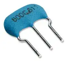


CSTLS3M52G56-B0
Resonator, CSTLS_G Series, 3.52 MHz, ± 0.5%, ± 0.2%, 50 ohm
- Manufacturer: MURATA
- Product type: Resonators
- SVHC: Lead titanium zirconium oxide (04-Feb-2026)
- Frequency: 3.52MHz
- No. of Pins: 3Pins
- Product Range: CSTLS_G Series
- Resonant Frequency: 3.52MHz
- Resonant Impedance: 50ohm
- Frequency Stability: ± 0.2%
- Frequency Tolerance: ± 0.5%
- Oscillator Mounting: Through Hole
- Operating Temperature Max: 80°C
- Operating Temperature Min: -20°C
| Delivery and price | |
|---|---|
| Units per pack | 500 |
| Price | 0.042 € |
| Current stock | 10+ |
| Lead time | 30 days |
P17E.pdf 2015.12.25

## Ceramic Resonators (CERALOCK[®] ) Application Manual

P17E.pdf 2015.12.25

Note • Please read rating and CAUTION (for storage, operating, rating, soldering, mounting and handling) in this catalog to prevent smoking and/or burning, etc. • This catalog has only typical specifications. Therefore, please approve our product specifications or transact the approval sheet for product specifications before ordering.

## **Introduction**

Ceramic resonators (CERALOCK[®] ) are made of high stability piezoelectric ceramics that function as a mechanical resonator.

This device has been developed to function as a reference signal generator and the frequency is primarily adjusted by the size and thickness of the ceramic element.

With the advance of the IC technology, various equipment may be controlled by a single LSI integrated circuit, such as the one-chip microprocessor.

CERALOCK[®] can be used as the timing element in most microprocessor based equipment.

In the future, more and more applications will use CERALOCK[®] because of its high stability nonadjustment performance, miniature size and cost savings. Typical applications include TVs, VCRs, automotive electronic devices, telephones, copiers, cameras, voice synthesizers, communication equipment, remote controls and toys.

This manual describes CERALOCK[®] and will assist you in applying it effectively.

- * CERALOCK[®] is the brand name of these MURATA products.

## **EU RoHS Compliant**

- All the products in this catalog comply with EU RoHS.

- EU RoHS is "the European Directive 2011/65/EU on the Restriction of the Use of Certain Hazardous Substances in Electrical and Electronic Equipment."

- For more details, please refer to our website 'Murata's Approach for EU RoHS'

- (http://www.murata.com/eneu/support/compliance/rohs).

P17E.pdf 2015.12.25

Note • Please read rating and CAUTION (for storage, operating, rating, soldering, mounting and handling) in this catalog to prevent smoking and/or burning, etc. • This catalog has only typical specifications. Therefore, please approve our product specifications or transact the approval sheet for product specifications before ordering.

1

2

3

4

5

6

7

8

## **Contents**

Product specifications are as of December 2015.

|**Characteristics and Types of CERALOCK®**<br>1. General Characteristics of CERALOCK®……<br>**1**|p2|
|---|---|
|2. Types of CERALOCK®……………………………|p3|
|MHz Band lead CERALOCK® (CSTLS Series)………………|p3|
|MHz Band Chip CERALOCK®||
|(CSACW/CSTCC/CSTCR/CSTCE/CSTCW Series)…………|p4|
|**Principles of CERALOCK®**<br>1. Equivalent Circuit Constants……………………<br>**2**|p6|
|2. Basic Oscillation Circuits………………………|p9|
|**Specifications of CERALOCK®**<br>1. Electrical Specifications…………………………<br> <br>**3**|p12|
|Electrical Specifications of MHz Band Lead CERALOCK®||
|(CSTLS Series)……………………………………………<br>|p12|
|Electrical Specifications of MHz Band Chip CERALOCK®||
|(CSACW Series) (CSTCC/CSTCR/CSTCE/CSTCW Series)…<br>|p14|
|2. Mechanical and Environmental||
|Specifications of CERALOCK®……………………<br>|p15|
|**Applications of Typical Oscillation Circuits**<br>**4**||
|1. Cautions for Designing Oscillation Circuits…<br>|p17|
|2. Application to Various Oscillation Circuits…<br>|p18|
|Application to C-MOS Inverter……………………<br>|p18|
|Application to H-CMOS Inverter…………………<br>|p19|
|**Characteristics of CERALOCK® Oscillation Circuits**<br>**5**||
|1. Stability of Oscillation Frequency……………<br>|p20|
|2. Characteristics of the Oscillation Level………<br>|p21|
|3. Characteristics of Oscillation Rise Time……<br>|p22|
|4. Starting Voltage……………………………………<br>|p23|
|**Application Circuits to Various ICs/LSIs**<br>1. Application to Microcomputers………………<br> <br>**6**|p24|
|2. Application to Remote Control ICs……………<br>|p27|
|3. Application to ICs for Office Equipment……<br>|p27|
|4. Other Kinds of Applications to Various ICs…<br>|p27|
|**Notice**…………………………………………………<br> <br>**7**|p28|
|**Appendix**<br>**Equivalent Circuit Constants of CERALOCK®**……<br>**8**|p29|


Please check the MURATA website (http://www.murata.com/) if you cannot find the part number in the catalog.

P17E.pdf 2015.12.25

Note • Please read rating and CAUTION (for storage, operating, rating, soldering, mounting and handling) in this catalog to prevent smoking and/or burning, etc. • This catalog has only typical specifications. Therefore, please approve our product specifications or transact the approval sheet for product specifications before ordering.

1

## ® 1 Characteristics and Types of CERALOCK

**==> picture [31 x 52] intentionally omitted <==**

**----- Start of picture text -----**<br>
RoHS<br>**----- End of picture text -----**<br>


## **1. General Characteristics of CERALOCK[®]**

Ceramic resonators use the mechanical resonance of piezoelectric ceramics. (Generally, lead zirconium titanate: PZT.)

The oscillation mode varies with resonant frequency. The table on the right shows this relationship.

As a resonator device, Crystal Unit is well-known. RC oscillation circuits and LC oscillation circuits are also used to produce electrical resonance. The following are the characteristics of CERALOCK[®] .

- ① High stability of oscillation frequency:

- Oscillation frequency stability is between that of Crystal Units and LC or RC oscillation circuits.

- The temperature coefficient of Crystal Units is 10–6/ °C maximum and approximately 10–3 to 10–4/°C for LC or RC oscillation circuits. For comparison these, it is 10–5/°C at –20 to +80°C for ceramic resonators.

- ② Small configuration and light weight:

- The ceramic resonator is half the size of popular Crystal Units.

## Vibration Mode and Frequency Range

**==> picture [240 x 220] intentionally omitted <==**

**----- Start of picture text -----**<br>
Frequency (Hz)  1k 10k 100k 1M 10M 100M 1G<br>Vibration Mode<br>1<br>Flexural<br>mode<br>2<br>Length<br>mode<br>3<br>Area<br>expansion<br>mode<br>4<br>Radius<br>vibration<br>5<br>Shear<br>thickness<br>mode<br>6<br>Thickness<br>expansion<br>mode<br>7<br>Surface<br>acoustic<br>wave<br>**----- End of picture text -----**<br>


**==> picture [139 x 8] intentionally omitted <==**

**----- Start of picture text -----**<br>
[Note] : ←→show the direction of vibration<br>**----- End of picture text -----**<br>


- ③ Low price, non-adjustment:

- CERALOCK[®] is mass produced, resulting in low cost and high stability.

- Unlike RC or LC circuits, ceramic resonators use mechanical resonance. This means it is not basically affected by external circuits or by the fluctuation of the supply voltage.

- Highly stable oscillation circuits can therefore be made without the need of adjustment.

The table briefly describes the characteristics of various oscillator elements.

## Characteristics of Various Oscillator Elements

**==> picture [241 x 201] intentionally omitted <==**

**----- Start of picture text -----**<br>
Oscillation  Long-<br>Name Symbol Price Size Adjust-ment Frequency Initial  term<br>Tolerance Stability<br>lower<br>LC Big Required ±2.0% Fair<br>cost<br>lower<br>CR Small Required ±2.0% Fair<br>cost<br>Crystal Expen- Not  ±<br>Big Excellent<br>Unit sive required 0.001%<br>Ceramic Inexpen- Small Not  ±0.5% Excellent<br>Resonator sive required<br>**----- End of picture text -----**<br>


2

P17E.pdf 2015.12.25

Note • Please read rating and CAUTION (for storage, operating, rating, soldering, mounting and handling) in this catalog to prevent smoking and/or burning, etc. • This catalog has only typical specifications. Therefore, please approve our product specifications or transact the approval sheet for product specifications before ordering.

1

## 2. Types of CERALOCK®

## **MHz Band lead CERALOCK[®] (CSTLS Series)**

As CSTLS series does not require externally mounted capacitors, the number of components can be reduced, allowing circuits to be made more compact.

The table shows the frequency range and appearance of the three-terminal CERALOCK[®] with built-in load capacitance.

Part Numbering (Ex.) **CS T LS 4M00 G 5 3 -A0** I **❶ ❷ ❸ ❹ ❺** ❻ ❼ ❽ ❾ ❶Product ID IL ILIL JULI

❷Frequency/Built-in Capacitance

❸Structure/Size

Part Numbers and Dimensions of  lead CERALOCK[®] (CSTLS Series)

**==> picture [222 x 179] intentionally omitted <==**

**----- Start of picture text -----**<br>
Part Number Frequency Dimensions (in mm)<br>CSTLS G 3.40–10.00MHz<br>- ~<br>*<br>16.00–<br>CSTLS X<br>70.00MHz<br>°<br>* 16.00-32.99MHz : 3.5<br>2.5 2.5<br>8.0<br>5.5<br>2.5 2.5<br>3.0<br>3.0<br>5.5<br>3.5<br>6.5<br>3.5<br>**----- End of picture text -----**<br>


LS: Round Lead Type

❹Nominal Center Frequency

❺Type

G: Thickness Shear vibration,

X: Thickness Longitudinal Vibration (3rd overtone)

❻Frequency Tolerance

1: ±0.1%, 2: ±0.2%, 3: ±0.3%, 5: ±0.5%, D: DTMF,

Z: Others

❼Built-in Load capacitance

1: 5pF, 3: 15pF, 4: 22pF, 5: 30pF, 6: 47pF

❽Individual Specification

With standard products, "❽ Individual Specification" is omitted, and "❾ Package Specification Code" is carried up.

❾Packaging

–B0: Bulk,

–A0: Radial Taping H0=18mm Ammo Pack (Standard)

3

P17E.pdf 2015.12.25

Note • Please read rating and CAUTION (for storage, operating, rating, soldering, mounting and handling) in this catalog to prevent smoking and/or burning, etc. • This catalog has only typical specifications. Therefore, please approve our product specifications or transact the approval sheet for product specifications before ordering.

1

## **MHz Band Chip CERALOCK[®] (CSACW/CSTCC/ CSTCR/CSTCE/CSTCW Series)**

The MHz band Chip CERALOCK[®] has a wide frequency range and small footprint to meet further downsizing and highdensity mounting requirements.

The table shows the dimensions and two-terminals standard land patterns of the CERALOCK[®] CSACW series.

The second table shows the dimensions and three-terminals standard land patterns of CSTCC/CSTCR/CSTCE/CSTCW series chip resonator (built-in load capacitance type.) The carrier tape dimensions of CSTCR series are shown on the next page.

## Dimensions and Standard Land Pattern of Chip CERALOCK[®] (CSACW Series)

**==> picture [232 x 109] intentionally omitted <==**

**----- Start of picture text -----**<br>
Dimensions<br>Part Number Frequency (MHz) Standard Land Pattern (in mm)<br>0.5 0.5<br>CSACW X *2 20.01–70.00<br>| i<br>2.0<br>2.0 2.5<br>1.0<br>0.8 0.3<br>2.0±0.2<br>0.8 0.3<br>**----- End of picture text -----**<br>


- *1 Thickness varies with frequency.

- *2  Conformal coating or washing of the components is not acceptable because they are not heretically sealed.

**==> picture [227 x 44] intentionally omitted <==**

**----- Start of picture text -----**<br>
Part Numbering<br>(Ex.) CS T CR 4M00 G 5 3 -R0<br>PLL<br>❶ ❷ ❸ ❹ ❺ ❻ ❼ ❽ ❾<br>**----- End of picture text -----**<br>


❶Product ID

- ❷Frequency/No capacitance built-in

A: No Capacitance Built-in, T: Built-in Capacitance

❸Structure/Size

CC/CR/CE/CN/CM: Cap Chip Type, CW: Monolithic Chip Type

❹Nominal Center Frequency

❺Type

G: Thickness Shear Vibration,

- V: Thickness Longitudinal Vibration,

X: Thickness Longitudinal Vibration (3rd overtone)

❻Frequency Tolerance

1: ±0.1%, 2: ±0.2%, 3: ±0.3%, 5: ±0.5%, Z: Others

❼Load Capacitance Value

(In case of CSACW, CSACN and CSACM value is for external capacitance of standard circuit)

- 1: 5pF or 6pF, 2 : 10pF, 3: 15pF, 5: 33pF or 39pF,

- 6: 47pF

❽Individual Specification

With standard products, "❽ Individual Specification" is omitted, and "❾ Package Specification Code" is carried up.

❾Packaging

- –B0: Bulk, –R0: Plastic Taping φ180mm Reel Package

4

P17E.pdf 2015.12.25

Note • Please read rating and CAUTION (for storage, operating, rating, soldering, mounting and handling) in this catalog to prevent smoking and/or burning, etc. • This catalog has only typical specifications. Therefore, please approve our product specifications or transact the approval sheet for product specifications before ordering.

1

## Dimensions and Standard Land Pattern of Chip CERALOCK® (CSTCC/CSTCR/CSTCE/CSTCW Series)

## Dimensions of Carrier Tape for Chip CERALOCK[®]

**==> picture [504 x 498] intentionally omitted <==**

**----- Start of picture text -----**<br>
||||||||||
|---|---|---|---|---|---|---|---|---|
|CSTCR Series|
|Dimensions|
|Part Number|Frequency (MHz)|Standard Land Pattern (in mm)|4.0±0.1|2.0±0.05|ø1.5|[+0.1]|-0|
|*1|
|CSTCC|G|*2|2.00–3.99|1.2|1.2|1.4|1.2|1.2|
|4.0±0.1|ø1.5|[+0.1]|-0|
|The cover film peel strength force 0.1 to 0.7N|2.2±0.1|(3˚)|
|2.5|2.5|The cover film peel speed 300mm/min.|Cover Film|
|10˚|
|re|faa|
|>|
|Direction of Feed|(in mm)|
|0.8|0.7|0.8|0.7|0.8|
|CSTCC|_|G|*2|4.00–7.99|ert|
|0.4|0.4|0.4|
|1.5|1.5|
|mee|
|:|
|&|
|0.4|0.8|0.4|0.8|0.4|
|CSTCC|G|*2|8.00–13.99|
|1.2|1.2|
|m|e|et|
|0.3|0.65|0.3|0.65|0.3|
|CSTCE|:|V|*2|14.00–20.00|
|0.95|0.95|
|*1|
|0.5|0.5|0.5|0.5|0.5|
|CSTCW|X|*2|20.01–70.00|
|1.0|1.0|

**----- End of picture text -----**<br>


- *1 Thickness varies with frequency.

- *2  Conformal coating or washing of the components is not acceptable because they are not hermetically sealed.

5

P17E.pdf 2015.12.25

Note • Please read rating and CAUTION (for storage, operating, rating, soldering, mounting and handling) in this catalog to prevent smoking and/or burning, etc. • This catalog has only typical specifications. Therefore, please approve our product specifications or transact the approval sheet for product specifications before ordering.

2 Principles of CERALOCK[®]

2

**==> picture [31 x 52] intentionally omitted <==**

**----- Start of picture text -----**<br>
RoHS<br>**----- End of picture text -----**<br>


## **1. Equivalent Circuit Constants**

Fig. 2-1 shows the symbol for a ceramic resonator. The impedance and phase characteristics measured between the terminals are shown in Fig. 2-2. This illustrates that the resonator becomes inductive in the frequency zone between the frequency Fr (resonant frequency), which provides the minimum impedance, and the frequency Fa (anti-resonant frequency), which provides the maximum impedance.

It becomes capacitive in other frequency zones. This means that the mechanical vibration of a two-terminal resonator can be replaced equivalently with a combination of series and parallel resonant circuits consisting of an inductor : L, a capacitor : C, and a resistor : R. In the vicinity of the specific frequency (Refer to Note 1 on page 8), the equivalent circuit can be expressed as shown in Fig. 2-3.

Fr and Fa frequencies are determined by the piezoelectric ceramic material and the physical parameters. The equivalent circuit constants can be determined from the following formulas. (Refer to Note 2 on page 8)

|Fr=1/2π    L1C1<br>Fa=1/2π    L1C1C0/(C1+C0)=Fr   1+C1/C0<br>Qm=1/2πFrC1R1<br>(Qm : Mechanical Q)||(2-1)<br>(2-2)<br>(2-3)|
|---|---|---|
||||


Considering the limited frequency range of Fr≦F≦Fa, the impedance is given as Z=Re+jωLe (Le≧0) as shown in Fig. 2-4, and CERALOCK[®] should work as an inductance Le (H) having the loss Re (Ω).

**==> picture [239 x 86] intentionally omitted <==**

**----- Start of picture text -----**<br>
Symbol<br>Impedance between Two Terminals Z=R+jx<br>(R : Real Component, X : Impedance Component)<br>Phase φ =tan [-1] X/R<br>**----- End of picture text -----**<br>


Fig. 2-1 Symbol for the Two-Terminal CERALOCK[®]

**==> picture [239 x 230] intentionally omitted <==**

**----- Start of picture text -----**<br>
10 [5]<br>10 [4]<br>10 [3]<br>10 [2]<br>10<br>Fr Fa Frequency (kHz)<br>90<br>0<br>-90<br>**----- End of picture text -----**<br>


Fig. 2-2 Impedance and Phase Characteristics of CERALOCK[®]

**==> picture [239 x 226] intentionally omitted <==**

**----- Start of picture text -----**<br>
L1 C1 R1<br>C0<br>R [1]  : Equivalent Resistance<br>L [1]  : Equivalent Inductance<br>C [1]  : Equivalent Capacitance<br>C [0]  : Parallel Equivalent Capacitance<br>Fig. 2-3 Electrical Equivalent Circuit of CERALOCK [®]<br>Re Le<br>Re : Effective Resistance<br>Le : Effective Inductance<br>**----- End of picture text -----**<br>


Fig. 2-4 Equivalent Circuit of CERALOCK[®] in the Frequency Band Fr≦F≦Fa

6

P17E.pdf 2015.12.25

Note • Please read rating and CAUTION (for storage, operating, rating, soldering, mounting and handling) in this catalog to prevent smoking and/or burning, etc. • This catalog has only typical specifications. Therefore, please approve our product specifications or transact the approval sheet for product specifications before ordering.

2

The table on this page shows a comparison of the equivalent constants between CERALOCK[®] and Crystal Units.

In comparison, there is a large difference in capacitance and Qm, which results in the difference of oscillating conditions, when actually operated.

The table in the appendix shows the standard values of an equivalent circuit constant for each type of CERALOCK[®] . Furthermore, other higher harmonic modes exist, other than the desired oscillation mode. These other oscillation modes exist because the ceramic resonator uses mechanical resonance.

Fig. 2-5 shows those characteristics.

**==> picture [239 x 222] intentionally omitted <==**

**----- Start of picture text -----**<br>
CSTLS4M00G53–B0<br>1M<br>Main Vibration<br>100k<br>10k  3rd Vibration<br>1k<br>100<br>10<br>1<br>0 10 20 30 40<br>Frequency (MHz)<br>Impedance [Z] (Ω)<br>**----- End of picture text -----**<br>


Fig. 2-5 Spurious Characteristics of CERALOCK[®]

## Comparison of Equivalent Circuits of CERALOCK[®] and Crystal Unit (Reference)

**==> picture [511 x 96] intentionally omitted <==**

**----- Start of picture text -----**<br>
Oscillation<br>Resonator L1 (μH) C1 (pF) C0 (pF) R1 (Ω) Qm dF (kHz)<br>Frequency<br> 2.00MHz 1.71×10 [3] 4 20.8 43.9    475 177.2<br>CERALOCK [®]  4.00MHz 0.46×10 [3] 3.8 19.8   9   1220 350.9<br> 8.00MHz 0.13×10 [3] 3.5 19.9   8    775 641.6<br>2.457MHz 7.20×10 [5] 0.005  2.39 37 298869 3<br>Crystal Unit  4.00MHz 2.10×10 [5] 0.007  2.39 22.1 240986 6<br> 8.00MHz 1.80×10 [5] 0.002  4.48 154.7  59600 2<br>**----- End of picture text -----**<br>


7

P17E.pdf 2015.12.25

Note • Please read rating and CAUTION (for storage, operating, rating, soldering, mounting and handling) in this catalog to prevent smoking and/or burning, etc. • This catalog has only typical specifications. Therefore, please approve our product specifications or transact the approval sheet for product specifications before ordering.

2

## **Notes**

## **(Note 1)**

The relationship between the size of the resonator and the resonant frequency is described as follows. For example, the frequency doubles if the thickness doubles, when thickness vibration is used.

The following relationship is obtained when the length of the resonators is ℓ, the resonance frequency is Fr, the speed of sound waves travelling through piezoelectric ceramics, and the wavelength is λ.

Fr・ℓ = Const.

(frequency constant, Fr・t for the thickness) λ = 2ℓ

**==> picture [82 x 8] intentionally omitted <==**

As seen in the above formula, the frequency constant determines the size of the resonator.

## **(Note 2)**

In Fig. 2-3, when resistance R1 is omitted for simplification, the impedance Z (ω) between two terminals is expressed by the following formula.

**==> picture [135 x 116] intentionally omitted <==**

**==> picture [184 x 22] intentionally omitted <==**

**==> picture [103 x 9] intentionally omitted <==**

**==> picture [486 x 171] intentionally omitted <==**

**----- Start of picture text -----**<br>
1<br>Fr = ωr/2π =<br>2π    L1C1<br>ℓ=λ/2<br>1 C1<br>Fa = ωa/2π=  = Fr    1+<br>2π    C0C1L1/(C0+C1) C0<br>Amplitude<br>Range of<br>StandingWave L1 C1<br>(Min.Amplitude) (Max.Amplitude)<br>C0<br>Fig.Ⅰ Fig. Ⅱ<br>**----- End of picture text -----**<br>


8

P17E.pdf 2015.12.25

Note • Please read rating and CAUTION (for storage, operating, rating, soldering, mounting and handling) in this catalog to prevent smoking and/or burning, etc. • This catalog has only typical specifications. Therefore, please approve our product specifications or transact the approval sheet for product specifications before ordering.

2

## **2. Basic Oscillation Circuits**

Generally, basic oscillation circuits can be grouped into the following 3 categories.

① Use of positive feedback

② Use of negative resistance element

③ Use of delay in transfer time or phase

In the case of ceramic resonators, Crystal Units, and LC oscillators, positive feedback is the circuit of choice.

Among the positive feedback oscillation circuit using an LC, the tuning type anti-coupling oscillation circuit, Colpitts and Hartley circuits are typically used. See Fig. 2-6.

In Fig. 2-6, a transistor, which is the most basic amplifier, is used.

The oscillation frequencies are approximately the same as the resonance frequency of the circuit consisting of L, CL1 and CL2 in the Colpitts circuit or consisting of L1, L2 and C in the Hartley circuit. These frequencies can be represented by the following formulas. (Refer to Note 3 on page 11.)

(Colpitts Circuit) 1 fosc. = 2π L・ CL1 · CL2 (2-4) CL1 + CL2 (Hartley Circuit) 1 fosc. = (2-5) 2π C(L1 + L2)

**==> picture [239 x 120] intentionally omitted <==**

**----- Start of picture text -----**<br>
CL1 CL2 L1 L2<br>L C<br>Colpitts Circuit  Hartley Circuit<br>**----- End of picture text -----**<br>


Fig. 2-6 Basic Configuration of LC Oscillation Circuit

**==> picture [239 x 171] intentionally omitted <==**

**----- Start of picture text -----**<br>
Amplifier<br>Mu Factor : α<br>Phase Shif : θ1<br>Feedback Circuit<br>Feedback Ratio : β<br>Phase Shif : θ2<br>Oscillation Conditions<br>Loop Gain G = α·β≧1<br>Phase Shift θ = θ1+ θ2 = 360°×n<br>**----- End of picture text -----**<br>


Fig. 2-7 Principle of Oscillation

In an LC network, the inductor is replaced by a ceramic resonator, taking advantage of the fact that the resonator becomes inductive between resonant and anti-resonant frequencies.

This is most commonly used in the Colpitts circuit.

The operating principle of these oscillation circuits can be seen in Fig. 2-7. Oscillation occurs when the following conditions are satisfied.

**==> picture [230 x 35] intentionally omitted <==**

In Colpitts circuit, an inverter of θ1 = 180° is used, and it is inverted more than θ2 = 180° with L and C in the feedback circuit. The operation with a ceramic resonator can be considered the same.

9

P17E.pdf 2015.12.25

Note • Please read rating and CAUTION (for storage, operating, rating, soldering, mounting and handling) in this catalog to prevent smoking and/or burning, etc. • This catalog has only typical specifications. Therefore, please approve our product specifications or transact the approval sheet for product specifications before ordering.

2

It is common and simple to utilize an inverter for the Colpitts circuit with CERALOCK[®] .

Fig. 2-8 shows the basic oscillation circuit with inverter.

In an open loop circuit by cutting at point Ⓐ, it is possible to measure loop gain G and phase shift θ.

Fig. 2-9 shows the actual measuring circuit, and an example of the measuring result is shown in Fig. 2-10.

**==> picture [239 x 142] intentionally omitted <==**

**----- Start of picture text -----**<br>
α(θ1)<br>Rf<br>A<br>CERALOCK [®]<br>CL1 CL2<br>β(θ2)<br>**----- End of picture text -----**<br>


Fig. 2-8 Basic Oscillation Circuit with Inverters

**==> picture [239 x 503] intentionally omitted <==**

**----- Start of picture text -----**<br>
α(θ1) β(θ2)<br>IC CERALOCK [®]<br>Zin1MΩ//8pF<br>Z0=50Ω Rf Vector<br>C2 C1 Volt<br>Vin Meter<br>S.S.G<br>Loop Gain  : G= α · β<br>Phase Shift  :  θ1+ θ2<br>Fig. 2-9 Measuring Circuit Network of Loop Gain and Phase<br>Shift<br>40 180<br>30 Phase<br>(Oscillation)<br>20 90<br>Gain<br>10<br>0 0<br>-10<br>-20 -90 CERALOCK [®]<br>CSTLS4M00G53–B0<br>VDD=+5V<br>-30 CL1=CL2=15pF<br>IC : TC4069UBP<br>-40 -180 (TOSHIBA)<br>3.80 3.90 4.00 4.10 4.20<br>Frequency (MHz)<br>40 180<br>90<br>Phase<br>(No Oscillation)<br>0 0<br>Gain<br>-90 CERALOCK [®]<br>CSTLS4M00G53–B0<br>VDD=+2V<br>CL1=CL2=15pF<br>IC : TC4069UBP<br>-40 -180 (TOSHIBA)<br>3.80 3.90 4.00 4.10 4.20<br>Frequency (MHz)<br>Loop Gain (dB) Phase (deg.)<br>Loop Gain (dB) Phase (deg.)<br>**----- End of picture text -----**<br>


Fig. 2-10 Measured Results of Loop Gain and Phase Shift

10

P17E.pdf 2015.12.25

Note • Please read rating and CAUTION (for storage, operating, rating, soldering, mounting and handling) in this catalog to prevent smoking and/or burning, etc. • This catalog has only typical specifications. Therefore, please approve our product specifications or transact the approval sheet for product specifications before ordering.

2

## **Notes**

## **(Note 3)**

Fig.Ⅲ shows the equivalent circuit of an emitter grounding type transistor circuit. In the figure, R _i_ stands for input impedance, R0 stands for output impedance and ß stands for current amplification rate.

When the oscillation circuit in Fig.2-6 is expressed by using the equivalent circuit in Fig.Ⅲ, it becomes like Fig. Ⅳ. Z1, Z2 and Z are as shown in the table for each Hartley type and Colpitts type circuit.

The following 3 formulas are obtained based on  Fig.Ⅳ.

**==> picture [222 x 106] intentionally omitted <==**

**----- Start of picture text -----**<br>
i 1 R0<br>-<br>R i βR0 i 1<br>+<br>Fig.Ⅲ<br>**----- End of picture text -----**<br>


**==> picture [222 x 146] intentionally omitted <==**

**----- Start of picture text -----**<br>
R0 Z<br>i 1 -<br>R i βR0 i 1 i 2 i 3 i 1<br>+<br>Z2 Z1<br>Hartley Type Colpitts Type<br>Z1 jωL1 1/ jωCL1<br>Z2 jωL2 1/ jωCL2<br>Z 1/ jωC jωL<br>Fig.Ⅳ Hartley/Colpitts Type LC Oscillation Circuits<br>**----- End of picture text -----**<br>


β R0 _i_ 1+(R0+Z2) _i_ 2–Z2 _i_ 3=0………………………… (1) Z1 _i_ 1+Z2 _i_ 2–(Z2+Z+Z1) _i_ 3=0 ……………………… (2) (Z1+R _i_ ) _i_ 1–Z1 _i_ 3=0  ………………………………… (3)

As _i_ 1 ≠ 0, _i_ 2 ≠ 0, _i_ 3 ≠ 0 are required for continuous oscillation, the following conditional formula can be performed by solving the formulas of (1), (2) and (3) on the current.

**==> picture [205 x 24] intentionally omitted <==**

Then, as Z1, Z2 and Z are all imaginary numbers, the following conditional formula is obtained by dividing the formula (4) into the real number part and the imaginary number part.

(Imaginary number part)

Z1Z2Z+(Z1+Z2+Z)R _i_ R0=0 …………………… (5)

**==> picture [205 x 35] intentionally omitted <==**

Formula (5) represents the phase condition and formula (6) represents the power condition.

Oscillation frequency can be obtained by applying the elements shown in the aforementioned table to Z1, Z2 and Z solving it for angular frequency ω.

## (Hartley Type)

**==> picture [214 x 39] intentionally omitted <==**

## (Colpitts Type)

**==> picture [228 x 36] intentionally omitted <==**

In either circuit, the term in brackets will be 1 as long as R _i_ and R0 is large enough. Therefore oscillation frequency can be obtained by the following formula.

**==> picture [214 x 54] intentionally omitted <==**

11

P17E.pdf 2015.12.25

• Please read rating and CAUTION (for storage, operating, rating, soldering, mounting and handling) in this catalog to prevent smoking and/or burning, etc. • This catalog has only typical specifications. Therefore, please approve our product specifications or transact the approval sheet for product specifications before ordering.

Note • Please read rating and

3 Specifications of CERALOCK[®]

3

**==> picture [31 x 53] intentionally omitted <==**

**----- Start of picture text -----**<br>
RoHS<br>**----- End of picture text -----**<br>


## **1. Electrical Specifications**

The frequency stability of CERALOCK[®] is between that of Crystal Units and LC or RC oscillators. Temperature stability is ±0.3 to ±0.5% against initial values within -20 to +80 °C. The initial frequency precision is ±0.5% for standard products. The frequency of the standard CERALOCK[®] is adjusted by the standard measuring circuit, but the oscillation frequency may shift when used in the actual IC circuit. Usually, if the frequency precision needed for clock signal of a 1 chip microcomputer is approximately ±2 to 3% under working conditions, CERALOCK[®] standard type can be used in most cases. If exact oscillation frequency is required for a special purpose, Murata can manufacture the ceramic resonator for the desired frequency.

The following are the general electrical specifications of CERALOCK[®] . (As for the standard measuring circuit of oscillation frequency, please refer to the next chapter “Application to Typical Oscillation Circuits”.)

## **Electrical Specifications of MHz Band Lead CERALOCK[®] (CSTLS Series)**

Electrical specifications of CSTLS series are shown in the tables. Please note that oscillation frequency measuring circuit constants of the CSTLS □G56 series (with H-CMOS IC) depends on frequency.

MHz band three-terminal CERALOCK[®] (CSTLS Series) is built-in load capacitance. Fig. 3-1 shows the electrical equivalent circuit.

The table shows the general specifications of the CSTLS series. Input and output terminals of the three-terminal CERALOCK[®] are shown in the table titled Dimensions of CERALOCK[®] CSTLS series in Chapter 1 on page 6.

But connecting reverse, the oscillating characteristics are not affected except that the frequency has a slight lag.

Resonant Impedance Specifications of  CSTLS/ Series

**==> picture [239 x 83] intentionally omitted <==**

**----- Start of picture text -----**<br>
Frequency Range  Resonant Impedance<br>Type<br>(MHz) (Ω max.)<br> 3.40 —  3.99 50<br>CSTLS□G  4.00 —  7.99 30<br> 8.00 — 10.00 25<br>16.00 — 32.99 50<br>CSTLS□X<br>33.00 — 50.00 40<br>**----- End of picture text -----**<br>


**==> picture [239 x 89] intentionally omitted <==**

**----- Start of picture text -----**<br>
CSTLS Series<br>**----- End of picture text -----**<br>


Fig. 3-1 Symbol for the Three-Terminal CERALOCK[®]

12

P17E.pdf 2015.12.25

Note • Please read rating and CAUTION (for storage, operating, rating, soldering, mounting and handling) in this catalog to prevent smoking and/or burning, etc. • This catalog has only typical specifications. Therefore, please approve our product specifications or transact the approval sheet for product specifications before ordering.

3

## General Specifications CSTLS Series

**==> picture [512 x 137] intentionally omitted <==**

**----- Start of picture text -----**<br>
Part Number Item FrequencyRange(MHz) Initial Toleranceof OscillationFrequency Temperature Stability of Oscillation Frequency(-20 to +80°C) Frequency AgingOscillating  Oscillation FrequencyStandard Circuit for<br>VDD<br>CSTLS□G53/56 3.40—10.00 ±0.5% ±0.2%*1 ±0.2% IC IC<br>Output<br>1MΩ<br>X Rd<br>(1) (3)<br>*2 IC : TC4069UBP [*][3]<br>CSTLS□X 16.00—50.00 ±0.5% ±0.2% ±0.2%  VDD : +5V<br>C1 C2 X : CERALOCK [®]<br>(2)  Rd : 680Ω [*][4]<br>**----- End of picture text -----**<br>


- *1 This value varies for built-in Capacitance

- *2 If connected conversely, a slight frequency lag may occur.

- *3 G56/X series : TC74HCU04(TOSHIBA)

- *4 This resistance value applies to the CSTLS□G56 series.

13

P17E.pdf 2015.12.25

Note • Please read rating and CAUTION (for storage, operating, rating, soldering, mounting and handling) in this catalog to prevent smoking and/or burning, etc. • This catalog has only typical specifications. Therefore, please approve our product specifications or transact the approval sheet for product specifications before ordering.

3

## **Electrical Specifications of MHz Band Chip CERALOCK[®] (CSACW Series) (CSTCC/CSTCR/ CSTCE/CSTCW Series)**

General specifications of chip CERALOCK[®] (CSACW series)and (CSTCC/CSTCR/CSTCE/CSTCW series) are shown in the tables respectively.

## Resonant Impedance of CSTCC/CSTCR/CSTCE/ CSTCW/CSACW Series

**==> picture [241 x 155] intentionally omitted <==**

**----- Start of picture text -----**<br>
Frequency Range  Resonant Impedance<br>Type<br>(MHz) (Ω max.)<br>2.00~2.99 80<br>CSTCC□G<br>3.00~3.99 50<br>4.00~5.99 60<br>CSTCR□G<br>6.00~7.99 50<br>8.00~10.00 40<br>CSTCE□G<br>10.01~13.990 30<br>CSTCE□V 14.00~20.000 40<br>20.01~24.990 80<br>25.00~29.990 60<br>CSACW□X/CSTCW□X<br>30.00~60.000 50<br>60.01~70.000 60<br>**----- End of picture text -----**<br>


## General Specifications of CSACW Series

**==> picture [512 x 173] intentionally omitted <==**

**----- Start of picture text -----**<br>
Item Frequency  Initial Tolerance Temperature Stability of Oscillating<br>Standard Circuit for<br>Range of Oscillation Oscillation Frequency Frequency<br>° Oscillation Frequency<br>Part Number (MHz) Frequency (-20 to +80 C) Aging<br>VDD<br>IC IC<br>Output<br>CSACW□X53 20.01~24.99 ±0.5% ±0.2% ±0.1% 1MΩ<br>Rd<br>X<br>CL1 CL2<br>CSACW□X51 25.00~70.00 ±0.5% ±0.2% ±0.1%<br>IC : TC74HCU04*(TOSHIBA) [(][*][1)]<br> VDD : +5V<br>X : Chip CERALOCK [®]<br> CL1, CL2 : This value varies for frequency.<br>**----- End of picture text -----**<br>


*1  X51 Series (60.01—70.00MHz); SN74AHCU04

General Specifications of CSTCC/CSTCR/CSTCE/CSTCW Series

**==> picture [512 x 176] intentionally omitted <==**

**----- Start of picture text -----**<br>
Item Frequency  Initial Tolerance Temperature Stability of Oscillating<br>Standard Circuit for<br>Range of Oscillation Oscillation Frequency Frequency<br>° Oscillation Frequency<br>Part Number (MHz) Frequency (-20 to +80 C) Aging<br>CSTCC□G 2.00—3.99 ±0.5% ±0.3%*3 ±0.3% VDD<br>IC IC<br>Output<br>CSTCR□G 4.00—7.99 ±0.5% ±0.2% ±0.1% 1MΩ<br>X *2<br>CSTCE□G 8.00—13.99 ±0.5% ±0.2% ±0.1%<br>(1) (3)<br>C1 C2<br>CSTCE□V 14.00—20.00 ±0.5% ±0.3% ±0.3% (2)<br> IC : TC4069UBP [*][1] (TOSHIBA)<br> VDD : +5V<br>CSTCW□X 20.01—70.00 ±0.5% ±0.2% ±0.1% X : Chip CERALOCK [®]<br>**----- End of picture text -----**<br>


- *1 V, X Series; TC74HCU04(TOSHIBA), X Series (50.00—70.00MHz); SN74AHCU04(TI)

- *2 If connected in the wrong direction, the above specification may not be guaranteed.

- *3 This value varies for built-in Capacitance and Frequency.

14

P17E.pdf 2015.12.25

Note • Please read rating and CAUTION (for storage, operating, rating, soldering, mounting and handling) in this catalog to prevent smoking and/or burning, etc. • This catalog has only typical specifications. Therefore, please approve our product specifications or transact the approval sheet for product specifications before ordering.

3

## **2. Mechanical and Environmental Specifications of CERALOCK[®]**

The tables show the standard test conditions of mechanical strength and environmental specifications of CERALOCK[®] . Fig. 3-2 shows the changes of oscillation frequency in each test, the table on the next page shows the criteria after the tests, and Fig. 3-3 shows the reflow soldering profile.

## Test Conditions for Standard Reliability of CERALOCK[®]

**==> picture [512 x 222] intentionally omitted <==**

**----- Start of picture text -----**<br>
Item Conditions<br>1. Shock Resistance Measure after dropping from a height of  a  cm to  b  floor surface 3 times.<br>Lead terminals are immersed up to 2.0 mm from the resonator's body in solder bath of  c , and then the<br>2.  Soldering  resonator shall be measured after being placed in natural condition for 1 hour.*1<br>Heat Resistance Reflow profile show in Fig. 3-3 of heat stress is applied to the resonator, then the resonator shall be measured<br>after being placed in natural condition for 1 hour.*2<br>3. Vibration Resistance Measure after applying vibration of 10 to 55Hz amplitude of 2 mm to each of 3 directions, X, Y, Z.<br>Keep in a chamber with a temperature of  d  and humidity of 90 to 95% for  e  hours. Leave for 1 hour before<br>4. Humidity Resistance<br>measurement.<br>5.  Storage at  Keep in a chamber at 85±2°C for  e  hours. Leave for 1 hour before measurement.<br>High Temperature<br>6.  Storage at  Keep in a chamber at  f °C for  e  hours. Leave for 1 hour before measurement.<br>Low Temperature<br>Keep in a chamber at -55°C for 30 minutes. After leaving at room temperature for 15 minutes, keep in a<br>7. Temperature Cycling chamber at +85°C for 30 minutes, and then room temperature for 15 minutes. After 10 cycles of the above,<br>measure at room temperature.<br>8. Terminal Strength Apply 1 kg of static load vertically to each terminal and measure.*1<br>**----- End of picture text -----**<br>


*1 Applies to CERALOCK[®] Lead Type

*2 Applies to MHz Band Chip CERALOCK[®]

## **1. CSTLS Series**

**==> picture [512 x 160] intentionally omitted <==**

**----- Start of picture text -----**<br>
Type fosc. a b c d e f<br>G  3.40—10.00MHz 100 concrete 350±10°C 60±2°C 1000 -55±2°C<br>X 16.00—50.00MHz 100 concrete 350±10°C 60±2°C 1000 -55±2°C<br>2. CSACW Series<br>Type fosc. a b c d e f<br>X 20.01—50.00MHz 100 wooden plate — 60±2°C 1000 -55±2°C<br>3. CSTCC/CSTCR/CSTCE/CSTCW Series<br>Type fosc. a b c d e f<br>G  2.00—13.99MHz 100 wooden plate — 60±2°C 1000 -55±2°C<br>V 14.00—20.00MHz 100 wooden plate — 60±2°C 1000 -55±2°C<br>X 20.01—70.00MHz 100 wooden plate — 60±2°C 1000 -55±2°C<br>**----- End of picture text -----**<br>


15

P17E.pdf 2015.12.25

Note • Please read rating and CAUTION (for storage, operating, rating, soldering, mounting and handling) in this catalog to prevent smoking and/or burning, etc. • This catalog has only typical specifications. Therefore, please approve our product specifications or transact the approval sheet for product specifications before ordering.

3

**==> picture [512 x 264] intentionally omitted <==**

**----- Start of picture text -----**<br>
1. Shock Resistance 2. Solder Heat Resistance 3. Vibration Resistance 4. Humidity Resistance<br>(%) (%) (%) (%)<br>0.1 0.1 0.1 0.1<br>0.05 0.05 0.05 0.05<br>fosc.  0 fosc.  0 fosc.  0 fosc.  0<br>before test afer test before test afer test before test afer test 100 1000 (time)<br>-0.05 -0.05 -0.05 -0.05<br>-0.1 -0.1 -0.1 -0.1<br>5. Storage at High Temperature 6. Storage at Low Temperature 7. Temperature Cycling 8. Terminal Strength<br>(%) (%) (%) (%)<br>0.1 0.1 0.1 0.1<br>0.05 0.05 0.05 0.05<br>fosc.  0 fosc.  0 fosc.  0 fosc.  0<br>100 1000 (time) 100 1000 (time) 25 50 100 before test afer test<br>-0.05 -0.05 -0.05 (cycle) -0.05<br>-0.1 -0.1 -0.1 -0.1<br>**----- End of picture text -----**<br>


Fig. 3-2 General Changes of Oscillation Frequency in Each Reliability Test (CSTLS4M00G53–B0)

## Deviation after Reliability Test

|Item<br>Type|Oscillation Frequency|Other|
|---|---|---|
|**Every Series**|within±0.2%<br>*<br>(from initial value)|Meets the individual<br>specification of each<br>product.|


* CSTCC Series : within±0.3%

**==> picture [239 x 157] intentionally omitted <==**

**----- Start of picture text -----**<br>
Peak<br>260<br>245<br>220<br>180 Heating<br>150 (220∞C min.)<br>Pre-heating<br>(150 to 180∞C)<br>Gradual<br>Cooling<br>60 to 120s  30 to 60s<br>Temperature (∞C)<br>**----- End of picture text -----**<br>


Fig. 3-3 Reflow Soldering Profile for MHz Band Chip CERALOCK[®]

16

P17E.pdf 2015.12.25

Note • Please read rating and CAUTION (for storage, operating, rating, soldering, mounting and handling) in this catalog to prevent smoking and/or burning, etc.

• This catalog has only typical specifications. Therefore, please approve our product specifications or transact the approval sheet for product specifications before ordering.

4

## 4 Applications of Typical Oscillation Circuits

**==> picture [31 x 52] intentionally omitted <==**

**----- Start of picture text -----**<br>
RoHS<br>**----- End of picture text -----**<br>


As described in Chapter 2, the most common oscillation circuit with CERALOCK[®] is to replace L of a Colpitts circuit with CERALOCK[®] . The design of the circuit varies with the application and the IC being used, etc. Although the basic configuration of the circuit is the same as that of Crystal Units, the difference in mechanical Q results in the difference of the circuit constant.

This chapter briefly describes the characteristics of the oscillation circuit and gives some typical examples.

## **1. Cautions for Designing Oscillation Circuits**

It is becoming more common to configure the oscillation circuit with a digital IC, and the simplest way is to use an inverter gate.

Fig. 4-1 shows the configuration of a basic oscillation circuit with a C-MOS inverter.

INV. 1 works as an inverter amplifier of the oscillation circuit. INV. 2 acts to shape the waveform and also acts as a buffer for the connection of a frequency counter.

The feedback resistance Rf provides negative feedback around the inverter in order to put it in the linear region, so the oscillation will start, when power is applied.

If the value of Rf is too large, and if the insulation resistance of the input inverter is accidentally decreased, oscillation will stop due to the loss of loop gain. Also, if Rf is too great, noise from other circuits can be introduced into the oscillation circuit.

**==> picture [239 x 156] intentionally omitted <==**

**----- Start of picture text -----**<br>
VDD<br>INV.1 INV.2<br>Output<br>IC IC<br>Rf=1MΩ<br>Rd<br>X<br>CL1 CL2<br>IC : 1/6TC4069UBP(TOSHIBA)<br>X : CERALOCK [®]<br> CL1, CL2 : External Capacitance<br>Rd : Dumping Resistor<br>**----- End of picture text -----**<br>


Fig. 4-1 Basic Oscillation Circuit with C-MOS Inverter

Obviously, if Rf is too small, loop gain will be low. An Rf of 1M Ω is generally used with a ceramic resonator.

Damping resistor Rd provides loose coupling between the inverter and the feedback circuit and decreases the loading on the inverter, thus saving energy.

In addition, the damping resistor stabilizes the phase of the feedback circuit and provides a means of reducing the gain in the high frequency area, thus preventing the possibility of spurious oscillation.

° Load capacitance CL1 and CL2 provide the phase lag of 180 . The proper selected value depends on the application, the IC used, and the frequency.

17

P17E.pdf 2015.12.25

Note • Please read rating and CAUTION (for storage, operating, rating, soldering, mounting and handling) in this catalog to prevent smoking and/or burning, etc. • This catalog has only typical specifications. Therefore, please approve our product specifications or transact the approval sheet for product specifications before ordering.

4

Oscillation frequency fosc. in this circuit is expressed approximately by the following equation.

**==> picture [241 x 21] intentionally omitted <==**

Where, Fr=Resonance frequency of CERALOCK[®]

- C1 : Equivalent series capacitance of

   - CERALOCK[®]

- C0 : Equivalent parallel capacitance of

   - CERALOCK[®]

**==> picture [54 x 17] intentionally omitted <==**

This clearly shows that the oscillation frequency is influenced by the loading capacitance. Further caution should be paid in defining its value when a tight tolerance of oscillation frequency is required.

## **2. Application to Various Oscillation Circuits**

## **Application to C-MOS Inverter**

For the C-MOS inverting amplifier, the one-stage 4069 C-MOS group is best suited.

The C-MOS 4049 type is not used, because the three-stage buffer type has excessive gain, which causes RC oscillation and ringing.

Murata employs the TOSHIBA TC4069UBP as a C-MOS

standard circuit. This circuit is shown in

Fig. 4-2. The oscillation frequency of the standard CERALOCK[®] (C-MOS specifications) is adjusted by the circuit in Fig. 4-2.

|CL1|VDD<br>14<br>1<br>2<br>Rf<br>3<br>4<br>7<br>Rd<br>CERALOCK®<br>CL2<br>Output<br>IC:TC4069UBP(TOSHIBA)||||Circuit Constant<br>CL1<br>CL2<br>Rf<br>Rd<br>(15pF)<br>(15pF)<br>1MΩ<br>0|Circuit Constant<br>CL1<br>CL2<br>Rf<br>Rd<br>(15pF)<br>(15pF)<br>1MΩ<br>0|Circuit Constant<br>CL1<br>CL2<br>Rf<br>Rd<br>(15pF)<br>(15pF)<br>1MΩ<br>0|Circuit Constant<br>CL1<br>CL2<br>Rf<br>Rd<br>(15pF)<br>(15pF)<br>1MΩ<br>0|
|---|---|---|---|---|---|---|---|---|
|||Item|||Circuit Constant||||
|||Part Number|Frequency Rage|VDD|CL1|CL2|Rf|Rd|
|||**CSTLS□G53**|3.40—10.00MHz|+5V|(15pF)|(15pF)|1MΩ||
||||||||||


Fig. 4-2 C-MOS Standard Circuit

18

P17E.pdf 2015.12.25

Note • Please read rating and CAUTION (for storage, operating, rating, soldering, mounting and handling) in this catalog to prevent smoking and/or burning, etc. • This catalog has only typical specifications. Therefore, please approve our product specifications or transact the approval sheet for product specifications before ordering.

4

## **Application to H-CMOS Inverter**

Recently, high-speed C-MOS (H-CMOS) have been used more frequently for oscillation circuits allowing high speed and energy saving control for the microprocessor.

There are two types of H-CMOS inverters: the un- buffered 74HCU series and the 74HC series with buffers.

The 74HCU system is optimum for the CERALOCK[®] oscillation circuit.

Fig. 4-3 shows our standard H-CMOS circuit.

Since H-CMOS has high gain, especially in the high frequency area, greater loading capacitor (CL) and damping resistor (Rd) should be employed to stabilize oscillation performance. As a standard circuit, we recommend Toshiba's TC74CU04, but any 74HCU04 inverter from other manufacturers may be used.

The oscillation frequency for H-CMOS specifications is adjusted by the circuit in Fig. 4-3.

**==> picture [511 x 228] intentionally omitted <==**

**----- Start of picture text -----**<br>
Item Circuit Constant<br>Frequency Rage VDD<br>Part Number CL1 CL2 Rf Rd<br>CSTLS □ G56 3.40~10.00MHz +5V (47pF)(47pF) 1MΩ 680Ω<br>VDD  +3V (5pF) (5pF) 1MΩ 470Ω<br>16.00~19.99MHz +5V (15pF)(15pF) 1MΩ 220Ω<br>14 +5V (22pF)(22pF) 1MΩ 0<br>IC : TC74HCU04 (TOSHIBA) * +5V (33pF)(33pF) 1MΩ 0<br>1 2 3 4 7 +3V (5pF) (5pF) 1MΩ 0<br>Rf 20.00~25.99MHz +5V (15pF)(15pF) 1MΩ 0<br>CERALOCK [®] Rd +5V (22pF)(22pF) 15KΩ 0<br>Output CSTLS □ X<br>CL1 CL2 +5V (33pF)(33pF) 4.7KΩ 0<br>+5V (5pF) (5pF) 1MΩ 0<br>* 60.01—70.00MHz : SN74AHCU04(TI) 26.00~32.99MHz ++5V5V ((1522ppFF)()(1522ppFF)) 4.7K15KΩΩ 00<br>+5V (33pF)(33pF) 3.3KΩ 0<br>33.00~50.00MHz +5V (5pF) (5pF) 1MΩ 0<br>+5V (15pF)(15pF) 15KΩ 0<br>**----- End of picture text -----**<br>


Fig. 4-3 H-CMOS Standard Circuit

19

P17E.pdf 2015.12.25

Note • Please read rating and CAUTION (for storage, operating, rating, soldering, mounting and handling) in this catalog to prevent smoking and/or burning, etc. • This catalog has only typical specifications. Therefore, please approve our product specifications or transact the approval sheet for product specifications before ordering.

5

## ® 5 Characteristics of CERALOCK Oscillation Circuits

**==> picture [31 x 52] intentionally omitted <==**

**----- Start of picture text -----**<br>
RoHS<br>**----- End of picture text -----**<br>


This chapter describes the general characteristics of the basic oscillation of Fig. 4-1 (page17). Contact Murata for detailed characteristics of oscillation with specific kinds of ICs and LSIs.

## **1. Stability of Oscillation Frequency**

Fig. 5-1 shows examples of actual measurements for stability of the oscillation frequency.

The stability versus temperature change is ±0.1 to 0.5% within a range of -20 to +80°C, although it varies slightly depending on the ceramic material.

Influence of load capacitance (CL1, CL2) on the oscillation frequency is relatively high, as seen in formula (4-1) (Page18).

It varies approximately ±0.05% for a capacitance deviation of ±10%. The stability versus supply voltage is normally within ±0.05% in the working voltage range, although it varies with the characteristics of the IC.

**==> picture [511 x 409] intentionally omitted <==**

**----- Start of picture text -----**<br>
Frequency Temperature Characteristics Supply Voltage Characteristics<br>+0.50 VDD = +5V +0.50<br>+0.25<br>Max.<br>Min.<br>0 +0.25<br>-40 0 40 80 120<br>Temperature (℃)<br>-0.25<br>0<br>2 4 6 8<br>-0.50 VDD (V)<br>CL2 (CL1 = Constant) Characteristics<br>+0.50 -0.25<br>VDD = +5V<br>CL1 = 6pF Const.<br>+0.25 -0.50 Starting Voltage<br>CL1 (CL2 = Constant) Characteristics<br>+0.50<br>0 VDD = +5V<br>0 1 10 CL2 = 6pF Const.<br>CL2/CL1<br>+0.25<br>-0.25<br>0<br>0 1 10<br>-0.50 CL1/CL2<br>CL (CL1 = CL2) Characteristics<br>+0.50 -0.25<br>VDD = +5V<br>+0.25 -0.50<br>0 0 1 100<br>10 CL (pF)<br>-0.25<br>-0.50<br>Oscillating Frequency Shif (%)<br>Oscillating Frequency Shif (%)<br>Oscillating Frequency Shif (%)<br>Oscillating Frequency Shif (%)<br>Oscillating Frequency Shif (%)<br>**----- End of picture text -----**<br>


Fig. 5-1 Examples of Actual Measurement for the Stability of Oscillation Frequency (IC: TC74HCU04 (TOSHIBA), CERALOCK®: CSACW33M8X51–B0)

20

P17E.pdf 2015.12.25

Note • Please read rating and CAUTION (for storage, operating, rating, soldering, mounting and handling) in this catalog to prevent smoking and/or burning, etc. • This catalog has only typical specifications. Therefore, please approve our product specifications or transact the approval sheet for product specifications before ordering.

5

## **2. Characteristics of the Oscillation Level**

Fig. 5-2 shows examples of actual measurements of the oscillation level versus temperature, supply voltage and load capacitance (CL1, CL2). The oscillating amplitude is required to be stable over a wide temperature range, and temperature characteristics should be as flat as possible. The graph titled Supply Voltage Characteristics in Fig. 5-2 shows that the amplitude varies linearly with supply voltage, unless the IC has an internal power supply voltage regulator.

**==> picture [511 x 511] intentionally omitted <==**

**----- Start of picture text -----**<br>
Frequency Temperature Characteristics of Oscillating Voltage Oscillating Voltage vs VDD Characteristics<br>6 VDD = +5V +9.0<br>V2H V2H<br>+8.0<br>5<br>V1H +7.0<br>4 +6.0 V1H<br>3 +5.0<br>+4.0<br>2<br>+3.0<br>1 +2.0<br>V1L +1.0 V1L<br>0<br>-40 0 40 80 120 V2L 0 V2L 8<br>-1 Temperature (℃) -1.0 2 4 6 VDD (V)<br>CL2 (CL1 = Constant) Characteristics CL1 (CL2 = Constant) Characteristics<br>+7.0 VDD = +5V +7.0 VDD = +5V<br>CL1 = 6pF Const. CL2 = 6pF Const.<br>+6.0 V1H +6.0<br>V2H V2H<br>+5.0 +5.0<br>+4.0 +4.0 V1H<br>+3.0 +3.0<br>+2.0 +2.0<br>+1.0 +1.0 V1L<br>0 0 1 10 0 1 V2L 10<br>V2L CL2/CL1 0 CL1/CL2<br>-1.0 V1L -1.0<br>CL (CL1 = CL2) Characteristics<br>+7.0<br>VDD = +5V<br>+6.0<br>V2H<br>+5.0 V1H<br>+4.0<br>+3.0<br>+2.0<br>+1.0<br>0<br>0 1 10 V1L 100<br>V2L CL (pF)<br>-1.0<br>Oscillating Level (V) Oscillating Level (V)<br>Oscillating Level (V) Oscillating Level (V)<br>Oscillating Level (V)<br>**----- End of picture text -----**<br>


Fig. 5-2 Examples of Actual Measurement of Oscillating Amplitude  (IC: TC74HCU04(TOSHIBA), CERALOCK[®] : CSACW33M8X51–B0)

21

P17E.pdf 2015.12.25

Note • Please read rating and CAUTION (for storage, operating, rating, soldering, mounting and handling) in this catalog to prevent smoking and/or burning, etc. • This catalog has only typical specifications. Therefore, please approve our product specifications or transact the approval sheet for product specifications before ordering.

## **3. Characteristics of Oscillation Rise Time**

Oscillation rise time means the time when oscillation develops from a transient area to a steady state condition, at the time the power of the IC is activated.

**==> picture [552 x 588] intentionally omitted <==**

**----- Start of picture text -----**<br>
Supply Voltage Characteristics<br>at the time the power of the IC is activated. 1.00<br>With a CERALOCK [®] , this is defined as the time to reach<br>90% of the oscillation level under steady state conditions as<br>shown in Fig. 5-3.<br>Rise time is primarily a function of the oscillation circuit<br>design. Generally, smaller loading capacitance, higher<br>frequency of ceramic resonator, and lower mechanical Q of  0.50<br>ceramic resonator cause a faster rise time. The effect of load<br>capacitance becomes more apparent as the capacitance of<br>the resonator decreases.<br>Fig. 5-4 shows how the rise time increases as the load<br>capacitance of the resonator increases. Also, Fig. 5-4 shows how the rise time varies with supply voltage. 0 2 4 6 VDD (V) 8<br>It is noteworthy that the rise time of CERALOCK [®]  is one or<br>5 two decades faster than a Crystal Unit. 1.00 CL (CL1 = CL2) Characteristics<br>Fig. 5-5 shows comparison of rise time between the two. VDD = +5V<br>. \<br>ON<br>VDD<br>0V<br>0.50<br>0.9ⅹVp-p Vp-p<br>t=0 Rise Time Time<br>fo 0 _<br>Fig. 5-3 Definition of Rise Time 0 1 10 CL (pF) 100<br>Fig. 5-4 Examples of Characteristics of Oscillation Rise Time<br>(IC: TC74HCU04 (TOSHIBA),<br>CERALOCK [®] : CSACW33M8X51–B0)<br>Crystal Unit<br>(33.868MHz)<br>CSACW33M8X51–B0<br>IC : TC74HCU04AP(TOSHIBA)<br>V [DD] =+5V, C [L1] =C [L2] =6pF<br>↑ 2.0V/div.<br>→0.1msec./div.<br>Rise Time (ms)<br>Rise Time (ms)<br>**----- End of picture text -----**<br>


Fig. 5-5 Comparison of the Rise Time of CERALOCK[®] vs. a Crystal Unit

22

P17E.pdf 2015.12.25

Note • Please read rating and CAUTION (for storage, operating, rating, soldering, mounting and handling) in this catalog to prevent smoking and/or burning, etc. • This catalog has only typical specifications. Therefore, please approve our product specifications or transact the approval sheet for product specifications before ordering.

5

## **4. Starting Voltage**

Starting voltage refer to the minimum supply voltage at which an oscillation circuit can operate. Starting voltage is affected by all the circuit elements, but it is determined mostly by the characteristics of the IC.

Fig. 5-6 shows an example of an actual measurement for the starting voltage characteristics against the loading capacitance.

**==> picture [239 x 191] intentionally omitted <==**

**----- Start of picture text -----**<br>
5.0 VDD = +5V<br>4.0<br>3.0<br>2.0<br>1.0<br>0<br>0 1 10 100<br>CL (pF)<br>Starting Voltage (V)<br>**----- End of picture text -----**<br>


Fig. 5-6 Starting Voltage Characteristics against CL (CL1=CL2)

(IC: TC74HCU04 (TOSHIBA), CERALOCK[®] : CSACW33M8X51–B0)

23

P17E.pdf 2015.12.25

• Please read rating and CAUTION (for storage, operating, rating, soldering, mounting and handling) in this catalog to prevent smoking and/or burning, etc. • This catalog has only typical specifications. Therefore, please approve our product specifications or transact the approval sheet for product specifications before ordering.

Note • Please read rating and

6

## 6 Application Circuits to Various ICs/LSIs

**==> picture [31 x 52] intentionally omitted <==**

**----- Start of picture text -----**<br>
RoHS<br>**----- End of picture text -----**<br>


CERALOCK[®] , by making good use of the above-mentioned features, is used in a wide range of applications to various kinds of ICs.

The following are a few examples of actual applications.

## **1. Application to Microcomputers**

CERALOCK[®] is optimum for a stable oscillation element for various kinds of microcomputers : 4-bit, 8-bit and 16-bit.

With the general frequency tolerance required for the reference clock of microcomputers at ±2 to ±3%, standard CERALOCK[®] meets this requirement. Please consult with MURATA or LSI manufacturers about the circuit constants, because these constants vary with frequency and the LSI circuit being used.

Fig. 6-1 to 6-5 show applications to various kinds of

4-bit microcomputers, Fig. 6-6 to 6-8 show application to 8-bit microcomputers, and Fig. 6-9 to 6-10 show application to 16bit and 32bit microcomputers.

The recomended circuit condition of many ICs has been uploaded to Murata Web site. Please access to the below URL.

http://www.murata.com/simsurf/ic-td/

**==> picture [239 x 157] intentionally omitted <==**

**----- Start of picture text -----**<br>
VDD (+5V)<br>4, 12<br>IC : MN15G1601<br>8 9 13<br>CSTLS4M00G56–B0<br>C1 C2 C1=47pF<br>C2=47pF<br>**----- End of picture text -----**<br>


Fig. 6-1 Application to MN15G1601 (Panasonic)

**==> picture [239 x 157] intentionally omitted <==**

**----- Start of picture text -----**<br>
VDD (+5V)<br>28<br>IC : TMP47C443N<br>2 1 3-27<br>CSTCR4M00G53–R0<br>C1 C2<br>C1=15pF<br>C2=15pF<br>**----- End of picture text -----**<br>


Fig. 6-2 Application to TMP47C443N (TOSHIBA)

**==> picture [239 x 157] intentionally omitted <==**

**----- Start of picture text -----**<br>
VDD (+5V)<br>25<br>IC : M34524MC–xxxFP<br>22 23 L<br>CSTCR4M00G53–R0<br>C1=15pF<br>C1 C2 C2=15pF<br>L : 21, 24, 28, 29<br>**----- End of picture text -----**<br>


Fig. 6-3 Application to M34524MC-xxxFP (Renesas Electronics)

24

P17E.pdf 2015.12.25

Note • Please read rating and CAUTION (for storage, operating, rating, soldering, mounting and handling) in this catalog to prevent smoking and/or burning, etc. • This catalog has only typical specifications. Therefore, please approve our product specifications or transact the approval sheet for product specifications before ordering.

6

**==> picture [239 x 142] intentionally omitted <==**

**----- Start of picture text -----**<br>
VDD (+5V)<br>21, 24<br>IC :   PD753108<br>22 23 L<br>CSTLS4M00G56–B0<br>C1=47pF<br>C1 C2 C2=47pF<br>L : 2, 3, 4, 9, 18, 19<br>**----- End of picture text -----**<br>


Fig. 6-4 Application to µPD753108 (Renesas Electronics)

**==> picture [239 x 143] intentionally omitted <==**

**----- Start of picture text -----**<br>
VDD (+5V)<br>10 27,28<br>IC : LC65F1156A<br>8 9 L<br>CSTLS4M00G56–B0<br>C1=47pF<br>C2=47pF<br>C1 C2 L : 1–7, 16–20, 25, 26, 29,<br>     30<br>**----- End of picture text -----**<br>


Fig. 6-5 Application to LC65F1156A (SANYO)

**==> picture [239 x 143] intentionally omitted <==**

**----- Start of picture text -----**<br>
VDD (+5V)<br>10 27,28<br>IC : LC65F1156A<br>8 9 L<br>CSTLS4M00G56–B0<br>C1=47pF<br>C2=47pF<br>C1 C2 L : 1–7, 16–20, 25, 26, 29,<br>     30<br>**----- End of picture text -----**<br>


Fig. 6-6 Application to TMP87C809BN (TOSHIBA)

**==> picture [239 x 142] intentionally omitted <==**

**----- Start of picture text -----**<br>
VDD (+5V)<br>   10, 24, 25 36<br>41 40 9, 25, 42<br>CSTCE8M00G52-R0<br>C1 C2 C1=10pF<br>C2=10pF<br>**----- End of picture text -----**<br>


Fig. 6-7 Application to µPD780032A (Renesas Electronics)

**==> picture [239 x 143] intentionally omitted <==**

**----- Start of picture text -----**<br>
VDD (+5V)<br>57<br>IC : M38039MF-xxxFP<br>22 23 18, 19, 24, 58, 59<br>CSTLS8M00G53–B0<br>C1 C2 C1=15pF<br>C2=15pF<br>**----- End of picture text -----**<br>


Fig. 6-8 Application to M38039MF-xxxFP (Renesas Electronics)

**==> picture [239 x 143] intentionally omitted <==**

**----- Start of picture text -----**<br>
VDD (+5V)<br>H<br>IC : HD64F2268<br>65 63 L<br>CSTCE12M0G52-R0<br>C1=10pF<br>C1 C2 CH : 12, 54, 57, 61, 622=10pF<br>L : 14, 42, 60, 64<br>**----- End of picture text -----**<br>


Fig. 6-9 Application to HD64F2268 (Renesas Electronics)

25

P17E.pdf 2015.12.25

Note • Please read rating and CAUTION (for storage, operating, rating, soldering, mounting and handling) in this catalog to prevent smoking and/or burning, etc. • This catalog has only typical specifications. Therefore, please approve our product specifications or transact the approval sheet for product specifications before ordering.

6

**==> picture [239 x 142] intentionally omitted <==**

**----- Start of picture text -----**<br>
VDD (+5V)<br>H 16 54 56<br>IC : M30221M4-xxxFP<br>22 20 L<br>CSTCE10M0G52-R0<br>C1=10pF<br>C2=10pF<br>H : 20, 51, 52, 76, 120<br>C1 C2 L : 13, 18, 49, 50, 53, 55,<br>     78, 117<br>RESET : 16<br>**----- End of picture text -----**<br>


Fig. 6-10 Application to M30221M4-xxxFP (Renesas Electronics)

26

P17E.pdf 2015.12.25

Note • Please read rating and CAUTION (for storage, operating, rating, soldering, mounting and handling) in this catalog to prevent smoking and/or burning, etc. • This catalog has only typical specifications. Therefore, please approve our product specifications or transact the approval sheet for product specifications before ordering.

6

## **2. Application to Remote Control ICs**

Remote controll have become an increasingly more popular feature in TVs, stereos, VCRs, and air conditioners. Fig. 6-11 shows an example of CERALOCK[®] in remote control transmission ICs. Oscillation frequency is normally 3.2M to 4MHz, with 3.64MHz being the most popular. This 3.64MHz is divided by a carrier signal generator, so that a carrier of approximately 38kHz is generated.

**==> picture [239 x 157] intentionally omitted <==**

**----- Start of picture text -----**<br>
VDD (+3V)<br>H<br>IC : µPD65<br>8 7 L<br>CSTLS3M64G53–B0<br>C1=15pF<br>C2=15pF<br>C1 C2 H : 6, 10<br>L : 3, 9, 12, 13, 14<br>**----- End of picture text -----**<br>


Fig. 6-11 Application to µPD65 (Renesas Electronics)

## **3. Application to ICs for Office Equipment**

With the applications of ICs in office machines, many CERALOCK[®] s are used for motor drivers/controllers/ digital signal processor (D.S.P.) in CD's ICs. Fig. 6-12 shows application example. It is believed that this type of application will increase in the future.

**==> picture [239 x 157] intentionally omitted <==**

**----- Start of picture text -----**<br>
VDD1 (+5V) VDD2 (+3.3V)<br>H2 H1<br>IC : LC78646E<br>49 48 L<br>Rd Rd=150Ω<br>CSTCE16M9V53–R0 C1=15pF<br>C2=15pF<br>H1 : 5, 18, 38, 41, 46,<br>47, 77<br>H2 : 68<br>C1 C2 L : 6, 19, 37, 43, 44, 51,<br>     69, 75<br>**----- End of picture text -----**<br>


Fig. 6-12 Application to LC78646E (SANYO) (CD Digital Signal Processor)

## **4. Other Kinds of Applications to Various ICs**

Other than the above-mentioned uses, CERALOCK[®] is widely used with ICs for voice synthesis.

Fig. 6-13 shows an example of voice synthesis. We can provide CERALOCK[®] application data for many ICs that are not mentioned in this manual. Please consult us for details.

**==> picture [239 x 129] intentionally omitted <==**

**----- Start of picture text -----**<br>
VDD (+5V)<br>8,  9<br>IC : MSM6650GS<br>8 9 GND<br>CSTLS4M09G53–B0 C1=15pF<br>C2=15pF<br>C1 C2  : 15, 29, 64<br>GND : 6, 7, 14, 16, 20<br>220pF<br>**----- End of picture text -----**<br>


Fig. 6-13 Application to ICs for Voice Synthesis MSM6650GS (OKI)

27

P17E.pdf 2015.12.25

Note • Please read rating and CAUTION (for storage, operating, rating, soldering, mounting and handling) in this catalog to prevent smoking and/or burning, etc.

• This catalog has only typical specifications. Therefore, please approve our product specifications or transact the approval sheet for product specifications before ordering.

7

## 7 Notice

## Notice (Soldering and Mounting)

Please contact us regarding ultrasonic cleaning conditions to avoid possible damage.

## Notice (Storage and Operating Conditions)

Please do not apply excess mechanical stress to the component and lead terminals at soldering.

## Notice (Rating)

The component may be damaged if excess mechanical stress is applied.

## Notice (Handling)

- ・ Unstable oscillation or oscillation stoppage might occur when CERALOCK[®] is used in an improper way in conjunction with ICs. We are happy to evaluate the application circuit to help you avoid this.

- ・ Oscillation frequency of our standard CERALOCK[®] is adjusted with our standard measuring circuit. There could be slight shift in frequency if other types of IC are used. When you require exact oscillation frequency in your application, please contact us.

28

P17E.pdf 2015.12.25

Note • Please read rating and CAUTION (for storage, operating, rating, soldering, mounting and handling) in this catalog to prevent smoking and/or burning, etc. • This catalog has only typical specifications. Therefore, please approve our product specifications or transact the approval sheet for product specifications before ordering.

8

8

## ® Appendix Equivalent Circuit Constants of CERALOCK

(The equivalent circuit constants are not the guaranteed value but the standard value.)

## **MHz band lead CERALOCK[®]**

**==> picture [512 x 189] intentionally omitted <==**

**----- Start of picture text -----**<br>
Equivalent<br>Constant Fr(kHz) Fa(kHz) ΔF(kHz) R1(Ω) L1(mH) C1(pF) C0(pF) Qm<br>Part Number<br>CSTLS4M00G53-B0 3784.4 4135.3 350.9 9 0.4611 3.8377 19.773 1220<br>CSTLS6M00G53-B0 5710.9 6199.5 488.6 7.5 0.2381 3.2635 18.2899 1135<br>CSTLS8M00G53-B0 7604.7 8246.3 641.6 8 0.1251 3.503 19.9175 775<br>CSTLS10M0G53-B0 9690.1 10399.1 709 7 0.0984 2.7448 18.0899 947<br>CSTLS16M0X55-B0 15972.9 16075 102.1 24.6 0.6572 0.1511 11.7835 2681<br>CSTLS20M0X53-B0 19959.2 20070.8 111.6 19 0.4858 0.1309 11.6716 3203<br>CSTLS24M0X53-B0 23955.8 24095.9 140.2 16.6 0.4205 0.105 8.944 3805<br>CSTLS27M0X51-B0 27024.3 27172.8 148.5 15.9 0.3638 0.0953 8.6486 3877<br>CSTLS32M0X51-B0 31918.4 32092.6 174.2 13.4 0.2481 0.1002 9.1542 3716<br>CSTLS33M8X51-B0 33777.8 33969.7 191.9 25.6 0.2561 0.0867 7.6093 2120<br>CSTLS36M0X51-B0 36033.6 36241.1 207.6 13.4 0.226 0.0863 7.47 3821<br>CSTLS40M0X51-B0 39997.7 40240.1 242.7 15.8 0.2301 0.0688 5.6544 3651<br>CSTLS50M0X51-B0 49946.3 50193.1 246.8 27.6 0.1856 0.0547 5.5234 2107<br>**----- End of picture text -----**<br>


## **MHz band Chip CERALOCK[®]**

|Equivalent<br>Constant<br>Part Number|<br>Fr(kHz)|Fa(kHz)|ΔF(kHz)|R1(Ω)|L1(mH)|C1(pF)|C0(pF)|Qm|
|---|---|---|---|---|---|---|---|---|
|**CSTCC2M00G53-R0**|1894.2|2092.8|198.6|16.1|1.8473|3.8235|17.3264|1375|
|**CSTCR4M00G53-R0**|3856|4098.6|242.6|16|0.8445|2.0176|15.5455|1304|
|**CSTCR6M00G53-R0**|5789.4|6152.4|363|11.9|0.3899|1.9396|14.9946|1207|
|**CSTCE8M00G52-R0**|7726.6|8177.4|450.8|7.5|0.2621|1.6201|13.4902|1715|
|**CSTCE10M0G52-R0**|9602|10172|570|7.2|0.1674|1.6477|13.4755|1401|
|**CSTCE12M0G52-R0**|11597.4|12285|687.6|5.8|0.1175|1.6023|13.1239|1483|
|**CSTCE16M0V53-R0**|15634.2|16574.4|940.2|10.4|0.1084|0.9563|7.7184|1039|
|**CSTCE20M0V53-R0**|19576|20761|1185|11|0.0791|0.8366|6.7052|932|
|**CSTCW24M0X51-R0**|23938.7|24090.8|152.1|24.1|0.4716|0.0938|7.3546|2953|
|**CSTCW33M8X51-R0**|33799.3|34003.7|204.4|24.8|0.3249|0.0683|5.6326|2789|
|**CSTCW48M0X51-R0**|47949.9|48227|277.1|23|0.1978|0.0557|4.8049|2609|


29

P17E.pdf 2015.12.25 Cat. No. P17E-21

## Global Locations

For details please visit www.murata.com

## **Note**

## **1 Export Control**

- **2** Please contact our sales representatives or product engineers before using the products in this catalog for the applications listed below, which require especially high reliability for the prevention of defects which might directly damage a third party’s life, body or property, or when one of our products is intended for use in applications other than those specified in this catalog.

_For customers outside Japan:_

No Murata products should be used or sold, through any channels, for use in the design, development, production, utilization, maintenance or operation of, or otherwise contribution to (1) any weapons (Weapons of Mass Destruction [nuclear, chemical or biological weapons or missiles] or conventional weapons) or (2) goods or systems specially designed or intended for military end-use or utilization by military end-users.

- **1** _Aircraft equipment_

- **2** _Aerospace equipment_

- **3** _Undersea equipment_

_For customers in Japan:_

- **4** _Power plant equipment_

For products which are controlled items subject to the “Foreign Exchange and Foreign Trade Law” of Japan, the export license specified by the law is required for export.

- **5** _Medical equipment_

- **6** _Transportation equipment (vehicles, trains, ships, etc.)_

- **7** _Traffic signal equipment_

- **8** _Disaster prevention / crime prevention equipment_

- **9** _Data-processing equipment_

- **10** _Application of similar complexity and/or reliability requirements to the applications listed above_

Murata Manufacturing Co., Ltd.

www.murata.com

- **3** Product specifications in this catalog are as of December 2015. They are subject to change or our products in it may be discontinued without advance notice. Please check with our sales representatives or product engineers before ordering. If there are any questions, please contact our sales representatives or product engineers.

- **4** Please read rating and CAUTION (for storage, operating, rating, soldering, mounting and handling) in this catalog to prevent smoking and/or burning, etc.

- **5** This catalog has only typical specifications. Therefore, please approve our product specifications or transact the approval sheet for product specifications before ordering.

- **6** Please note that unless otherwise specified, we shall assume no responsibility whatsoever for any conflict or dispute that may occur in connection with the effect of our and/or a third party’s intellectual property rights and other related rights in consideration of your use of our products and/or information described or contained in our catalogs. In this connection, no representation shall be made to the effect that any third parties are authorized to use the rights mentioned above under licenses without our consent.

- **7** No ozone depleting substances (ODS) under the Montreal Protocol are used in our manufacturing process.

**==> picture [114 x 40] intentionally omitted <==**
Updated at April 28, 2026
Established in Kyoto in 1944, Murata has grown into a global leader in the design and manufacture of advanced electronic components, specializing in ceramic passive components, wireless connectivity modules, and power conversion technologies. Renowned for its foundational work in materials science and process innovation, Murata delivers solutions that drive the evolution of modern electronics across telecommunications, mobility, industrial, and healthcare applications. This extensive portfolio is anchored by a broad selection of high-performance passive components, heavily focused on inductive solutions. Engineers can choose from hundreds of specialized RF inductors and power inductors engineered for exceptional reliability, efficiency, and miniaturization. The range also features robust EMC and RFI suppression solutions, highlighted by industry-leading common mode chokes and power line filters designed to ensure signal integrity and strict regulatory compliance in demanding circuit environments. Beyond inductive and filtering components, the offering encompasses a comprehensive array of critical circuit protection, timing, and power devices. Murata's precision NTC and PTC thermistors provide essential temperature sensing and thermal management, while its robust lineup of ceramic resonators and quartz crystals ensures highly accurate frequency control. Supported by premium non-rechargeable batteries, polymer capacitors, and advanced sensing transducers, Murata equips designers with the versatile building blocks required for next-generation technological development.
About Novapart
Novapart is a B2B electronic component broker specialising in stock shortages and cost reduction. We source hard-to-find parts and identify compliant alternatives across a catalogue of 410,000+ components from 500+ manufacturers.
Learn more →Stock Shortage Specialist
When a component is unavailable, discontinued or has an unacceptable lead time, we tap into our network of vetted European and Asian distributors to source what you need — without compromising on quality or traceability.
Request a quote →Compliant Alternatives
We identify pin-to-pin, electrically equivalent substitutes that meet the same certifications (RoHS, AEC-Q100, REACH) as your original specification — validated against datasheets, not just part numbers. Often at a lower cost.
BOM Analysis service →