


CSPEMI204FCTAG
INTEGRATED PASSIVE
- Manufacturer: ONSEMI
- Product type: Integrated Passive Filters
- SVHC: No SVHC (15-Jan-2018)
- Product Range: -
| Delivery and price | |
|---|---|
| Units per pack | 5000 |
| Price | 0.137 € |
| Current stock | 10+ |
| Lead time | 30 days |
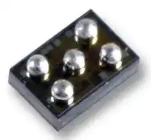
## CSPEMI204 ## EMI Filter with ESD Protection ## **Product Description** The CSPEMI204 is an L−R−C EMI filter array with ESD protection that integrates two Pi−filters (C−L−R−C) to suppress EMI/RFI Noise. CSPEMI204 includes ESD protection diodes on all input/output pins, and provides a very high level of protection for sensitive electronic components against possible electrostatic discharge (ESD). The ESD diodes connected to the filter ports safely dissipate ESD strikes of 30 kV, which is beyond the maximum requirement of the IEC61000−4−2 international standard. ## **www.onsemi.com** **WLCSP5** IEC61000−4−2 international standard. **FC SUFFIX CASE 567MA Features** Two Channels of EMI Filtering 30 kV ESD Protection (IEC 61000−4−2, Contact Discharge) **BLOCK DIAGRAM** 1®) 30 kV ESD Protection (IEC 61000−4−2, Air Discharge) ~~Oe~~ Filter#1 Filter#2 Greater than 45 dB of Attenuation at 900 MHz A1 C1 A3 C3 These Devices are Pb−Free, Halogen Free/BFR Free and are RoHS 4 ~~, oy~~ Compliant **Applications** GND B1 GND B1 Mobile Phones AE ~~GAN~~ **MAXIMUM RATINGS** (TA = 25C) **MARKING DIAGRAM** ~~O ~~~~ **Rating Symbol Value Unit** ATM ~~INA~~ ESD Discharge IEC61000−4−2Contact Discharge " Vpp 30 ~~gO~~ kV AT = Specific Device Code oy Air Discharge 30 M = Date Code ~~ANEw”~~ RMS Current per Line ILine 350 mA Operating Temperature Range TJ −40 to +125 C **ORDERING INFORMATION** ~~Poek~~ Storage Temperature Range ~~© \IWee OMITeo~~ Tstg −55 to +150 C **Device Package Shipping**[[†]] Lead Solder Temperature TL 260 C CSPEMI204FCTAG WLCSP5 5000 / Tape & (10 second duration) (Pb−Free) Reel ~~eT] tJFeFe~~ ## **Features** - Two Channels of EMI Filtering - 30 kV ESD Protection (IEC 61000−4−2, Contact Discharge) - 30 kV ESD Protection (IEC 61000−4−2, Air Discharge) - Greater than 45 dB of Attenuation at 900 MHz - These Devices are Pb−Free, Halogen Free/BFR Free and are RoHS Compliant ## **Applications** - Mobile Phones **ORDERING INFORMATION Device Package Shipping**[[†]] CSPEMI204FCTAG WLCSP5 5000 / Tape & (Pb−Free) Reel ~~tJFeFe~~ †For information on tape and reel specifications, including part orientation and tape sizes, please refer to our Tape and Reel Packaging Specification Brochure, BRD8011/D. Stresses exceeding those listed in the Maximum Ratings table may damage the device. If any of these limits are exceeded, device functionality should not be assumed, damage may occur and reliability may be affected. Publication Order Number: **1** Semiconductor Components Industries, LLC, 2015 **August, 2024 − Rev. 1** **CSPEMI204/D** **CSPEMI204** ## **Table 1. PIN DESCRIPTIONS** |**Pin**|**Name**|**Description**| |---|---|---| |A1|Filter #1|Filter #1 Input/Output| |C1|Filter #1|Filter #1 Input/Output| |A3|Filter #2|Filter #2 Input/Output| |C3|Filter #2|Filter #2 Input/Output| |B2|GND|Device Ground| ## **PACKAGE/PINOUT DIAGRAMS** **==> picture [213 x 113] intentionally omitted <==** **----- Start of picture text -----**<br> Top View Bottom View<br>(Bumps Down View) (Bumps Up View)<br>Orientation<br>C B A Marking<br>+<br>1 A1 C1<br>AT 2 B2<br>A3 C3<br>3<br>WLCSP5 Package<br>+<br>**----- End of picture text -----**<br> **Table 2. ELECTRICAL OPERATING CHARACTERISTICS** (TA = 25C unless otherwise noted) |**Symbol**|**Parameter**|**Test Conditions**|**Min**|**Typ**|**Max**|**Unit**| |---|---|---|---|---|---|---| |VRWM|Working Voltage|||3.0||V| |VBR|Breakdown Voltage|IT= 1 mA; (Note 4)|6.0|||V| |ILEAK|Channel Leakage Current|VIN= 3.0 V,GND = 0 V|||400|nA| |RCH|Channel Resistance<br>(Pins A1 – A3, C1 – C3)||||3.0|�| |Ct|Line Capacitance|VR= 0 V, f = 1 MHz|185|250|315|pF| |f3dB|Cutoff Frequency|450� Source and<br>10 k�Load Termination||2.0||MHz| |f3dB|Cutoff Frequency|50�Termination||25||MHz| |Fatten|Stop Band Attenuation|@ 700 MHz<br>@ 900 MHz||40<br>47||dB| |VESD|Insystem ESD Withstand Voltage<br>a) Contact discharge per IEC 6100042 standard, Level 4<br>**(External Pins)**<br>b) Contact discharge per IEC 6100042 standard, Level 1<br>**(Internal Pins)**|(Notes 1 and 2)|30<br>30|||kV| |VCL|TLP Clamping Voltage|Forward IPP= 8 A<br>Forward IPP= 16 A<br>Forward IPP=8 A<br>Forward IPP=16 A||9.8<br>11.5<br>−9.7<br>−11.7||V| Product parametric performance is indicated in the Electrical Characteristics for the listed test conditions, unless otherwise noted. Product performance may not be indicated by the Electrical Characteristics if operated under different conditions. 1. Standard IEC61000−4−2 with CDischarge = 150 pF , RDischarge = 330, GND grounded. 2. These measurements performed with no external capacitor . 3. TVS devices are normally selected according to the working peak reverse voltage (VRWM), which should be equal to or greater than the DC or continuous peak operating voltage level. 4. VBR is measured at pulse test current IT. **www.onsemi.com** **2** **CSPEMI204** ## **PERFORMANCE INFORMATION** ## **Typical Filter Performance** **==> picture [493 x 407] intentionally omitted <==** **----- Start of picture text -----**<br> 0 0<br>−10<br>−10<br>−20<br>−30<br>−20<br>−40<br>−30 −50<br>−60<br>−40<br>−70<br>−80<br>−50<br>−90<br>−60 −100<br>1.E+05 1.E+06 1.E+07 1.E+08 1.E+09 1.E+10 1.E+05 1.E+06 1.E+07 1.E+08 1.E+09 1.E+10 1.E+11<br>FREQUENCY (Hz) FREQUENCY (Hz)<br>Figure 1. Typical Insertion Loss (50 � Figure 3. Typical Insertion Loss (450 � Source<br>Termination) and 10 k � Load Termination)<br>−80<br>−85<br>−90<br>−95<br>−100<br>−105<br>−110<br>−115<br>−120<br>20 200 2000 20000<br>FREQUENCY (Hz)<br>Figure 2. Typical THD+N at 1.8 Vpp<br>S21 (dB) S21 (dB)<br>THD+N (dB)<br>**----- End of picture text -----**<br> **www.onsemi.com** **3** **CSPEMI204** **IEC 61000−4−2 Spec.** |**Level**|**Test Volt-**<br>**age (kV)**|**First Peak**<br>**Current**<br>**(A)**|**Current at**<br>**30 ns (A)**|**Current at**<br>**60 ns (A)**| |---|---|---|---|---| |1|2|7.5|4|2| |2|4|15|8|4| |3|6|22.5|12|6| |4|8|30|16|8| **==> picture [231 x 156] intentionally omitted <==** **----- Start of picture text -----**<br> IEC61000−4−2 Waveform<br>Ipeak<br>100%<br>90%<br>I @ 30 ns<br>I @ 60 ns<br>10%<br>tP = 0.7 ns to 1 ns<br>**----- End of picture text -----**<br> **Figure 4. IEC61000−4−2 Spec** **==> picture [441 x 120] intentionally omitted <==** **----- Start of picture text -----**<br> ESD Gun Oscilloscope<br>TVS<br>50 �<br>Cable 50 �<br>**----- End of picture text -----**<br> **Figure 5. Diagram of ESD Clamping Voltage Test Setup** **The following is taken from Application Note AND8308/D − Interpretation of Datasheet Parameters for ESD Devices.** ## **ESD Voltage Clamping** For sensitive circuit elements it is important to limit the voltage that an IC will be exposed to during an ESD event to as low a voltage as possible. The ESD clamping voltage is the voltage drop across the ESD protection diode during an ESD event per the IEC61000−4−2 waveform. Since the IEC61000−4−2 was written as a pass/fail spec for larger systems such as cell phones or laptop computers it is not clearly defined in the spec how to specify a clamping voltage at the device level. ON Semiconductor has developed a way to examine the entire voltage waveform across the ESD protection diode over the time domain of an ESD pulse in the form of an oscilloscope screenshot, which can be found on the datasheets for all ESD protection diodes. For more information on how ON Semiconductor creates these screenshots and how to interpret them please refer to AND8307/D. **www.onsemi.com** **4** **CSPEMI204** **==> picture [491 x 438] intentionally omitted <==** **----- Start of picture text -----**<br> 25 −25<br>20 −20<br>Pty ete e y EEE<br>15 ee −15 eeeT Ey<br>10 Pitt −10 a<br>tT ety) LEE<br>5 −5<br>|i tig | ) LT LL ee<br>0 0<br>TIT ¥YIiT) LEEtd¥i<br>0 2 4 6 8 10 12 14 0 −2 −4 −6 −8 −10 −12 −14<br>VC, VOLTAGE (V) VC, VOLTAGE (V)<br>Figure 6. Positive TLP I−V Curve (Preliminary) Figure 7. Negative TLP I−V Curve (Preliminary)<br>NOTE: TLP parameter: Z0 = 50 : tp = 100 ns, tr = 300 ps, averaging window: t1 = 30 ns to t2 = 60 ns. VIEC is the equivalent voltage N<br>stress level calculated at the secondary peak of the IEC 61000−4−2 waveform at t = 30 ns with 2 A/kV. See TLP description<br>\O<br>below for more information.<br>Transmission Line Pulse (TLP) Measurement Transmission Line Pulse (TLP) provides current versus L e a S Attenuator l 50 CoaxCable<br>voltage (I−V) curves in which each data point is obtained <br>from a 100 ns long rectangular pulse from a charged 50 Coax<br>transmission line. A simplified schematic of a typical TLP Cable 10 M IM VM<br>system is shown in Figure 8. TLP I−V curves of ESD<br>protection devices accurately demonstrate the product’s<br>DUT<br>ESD capability because the 10s of amps current levels and AN O% V R C O L.<br>under 100 ns time scale match those of an ESD event. This w We, SE O T oyL<br>Oscilloscope<br>is illustrated in Figure 9 where an 8 kV IEC 61000−4−2<br>O WE Qe = :<br>current waveform is compared with TLP current pulses at<br>Figure 8. Simplified Schematic of a Typical TLP<br>8 A and 16 A. A TLP I−V curve shows the voltage at which G ar oF System<br>the device turns on as well as how well the device clamps<br>voltage over a range of current levels. ONO<br>Qc<br>TLP CURRENT (A) TLP CURRENT (A)<br>**----- End of picture text -----**<br> ## **Transmission Line Pulse (TLP) Measurement** **Figure 9. Comparison Between 8 kV IEC 61000−4−2 and 8 A and 16 A TLP Waveforms** **www.onsemi.com** **5** # MECHANICAL CASE OUTLINE **PACKAGE DIMENSIONS** # **SCALE 4:1** # **WLCSP5, 1.26x0.89** CASE 567MA ISSUE O # DATE 07 JUL 2015 **==> picture [436 x 282] intentionally omitted <==** **----- Start of picture text -----**<br> E A B NOTES:1. DIMENSIONING AND TOLERANCING PER ASME<br>REFERENCEPIN A1 Y14.5M, 1994.<br>2. CONTROLLING DIMENSION: MILLIMETERS.<br>ÈÈ 3. COPLANARITY APPLIES TO SPHERICAL<br>CROWNS OF SOLDER BALLS.<br>ÈÈ D 4. DIMENSION b IS MEASURED AT THE MAXIMUM<br>BALL DIAMETER PARALLEL TO DATUM C.<br>2X 0.10 C MILLIMETERS<br>DIM MIN MAX<br>A −−− 0.50<br>2X 0.10 C TOP VIEW A1 0.18 0.22<br>A2 0.255 REF<br>b 0.235 0.295<br>A2 D 1.26 BSC<br>E 0.89 BSC<br>0.10 C e 0.50 BSC<br>e1 0.435 BSC<br>A<br>GENERIC<br>0.05 C<br>SEATING MARKING DIAGRAM*<br>NOTE 3 A1 SIDE VIEW C PLANE<br>XXM<br>e/2<br>XX = Specific Device Code<br>5X b e M = Date Code<br>0.10 C A B e1<br>C *This information is generic. Please refer to<br>0.05 C device data sheet for actual part marking.<br>B Pb−Free indicator, “G” or microdot “ � ”,<br>may or may not be present.<br>A<br>1 2 3 RECOMMENDED<br>SOLDERING FOOTPRINT*<br>BOTTOM VIEW<br>**----- End of picture text -----**<br> **==> picture [146 x 105] intentionally omitted <==** **----- Start of picture text -----**<br> PACKAGE<br>A1 OUTLINE<br>5X 0.27<br>0.87<br>PITCH<br>0.50<br>PITCH<br>DIMENSIONS: MILLIMETERS<br>**----- End of picture text -----**<br> # *For additional information on our Pb−Free strategy and soldering details, please download the ON Semiconductor Soldering and Mounting Techniques Reference Manual, SOLDERRM/D. Electronic versions are uncontrolled except when accessed directly from the Document Repository. **DOCUMENT NUMBER: 98AON00069G** Printed versions are uncontrolled except when stamped “CONTROLLED COPY” in red. **DESCRIPTION: WLCSP5, 1.26X0.89 PAGE 1 OF 1** # **onsemi** and are trademarks of Semiconductor Components Industries, LLC dba **onsemi** or its subsidiaries in the United States and/or other countries. **onsemi** reserves the right to make changes without further notice to any products herein. **onsemi** makes no warranty, representation or guarantee regarding the suitability of its products for any particular purpose, nor does **onsemi** assume any liability arising out of the application or use of any product or circuit, and specifically disclaims any and all liability, including without limitation special, consequential or incidental damages. **onsemi** does not convey any license under its patent rights nor the rights of others. # Semiconductor Components Industries, LLC, 2015 # www.onsemi.com **onsemi** , , and other names, marks, and brands are registered and/or common law trademarks of Semiconductor Components Industries, LLC dba “ **onsemi** ” or its affiliates and/or subsidiaries in the United States and/or other countries. **onsemi** owns the rights to a number of patents, trademarks, copyrights, trade secrets, and other intellectual property. A listing of **onsemi** ’s product/patent coverage may be accessed at www.onsemi.com/site/pdf/Patent−Marking.pdf. **onsemi** reserves the right to make changes at any time to any products or information herein, without notice. The information herein is provided “as−is” and **onsemi** makes no warranty, representation or guarantee regarding the accuracy of the information, product features, availability, functionality, or suitability of its products for any particular purpose, nor does **onsemi** assume any liability arising out of the application or use of any product or circuit, and specifically disclaims any and all liability, including without limitation special, consequential or incidental damages. Buyer is responsible for its products and applications using **onsemi** products, including compliance with all laws, regulations and safety requirements or standards, regardless of any support or applications information provided by **onsemi** . “Typical” parameters which may be provided in **onsemi** data sheets and/or specifications can and do vary in different applications and actual performance may vary over time. All operating parameters, including “Typicals” must be validated for each customer application by customer’s technical experts. **onsemi** does not convey any license under any of its intellectual property rights nor the rights of others. **onsemi** products are not designed, intended, or authorized for use as a critical component in life support systems or any FDA Class 3 medical devices or medical devices with a same or similar classification in a foreign jurisdiction or any devices intended for implantation in the human body. Should Buyer purchase or use **onsemi** products for any such unintended or unauthorized application, Buyer shall indemnify and hold **onsemi** and its officers, employees, subsidiaries, affiliates, and distributors harmless against all claims, costs, damages, and expenses, and reasonable attorney fees arising out of, directly or indirectly, any claim of personal injury or death associated with such unintended or unauthorized use, even if such claim alleges that **onsemi** was negligent regarding the design or manufacture of the part. **onsemi** is an Equal Opportunity/Affirmative Action Employer. This literature is subject to all applicable copyright laws and is not for resale in any manner. ## **ADDITIONAL INFORMATION** **TECHNICAL PUBLICATIONS** : **ONLINE SUPPORT** : www.onsemi.com/support **Technical Library:** www.onsemi.com/design/resources/technical−documentation **For additional information, please contact your local Sales Representative at onsemi Website:** www.onsemi.com www.onsemi.com/support/sales **==> picture [232 x 43] intentionally omitted <==**
Updated at April 28, 2026
onsemi is a premier global supplier of intelligent power and sensing technologies, driving disruptive innovations across the automotive, industrial, and cloud infrastructure markets. Recognized for their commitment to sustainability and reliable supply chains, the company accelerates advancements in vehicle electrification, industrial automation, and 5G networks by solving the industry's most complex design challenges. At the core of their portfolio is an industry-leading selection of discrete semiconductors. This extensive range features thousands of high-performance bipolar transistors, single and dual MOSFETs, and a comprehensive array of diodes, including Zener, Schottky, and fast-recovery rectifiers. Engineered for superior thermal performance and energy efficiency, these foundational components are critical for demanding power conversion, switching, and signal conditioning applications. Beyond essential discretes, onsemi provides a robust suite of advanced power management and circuit protection solutions. Their lineup includes intelligent power modules, single IGBTs, and transient voltage suppression (TVS) diodes designed to safeguard sensitive circuitry. Complimented by integrated passive filters, AC/DC LED driver ICs, and specialized sub-2.4GHz RF transceivers, onsemi equips engineers with the scalable, high-quality technologies needed to build a cleaner, smarter, and more connected world.
About Novapart
Novapart is a B2B electronic component broker specialising in stock shortages and cost reduction. We source hard-to-find parts and identify compliant alternatives across a catalogue of 410,000+ components from 500+ manufacturers.
Learn more →Stock Shortage Specialist
When a component is unavailable, discontinued or has an unacceptable lead time, we tap into our network of vetted European and Asian distributors to source what you need — without compromising on quality or traceability.
Request a quote →Compliant Alternatives
We identify pin-to-pin, electrically equivalent substitutes that meet the same certifications (RoHS, AEC-Q100, REACH) as your original specification — validated against datasheets, not just part numbers. Often at a lower cost.
BOM Analysis service →