
Image not available
Illustrative purposes only

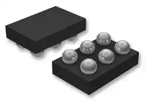
CSD75301W1015
Dual MOSFET, P Channel, 20 V, 1.2 A
⚠️ Reference pricing provided. In case of supply shortages, we will connect you with our trusted procurement partners to ensure your project's continuity.
- Manufacturer: TEXAS INSTRUMENTS
- Product type: Dual MOSFETs
- Transistor Polarity:Dual P Channel; Continuous Drain Current Id:-1.2A; Drain Source Voltage Vds:-20V; On Resistance Rds(on):0.08ohm; Rds(on) Test Vo; Available until stocks are exhausted
- MSL: MSL 1 - Unlimited
- No. of Pins: 6Pins
- Channel Type: P Channel
- Product Range: -
- Qualification: -
- Transistor Case Style: DSBGA
- Operating Temperature Max: 150°C
- Power Dissipation N Channel: -
- Power Dissipation P Channel: 800mW
- Drain Source Voltage Vds N Channel: -
- Drain Source Voltage Vds P Channel: 20V
- Continuous Drain Current Id N Channel: -
- Continuous Drain Current Id P Channel: 1.2A
- Drain Source On State Resistance N Channel: -
- Drain Source On State Resistance P Channel: 0.08ohm
| Delivery and price | |
|---|---|
| Units per pack | 500 |
| Price | 0.292 € |
| Current stock | 500+ |
| Lead time | 30 days |
Datasheet

**CSD75301W1015**

SLPS212C –AUGUST 2009–REVISED MARCH 2012

**www.ti.com**

## **P-Channel NexFET™Power MOSFET**

**Check for Samples: CSD75301W1015**

## **1FEATURES**

- **Dual P-Ch MOSFETs**

- **Common Source Configuration**

- **Small Footprint 1mm × 1.5mm**

- **Low Profile – 0.62mm**

- **Ultra Low Qg and Qgd**

- **Pb Free / RoHS Compliant**

- **Halogen Free**

## **APPLICATIONS**

- **Battery Management**

- **Load Switch**

- **Battery Protection**

## **DESCRIPTION**

The device has been designed to deliver the lowest on resistance and gate charge in the smallest outline possible with excellent thermal characteristics in an ultra low profile.

**Figure 1. Top View**

**==> picture [66 x 87] intentionally omitted <==**

**----- Start of picture text -----**<br>
D2 G2<br>S S<br>G1 D1<br>O<br>**----- End of picture text -----**<br>


## **PRODUCT SUMMARY**

|**PRODUCT SUMMARY**|**PRODUCT SUMMARY**|**PRODUCT SUMMARY**|**PRODUCT SUMMARY**|**PRODUCT SUMMARY**|
|---|---|---|---|---|
|(Per MOSFET unless otherwise stated)|||||
|VDS|Drain to Source Voltage|–20||V|
|Qg|Gate Charge Total (4.5V)|1.5||nC|
|Qgd|Gate Charge Gate to Drain|0.3||nC|
|RDS(on)|Drain to Source On Resistance|VGS = –1.8V|150|mΩ|
|||VGS= –2.5V|105|mΩ|
|||VGS= –4.5V|80|mΩ|
|VGS(th)|Voltage threshold|–0.7||V|


VGS(th)

|**ORDERING INFORMATION**||
|---|---|
|**Device**<br>**Package**<br>**Media**<br>**Qty**<br>1 × 1.5 Wafer<br>CSD75301W1015<br>7-inch reel<br>3000<br>Level Package<br>~~eeee~~|**Ship**<br>Tape and<br>Reel|


## **ABSOLUTE MAXIMUM RATINGS**

|TA= 25°C unless otherwise stated|TA= 25°C unless otherwise stated|**VALUE**|**UNIT**|
|---|---|---|---|
|VDS|Drain to Source Voltage|–20|V|
|VGS|Gate to Source Voltage|±8|V|
|ID|Continuous Drain Current, TC= 25°C(1) (2)|–1.2|A|
|IDM|Pulsed Drain Current, TA= 25°C(1) (2) (3)|–17.5|A|
|PD|Power Dissipation(1) (2)|0.8|W|
|TJ,<br>TSTG|Operating Junction and Storage<br>Temperature Range|–55 to 150|°C|


- (1) Per device, both devices in conduction.

- (2) R θ JA = 74°C/W on 1in[2] Cu (2 oz.) on 0.060" thick FR4 PCB.

- (3) Pulse width ≤ 300 μ s, duty cycle ≤ 2%

**RDS(ON) vs VGS**

## **Gate Charge**

**==> picture [431 x 123] intentionally omitted <==**

**----- Start of picture text -----**<br>
300 6<br>ID = −1A ID = −1A<br>250 5 V DS  = −10V<br>200 T J  = 125°C 4<br>150 pf 3 ieer ae<br>100 a cane 2 74am<br>50 SSS TJ = 25°C 1<br>0 0<br>0 SEE 1 2 3 4 5 6 0.00 Y 0.25 i titty 0.50 0.75 1.00 1.25 1.50 1.75 | 2.00<br>−VGS − Gate to Source Voltage − V G006 Qg − Gate Charge − nC G003<br>Ω<br> − Gate Voltage − V<br>G<br> − On-State Resistance − m −V<br>DS(on)<br>R<br>**----- End of picture text -----**<br>


Please be aware that an important notice concerning availability, standard warranty, and use in critical applications of Texas Instruments semiconductor products and disclaimers thereto appears at the end of this data sheet. ~~Be~~

PRODUCTION DATA information is current as of publication date. Products conform to specifications per the terms of the Texas Instruments standard warranty. Production processing does not necessarily include testing of all parameters.

Copyright © 2009–2012, Texas Instruments Incorporated

**CSD75301W1015**

SLPS212C –AUGUST 2009–REVISED MARCH 2012

**www.ti.com**

## **ELECTRICAL CHARACTERISTICS**

(TA = 25°C unless otherwise stated) (Per MOSFET unless otherwise stated)

|**PARAMETER**|**PARAMETER**|**TEST CONDITIONS**|**MIN**<br>**TYP**<br>**MAX**|**UNIT**|
|---|---|---|---|---|
|**Static Characteristics**|||||
|BVDSS|Drain to Source Voltage|VGS = 0V, ID = –250μA|–20|V|
|IDSS|Drain to Source Leakage Current|VGS = 0V, VDS = –16V|–1|μA|
|IGSS|Gate to Source Leakage Current|VDS = 0V, VGS = –8V|–100|nA|
|VGS(th)|Gate to Source Threshold Voltage|VDS = VGS, ID = –250μA|–0.4<br>–0.7<br>–1.0|V|
|RDS(on)|Drain to Source On Resistance|VGS = –1.8V, ID = –1A|150<br>190|mΩ|
|||VGS = –2.5V, ID = –1A|105<br>135|mΩ|
|||VGS = –4.5V, ID = –1A|80<br>100|mΩ|
|gfs|Transconductance|VDS = –10V, ID = –1A|5.2|S|
|**Dynamic**|**Characteristics**||||
|CISS|Input Capacitance|VGS= 0V, VDS= –10V, f = 1MHz|150<br>195|pF|
|COSS|Output Capacitance||67<br>87|pF|
|CRSS|Reverse Transfer Capacitance||24<br>31|pF|
|Qg|Gate Charge Total(–4.5V)|VDS= –10V, ID= –1A|1.5<br>2.1|nC|
|Qgd|Gate Charge Gate to Drain||0.3|nC|
|Qgs|Gate Charge Gate to Source||0.28|nC|
|Qg(th)|Gate Charge at Vth||0.12|nC|
|QOSS|Output Charge|VDS = –9.5V, VGS = 0V|1.1|nC|
|td(on)|Turn On Delay Time|VDS= –10V, VGS= –4.5V, ID= –1A<br>RG= 30Ω|3|ns|
|tr|Rise Time||1.7|ns|
|td(off)|Turn Off Delay Time||38|ns|
|tf|Fall Time||16|ns|
|**Diode Characteristics**|||||
|VSD|Diode Forward Voltage|IS = –1A, VGS = 0V|–0.81<br>–1|V|
|Qrr|Reverse RecoveryCharge|Vdd = –9.5V, IF = –1A, di/dt = 200A/μs|2|nC|
|trr|Reverse RecoveryTime|Vdd = –9.5V, IF = –1A, di/dt = 200A/μs|7.5|ns|


## **THERMAL CHARACTERISTICS**

(TA = 25°C unless otherwise stated)

|**THERMAL CHARACTERISTICS**<br>(TA = 25°C unless otherwise stated)|||
|---|---|---|
|**PARAMETER**|**MIN**<br>**TYP**<br>**MAX**|**UNIT**|
|R θJC<br>Thermal Resistance Junction to Ambient(1) (2)|136|°C/W|
|R θJA<br>Thermal Resistance Junction to Ambient(2) (3)|93|°C/W|


(1) Device mounted on FR4 material with Minimum Cu mounting area.

(2) Measured with both devices biased in a parallel condition.

(3) Device mounted on FR4 material with 1in[2] of 2 oz Cu.

2

Copyright © 2009–2012, Texas Instruments Incorporated

**CSD75301W1015**

SLPS212C –AUGUST 2009–REVISED MARCH 2012

**www.ti.com**

**==> picture [122 x 13] intentionally omitted <==**

**----- Start of picture text -----**<br>
P - Chan 1.0x1.5 CSP TTA MAX Rev1<br>**----- End of picture text -----**<br>


**==> picture [88 x 106] intentionally omitted <==**

**==> picture [110 x 85] intentionally omitted <==**

**----- Start of picture text -----**<br>
Max R θ JA = 93°C/W<br>when mounted on<br>1inch [2] of 2 oz. Cu.<br>M0155-01<br>**----- End of picture text -----**<br>


**==> picture [122 x 13] intentionally omitted <==**

**----- Start of picture text -----**<br>
P - Chan 1.0x1.5 CSP TTA MIN Rev1<br>**----- End of picture text -----**<br>


**==> picture [45 x 74] intentionally omitted <==**

**==> picture [17 x 3] intentionally omitted <==**

**----- Start of picture text -----**<br>
M0156-01<br>**----- End of picture text -----**<br>


**==> picture [104 x 45] intentionally omitted <==**

**----- Start of picture text -----**<br>
Max R θ JA = 136°C/W<br>when mounted on<br>minimum pad area of 2<br>oz. Cu.<br>**----- End of picture text -----**<br>


## **TYPICAL MOSFET CHARACTERISTICS**

**==> picture [496 x 234] intentionally omitted <==**

**----- Start of picture text -----**<br>
(TA = 25°C unless otherwise stated)<br>10<br>1<br>0.5<br>0.3<br>0.1 0.1<br>0.05 Duty Cycle = t1/t2<br>0.02<br>0.01 0.01 P<br>t1<br>Single Pulse t2<br>0.001 R�JA = 109�C/W (min Cu)<br>T J = P � Z �JA � R �JA<br>0.0001<br>0.00001 0.0001 0.001 0.01 0.1 1 10 100 1k<br>t – Pulse Duration – s<br>p<br>G012<br>– Normalized Thermal Impedance<br>JA<br>�<br>Z<br>**----- End of picture text -----**<br>


**Figure 2. Transient Thermal Impedance**

3

Copyright © 2009–2012, Texas Instruments Incorporated

**CSD75301W1015**

SLPS212C –AUGUST 2009–REVISED MARCH 2012

**www.ti.com**

## **TYPICAL MOSFET CHARACTERISTICS (continued)**

(TA = 25°C unless otherwise stated)

**==> picture [225 x 572] intentionally omitted <==**

**----- Start of picture text -----**<br>
5.0<br>4.5<br>4.0 VGS = −4.5V<br>3.5<br>VGS = −3V VGS = −1.5V<br>3.0<br>2.5 VGS = −2.5V<br>2.0<br>1.5<br>1.0 VGS = −2V<br>0.5<br>0.0<br>0.0 0.5 1.0 1.5 2.0 2.5 3.0<br>−VDS − Drain to Source Voltage − V G001<br>Figure 3. Saturation Characteristics<br>6<br>ID = −1A<br>5 V DS  = −10V<br>4<br>3<br>2<br>1<br>0<br>0.00 0.25 0.50 0.75 1.00 1.25 1.50 1.75 2.00<br>Qg − Gate Charge − nC G003<br>Figure 5. Gate Charge<br>1.0<br>0.9 I D  = −250µA<br>0.8<br>0.7<br>0.6<br>0.5<br>0.4<br>0.3<br>0.2<br>0.1<br>0.0<br>−75 −25 25 75 125 175<br>TJ − Junction Temperature − °C G005<br> − Drain Current − A<br>D<br>−I<br> − Gate Voltage − V<br>G<br>−V<br> − Threshold Voltage − V<br>GS(th)<br>−V<br>**----- End of picture text -----**<br>


**Figure 7. Threshold Voltage vs. Temperature**

**==> picture [224 x 572] intentionally omitted <==**

**----- Start of picture text -----**<br>
5<br>VDS = −5V<br>4<br>3<br>TJ = 125°C<br>2<br>TJ = 25°C<br>1<br>TJ = −55°C<br>0<br>0.50 0.75 1.00 1.25 1.50 1.75 2.00 2.25 2.50<br>−VGS − Gate to Source Voltage − V G002<br>Figure 4. Transfer Characteristics<br>200<br>180 f = 1MHz<br>VGS = 0V<br>160<br>140<br>120 COSS = CDS + CGD<br>CISS = CGD + CGS<br>100<br>80<br>60 C RSS  = C GD<br>40<br>20<br>0<br>0 5 10 15 20<br>−VDS − Drain to Source Voltage − V G004<br>Figure 6. Capacitance<br>300<br>ID = −1A<br>250<br>200 T J  = 125°C<br>150<br>100<br>50 TJ = 25°C<br>0<br>0 1 2 3 4 5 6<br>−VGS − Gate to Source Voltage − V G006<br> − Drain Current − A<br>D<br>−I<br>C − Capacitance − pF<br>Ω<br> − On-State Resistance − m<br>DS(on)<br>R<br>**----- End of picture text -----**<br>


**Figure 8. On Resistance vs. Gate Voltage**

4

Copyright © 2009–2012, Texas Instruments Incorporated

**CSD75301W1015**

SLPS212C –AUGUST 2009–REVISED MARCH 2012

**www.ti.com**

## **TYPICAL MOSFET CHARACTERISTICS (continued)**

(TA = 25°C unless otherwise stated)

**==> picture [225 x 362] intentionally omitted <==**

**----- Start of picture text -----**<br>
1.6<br>ID = −1A<br>1.4<br>V GS  = −4.5V<br>1.2<br>1.0<br>0.8<br>0.6<br>0.4<br>0.2<br>0.0<br>−75 −25 25 75 125 175<br>TJ − Case Temperature − °C G007<br>Figure 9. On Resistance vs. Temperature<br>100<br>10<br>1ms<br>1<br>10ms<br>Area�Limited 100ms<br>0.1<br>by�RDS(on) 1s<br>DC<br>Single�Pulse<br>R θJA =�109�C/W�(min�Cu)<br>0.01<br>0.1 1 10 100<br>−VDS −Drain To�Source�Voltage −V G009<br> −Drain�Current −A<br>D<br>−I<br>Normalized On-State Resistance<br>**----- End of picture text -----**<br>


**Figure 11. Maximum Safe Operating Area**

**==> picture [225 x 361] intentionally omitted <==**

**----- Start of picture text -----**<br>
10<br>1 TJ = 125°C<br>0.1<br>TJ = 25°C<br>0.01<br>0.001<br>0.0001<br>0.0 0.2 0.4 0.6 0.8 1.0 1.2<br>−VSD − Source to Drain Voltage − V G008<br>Figure 10. Typical Diode Forward Voltage<br>1.4<br>1.2<br>1.0<br>0.8<br>0.6<br>0.4<br>0.2<br>0.0<br>−50 −25 0 25 50 75 100 125 150 175<br>TJ − Junction Temperature − °C G011<br> − Source to Drain Current − A<br>SD<br>−I<br> − Drain Current − A<br>D<br>−I<br>**----- End of picture text -----**<br>


**Figure 12. Maximum Drain Current vs. Temperature**

5

Copyright © 2009–2012, Texas Instruments Incorporated

**CSD75301W1015**

SLPS212C –AUGUST 2009–REVISED MARCH 2012

**www.ti.com**

## **MECHANICAL DATA**

## **CSD75301W1015 Package Dimensions**

**==> picture [475 x 379] intentionally omitted <==**

**----- Start of picture text -----**<br>
Pin 1 Solder Ball Pin 1<br>Mark Ø 0.31 ±0.075 Mark<br>1 2 2 1<br>A A<br>B B<br>C C<br>1.00 [+0.00] –0.10 0.62 Max 0.50<br>Top View Side View Bottom View<br>Seating Plate<br>Front View<br>–0.10<br>0.50<br>+0.00<br>1.00<br>1.50<br>0.38<br>0.04<br>0.62 Max<br>**----- End of picture text -----**<br>


M0157-01

NOTE: All dimensions are in mm (unless othersse specified)

## **Pinout**

|**POSITION**|**DESIGNATION**|
|---|---|
|B1, B2|Source|
|C1|Gate1|
|C2|Drain1|
|A2|Gate2|
|A1|Drain2|


6

Copyright © 2009–2012, Texas Instruments Incorporated

**CSD75301W1015**

SLPS212C –AUGUST 2009–REVISED MARCH 2012

**www.ti.com**

## **Land Pattern Recommendation**

**==> picture [494 x 523] intentionally omitted <==**

**----- Start of picture text -----**<br>
Ø 0.25<br>1 2<br>A<br>B<br>C<br>0.50<br>M0158-01<br>NOTE: All dimensions are in mm (unless othersse specified)<br>Tape and Reel Information<br>4.00�±0.10 2.00�±0.05 Ø�1.50�±0.10<br>2°�Max<br>4.00�±0.10 Ø 0.60 [+0.05] –0.10<br>0.86�±0.05 0.254�±0.02<br>2°�Max<br>1.19�±0.05<br>M0159-01<br>0.50<br>1.00<br>+0.30 –0.10<br>8.00 1.75�±0.10<br>3.50�±0.05<br>1.65�±0.05<br>**----- End of picture text -----**<br>


## **Tape and Reel Information**

NOTE: All dimensions are in mm (unless othersse specified)

7

Copyright © 2009–2012, Texas Instruments Incorporated

**CSD75301W1015**

SLPS212C –AUGUST 2009–REVISED MARCH 2012

**www.ti.com**

## **REVISION HISTORY**

|**Changes from Original (August 2009) to Revision A**<br>**Page**|
|---|
|•<br>Changed location of the Pin 1 indicator dot in the pin out illustration. .................................................................................. 1|
|**Changes from Revision A (November 2009) to Revision B**<br>**Page**|
|•<br>Deleted the Package Marking Information section ............................................................................................................... 7|
|**Changes from Revision B (November 2009) to Revision C**<br>**Page**|
|•<br>Changed the CSD75301W1015 Package Dimensions section. Top View From: 15.00 To: 1.50 ........................................ 6|


8

Copyright © 2009–2012, Texas Instruments Incorporated

## **IMPORTANT NOTICE**

Texas Instruments Incorporated and its subsidiaries (TI) reserve the right to make corrections, modifications, enhancements, improvements, and other changes to its products and services at any time and to discontinue any product or service without notice. Customers should obtain the latest relevant information before placing orders and should verify that such information is current and complete. All products are sold subject to TI ’ s terms and conditions of sale supplied at the time of order acknowledgment.

TI warrants performance of its hardware products to the specifications applicable at the time of sale in accordance with TI ’ s standard warranty. Testing and other quality control techniques are used to the extent TI deems necessary to support this warranty. Except where mandated by government requirements, testing of all parameters of each product is not necessarily performed.

TI assumes no liability for applications assistance or customer product design. Customers are responsible for their products and applications using TI components. To minimize the risks associated with customer products and applications, customers should provide adequate design and operating safeguards.

TI does not warrant or represent that any license, either express or implied, is granted under any TI patent right, copyright, mask work right, or other TI intellectual property right relating to any combination, machine, or process in which TI products or services are used. Information published by TI regarding third-party products or services does not constitute a license from TI to use such products or services or a warranty or endorsement thereof. Use of such information may require a license from a third party under the patents or other intellectual property of the third party, or a license from TI under the patents or other intellectual property of TI.

Reproduction of TI information in TI data books or data sheets is permissible only if reproduction is without alteration and is accompanied by all associated warranties, conditions, limitations, and notices. Reproduction of this information with alteration is an unfair and deceptive business practice. TI is not responsible or liable for such altered documentation. Information of third parties may be subject to additional restrictions.

Resale of TI products or services with statements different from or beyond the parameters stated by TI for that product or service voids all express and any implied warranties for the associated TI product or service and is an unfair and deceptive business practice. TI is not responsible or liable for any such statements.

TI products are not authorized for use in safety-critical applications (such as life support) where a failure of the TI product would reasonably be expected to cause severe personal injury or death, unless officers of the parties have executed an agreement specifically governing such use. Buyers represent that they have all necessary expertise in the safety and regulatory ramifications of their applications, and acknowledge and agree that they are solely responsible for all legal, regulatory and safety-related requirements concerning their products and any use of TI products in such safety-critical applications, notwithstanding any applications-related information or support that may be provided by TI. Further, Buyers must fully indemnify TI and its representatives against any damages arising out of the use of TI products in such safety-critical applications.

TI products are neither designed nor intended for use in military/aerospace applications or environments unless the TI products are specifically designated by TI as military-grade or " enhanced plastic. " Only products designated by TI as military-grade meet military specifications. Buyers acknowledge and agree that any such use of TI products which TI has not designated as military-grade is solely at the Buyer ' s risk, and that they are solely responsible for compliance with all legal and regulatory requirements in connection with such use.

TI products are neither designed nor intended for use in automotive applications or environments unless the specific TI products are designated by TI as compliant with ISO/TS 16949 requirements. Buyers acknowledge and agree that, if they use any non-designated products in automotive applications, TI will not be responsible for any failure to meet such requirements.

Following are URLs where you can obtain information on other Texas Instruments products and application solutions:

|**Products**<br>Audio<br>Amplifiers<br>Data Converters<br>DLP® Products<br>DSP<br>Clocks and Timers<br>Interface<br>Logic<br>Power Mgmt<br>Microcontrollers<br>RFID<br>OMAP Mobile Processors<br>Wireless Connectivity|**Applications**<br>www.ti.com/audio<br>Automotive and Transportation <br>amplifier.ti.com<br>Communications and Telecom<br>dataconverter.ti.com<br>Computers and Peripherals<br>www.dlp.com<br>Consumer Electronics<br>dsp.ti.com<br>Energy and Lighting<br>www.ti.com/clocks<br>Industrial<br>interface.ti.com<br>Medical<br>logic.ti.com<br>Security<br>power.ti.com<br>Space, Avionics and Defense<br>microcontroller.ti.com<br>Video and Imaging<br>www.ti-rfid.com<br>www.ti.com/omap<br>www.ti.com/wirelessconnectivity<br>**TI E2E Community Home Page**|www.ti.com/automotive<br>www.ti.com/communications<br>www.ti.com/computers<br>www.ti.com/consumer-apps<br>www.ti.com/energy<br>www.ti.com/industrial<br>www.ti.com/medical<br>www.ti.com/security<br>www.ti.com/space-avionics-defense|
|---|---|---|
|||www.ti.com/video<br>e2e.ti.com|


Mailing Address: Texas Instruments, Post Office Box 655303, Dallas, Texas 75265 Copyright © 2012, Texas Instruments Incorporated
Updated at June 9, 2026
About Novapart
Novapart is a B2B electronic component broker specialising in stock shortages and cost reduction. We source hard-to-find parts and identify compliant alternatives across a catalogue of 410,000+ components from 500+ manufacturers.
Learn more →Stock Shortage Specialist
When a component is unavailable, discontinued or has an unacceptable lead time, we tap into our network of vetted European and Asian distributors to source what you need — without compromising on quality or traceability.
Request a quote →Compliant Alternatives
We identify pin-to-pin, electrically equivalent substitutes that meet the same certifications (RoHS, AEC-Q100, REACH) as your original specification — validated against datasheets, not just part numbers. Often at a lower cost.
BOM Analysis service →