
Image not available
Illustrative purposes only

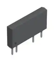
CPC1926Y
MOSFET RELAY, SPST-NO, 0.7A, 250V, THT
⚠️ Reference pricing provided. In case of supply shortages, we will connect you with our trusted procurement partners to ensure your project's continuity.
- Manufacturer: IXYS SEMICONDUCTOR
- Product type: MOSFET Solid State Relays
- Load Type: AC / DC
- Contact Form: SPST-NO (1 Form A)
- Load Current: 700mA
- Product Range: OptoMOS Series
- Relay Mounting: Through Hole
- Relay Terminals: PC Pin
- Load Voltage Max: 250V
- Isolation Voltage: 2.5kV
- I/O Capacitance Typ: 2pF
- On State Resistance Max: 1.4ohm
- MOSFET Relay Package Style: SIP-8 (4-Pin Used)
- Off State Leakage Current Max: 1µA
| Delivery and price | |
|---|---|
| Units per pack | 500 |
| Price | 3.31 € |
| Current stock | 10+ |
| Lead time | 30 days |
Datasheet

**CPC1926 Single-Pole, Normally Open OptoMOS[®] Power SIP Relay**
INTEGRATED CIRCUITS DIVISION
|**Parameter**|**Rating**|**Units**|
|---|---|---|
|Blocking Voltage|250|VP|
|Load Current|0.7|Arms/ ADC|
|On-Resistance(max)|1.4||
## **Description**
IXYS Integrated Circuits brings OptoMOS[®] technology, reliability, and compact size to a new family of high-power, solid state relays. As part of that family, the CPC1926 is a single-pole, normally open (1-Form-A) solid state relay.
## **Features**
- Handle Load Currents Up to 0.7 ADC/Arms
- 2500Vrms Input/Output Isolation
- Power SIP Package
- High Reliability
- No Moving Parts
- Low Drive Power Requirements
- Arc-Free With No Snubbing Circuits
- No EMI/RFI Generation
The CPC1926 employs optically coupled MOSFET technology to provide 2500Vrms of input to output isolation. The optically coupled outputs, that use patented OptoMOS architecture, are controlled by a highly efficient infrared LED. The combination of low on-resistance and high load-current handling capabilities makes the relay suitable for a variety of high-performance switching applications.
- Flammability Rating UL 94 V-0
## **Approvals**
## **Applications**
- UL 508 Certified Component: File E69938
- Industrial Controls
- Motor Control
- Robotics
- Medical Equipment—Patient/Equipment Isolation
- Instrumentation
- Multiplexers
- Data Acquisition
- Electronic Switching
- I/O Subsystems
- Meters (Watt-Hour, Water, Gas)
- IC Equipment
- Home Appliances
## **Ordering Information**
**==> picture [238 x 151] intentionally omitted <==**
**----- Start of picture text -----**<br>
Part # Description<br>—EE CPC1926Y 4-Pin (8-Pin Body) Power SIP Package (25 per tube)<br>Pin Configuration<br>1 2 3 4<br>- +<br>**----- End of picture text -----**<br>
## **Pin Configuration**
**Switching Characteristics of Normally Open Devices**
**==> picture [158 x 102] intentionally omitted <==**
**----- Start of picture text -----**<br>
Form-A<br>I<br>F<br>90%<br>10%<br>I<br>LOAD<br>t t<br>on off<br>**----- End of picture text -----**<br>
**1**
DS-CPC1926-R07
**www.ixysic.com**
**CPC1926**
INTEGRATED CIRCUITS DIVISION
## **Absolute Maximum Ratings @ 25ºC**
|**Parameter**|**Ratings**|**Units**|
|---|---|---|
|BlockingVoltage|250|VP|
|Reverse Input Voltage|5|V|
|Input control Current<br>Peak(10ms)|50|mA|
||1|A|
|Input Power Dissipation1|150|mW|
|Total Power Dissipation2|2400|mW|
|Isolation voltage Input to Output|2500|Vrms|
|Operational Temperature|-40 to +85|°C|
|Storage Temperature|-40 to +125|°C|
_Absolute Maximum Ratings are stress ratings. Stresses in excess of these ratings can cause permanent damage to the device. Functional operation of the device at conditions beyond those indicated in the operational sections of this data sheet is not implied._
_Typical values are characteristic of the device at +25°C, and are the result of engineering evaluations. They are provided for information purposes only, and are not part of the manufacturing testing requirements._
1 Derate linearly 1.33 mW / ºC
2 Derate linearly 20 mW / ºC
## **Electrical Characteristics @ 25ºC**
|**Parameter**|**Conditions**|**Symbol**|**Min**|**Typ**|**Max**|**Units**|
|---|---|---|---|---|---|---|
|**Output Characteristics**|||||||
|Load Current, Continuous|Free air|IL|-|-|0.7|Arms/ ADC|
|Peak Load Current|t<10ms|ILPK|-|-|±3|AP|
|On-Resistance1|IL=100mA|RON|-|1.2|1.4||
|Off-State Leakage Current|VL=250VP|ILEAK|-|-|1|µA|
|Switching Speeds<br>Turn-On<br>Turn-Off|||||||
||IF=10mA, VL=10V|ton|-|2.3|10|ms|
|||toff|-|0.022|10||
|Output Capacitance|IF=0mA, VL=50V, f=1MHz|COUT|-|60|-|pF|
|**Input Characteristics**|||||||
|Input Control Current to Activate|IL=120mA|IF|-|3.75|10|mA|
|Input Control Current to Deactivate|-|IF|0.6|-|-|mA|
|Input Voltage Drop|IF=10mA|VF|0.9|1.35|1.56|V|
|Reverse Input Current|VR=5V|IR|-|-|10|µA|
|**Input/Output Characteristics**|||||||
|Capacitance Input/Output|VIO=0V, f=1MHz|CIO|-|2|-|pF|
1 Measurement taken within 1 second of on-time.
**Thermal Characteristics**
**Parameter Conditions Symbol Min Typ Max Units** ~~SS~~ Thermal Impedance (junction to case) - R JC - 1.5 - °C/W
R07
**www.ixysic.com**
**2**
all INTEGRATED CIRCUITS DIVISION **CPC1926** ~~De~~ EEE)
## **PERFORMANCE DATA***
**==> picture [498 x 572] intentionally omitted <==**
**----- Start of picture text -----**<br>
Typical LED Forward Voltage Drop Typical Turn-On Time Typical Turn-Off Time<br>(N=50, IF=10mA, TA=25ºC) (N=50, IF=10mA, IL=5mADC, TA=25ºC) (N=50, IF=10mA, IL=5mADC, TA=25ºC)<br>35 25 25<br>30<br>20 20 FL | | Td<br>25<br>20 15 15 Te<br>15 10 10 r | | | hu<br>10<br>5 5 Se<br>5<br>0 0 0 i i il i = i i<br>1.260 1.265 1.270 1.275 1.280 1.8 2.0 2.2 2.4 2.6 2.8 0.015 0.017 0.019 0.021 0.023 0.025<br>LED Forward Voltage (V) Turn-On Time (ms) Turn-Off Time (ms)<br>Typical On-Resistance Distribution Typical Blocking Voltage Distribution<br>(N=50, IF=10mA, IL=0.7ADC, TA=25ºC) (N=50, TA=25ºC)<br>35 35<br>30 ee 30 Fe] fT tT tl<br>25 me Pe 25 Ft ft hE hE hE<br>20 me! Pe 20 Ft | tT ht hE<br>15 me! Pe 15 a<br>10 me! Ee 10 | ee<br>5 ee 5 | ho<br>0 a ill lll=z 0 rSli) | | 6 ==<br>1.17 1.19 1.21 1.23 1.25 1.27 265 267 269 271 273 275 277<br>On-Resistance ( ) Blocking Voltage (VP)<br>Typical Turn-On Time Typical Turn-Off Time<br>Typical LED Forward Voltage Drop vs.LED Forward Current vs. LED Forward Current<br>vs. Temperature (IL=100mADC) (IL=100mADC)<br>1.8 5.0 0.09<br>4.5 0.08<br>1.6 4.0 0.07<br>SSOP 3.5 REESE 0.06 GS<br>1.4 3.0<br>IF=50mA 2.5 0.05<br>1.2 IF=20mA 2.0 0.04<br>PRSSSor= IF=10mA 6 1.5 AREERPEREECEEETT TS 0.03 | CESply tt tt tT tt<br>1.0 1.0 0.02<br>0.5 0.01<br>0.8 F LEET LE 0 EERE EEE 0 DEREE E E E<br>-40 -20 0 20 40 60 80 100 120 0 5 10 15 20 25 30 35 40 45 50 0 5 10 15 20 25 30 35 40 45 50<br>Temperature (ºC) LED Forward Current (mA) LED Forward Current (mA)<br>Typical IF for Switch Operation<br>vs. Temperature Typical Turn-On Time vs. Temperature Typical Turn-Off Time vs. Temperature<br>(IL=100mADC) (IL=100mADC) (IL=100mADC)<br>5.50 1.4 0.07<br>5.25 pot ft ff tt 1.2 fF | | ht hE IF=10mA 0.06 EF otT ThE hE rT<br>5.00<br>4.75 oe 1.0 ee ee a 0.05 PELELLEL,<br>4.50 po 0.8 {ft tr | 0.04 | IF=20mA<br>4.25<br>4.003.75 eeeEe 0.60.4 a ae IF=20mA 0.030.02 2Ef | |Tl rT| | IF=10mA<br>3.50<br>3.25 0.2 0.01<br>3.00 ee ee 0 e e ee ee ee 0 ree<br>-40 -20 0 20 40 60 80 100 -40 -20 0 20 40 60 80 100 -40 -20 0 20 40 60 80 100<br>Temperature (ºC) Temperature (ºC) Temperature (ºC)<br>Device Count (N) Device Count (N) Device Count (N)<br>Device Count (N) Device Count (N)<br>Turn-On Time (ms) Turn-Off Time (ms)<br>LED Forward Voltage Drop (V)<br>LED Current (mA) Turn-On Time (ms) Turn-Off Time (ms)<br>**----- End of picture text -----**<br>
*Unless otherwise noted, data presented in these graphs is typical of device operation at 25ºC. For guaranteed parameters not indicated in the written specifications, please contact our application department.
**www.ixysic.com**
R07
**3**
**CPC1926**
INTEGRATED CIRCUITS DIVISION
## a
## **PERFORMANCE DATA***
**==> picture [529 x 284] intentionally omitted <==**
**----- Start of picture text -----**<br>
Typical On-Resistance<br>vs. Temperature Typical Load Current vs. Load Voltage Maximum Load Current<br>(IF=10mA, IL=100mADC) (IF=10mA, TA=25ºC) vs. Temperature<br>3.5 1.25 1.4<br>3.0 2ee 1.000.75 ee 1.2 eee<br>o 2.5 F [| | [| [ | [ | 0.50 es 1.0 r | | | | [tt<br>2.0 Feo | | hE dT 0.25 ee 0.8 r | {| | | | ft<br>0.00<br>1.5 Fe fT UE hE—-hdT hee -0.25 -—_____}___1_ 0.6 es ee ee ee ee<br>1.0 72m 4 -0.50 Ee | | 7, | | 0.4 —}—}—_ SS<br>0.5 — -0.75 0.2<br>cs [O] ae [n] -1.00 ee a ee rf | | eRe<br>0 7 -1.25 BEFLL]a {| [| | [| 0.0 F e tT ETT TEE<br>-40 -20 0 20 40 60 80 100 -1.5 -1.0 -0.5 0 0.5 1.0 1.5 -40 -20 0 20 40 60 80 100 120<br>Temperature (ºC) Load Voltage (V) Temperature (ºC)<br>Typical Leakage vs. Temperature<br>Measured across Pins 3 & 4 Energy Rating Curve<br>Blocking Voltage vs. Temperature (VL=250V) Free Air, No Heat Sink<br>300 0.035 4.0<br>295 Ss es 0.030 Ft ft fff dtd 3.5 LILO<br>290 ee 0.025 FTP 3.0 28011 01 AN AH<br>285280 2aee 0.020 ae 2.52.0 2010000 SU<br>0.015 TSE 20100000<br>275 Ft 1.5 0<br>0.010<br>270 F | ott _ Tet 1.0 200 0 SU<br>265 F | Atotft ttt 0.005 potats] | 0.5 0)3010001)00/ 0 0 a00<br>260 re ee 0 F teteLEL LL 0.0 a mu 00001) 0000<br>-40 -20 0 20 40 60 80 100 -40 -20 0 20 40 60 80 100 10 Mw s 100 Mw s 1ms 10ms 100ms 1s 10s 100s<br>Temperature (ºC) Temperature (ºC) Time<br>IF=20mA<br>IF=10mA<br>)<br>) rms<br>/A<br>DC<br>On-Resistance ( Load Current (A)<br>Load Current (A<br>)P<br>A)<br>Leakage (<br>Blocking Voltage (V Load Current (A)<br>**----- End of picture text -----**<br>
*Unless otherwise noted, data presented in these graphs is typical of device operation at 25ºC. For guaranteed parameters not indicated in the written specifications, please contact our application department.
R07
**www.ixysic.com**
**4**
**CPC1926**
INTEGRATED CIRCUITS DIVISION
## **Manufacturing Information**
## **Moisture Sensitivity**
All plastic encapsulated semiconductor packages are susceptible to moisture ingression. IXYS Integrated Circuits classifies its plastic encapsulated devices for moisture sensitivity according to the latest version of % the joint industry standard, **IPC/JEDEC J-STD-020** , in force at the time of product evaluation. We test all of our products to the maximum conditions set forth in the standard, and guarantee proper operation of our devices when handled according to the limitations and information in that standard as well as to any limitations set forth in the information or standards referenced below.
Failure to adhere to the warnings or limitations as established by the listed specifications could result in reduced product performance, reduction of operable life, and/or reduction of overall reliability.
This product carries a Moisture Sensitivity Level (MSL) classification as shown below, and should be handled according to the requirements of the latest version of the joint industry standard **IPC/JEDEC J-STD-033** .
|**Device**<br>~~pT~~|**Moisture Sensitivity Level (MSL) Classifi cation**<br>~~pT~~|
|---|---|
|CPC1926Y<br>~~pT~~|MSL 1<br>~~pT~~|
## **ESD Sensitivity**
This product is **ESD Sensitive** , and should be handled according to the industry standard **JESD-625** .
## **Soldering Profile**
Provided in the table below is the Classification Temperature (TC) of this product and the maximum dwell time the body temperature of this device may be (TC - 5)ºC or greater. The classification temperature sets the Maximum Body Temperature allowed for this device during lead-free reflow processes. For through-hole devices, and any other processes, the guidelines of **J-STD-020** must be observed.
**Device Classifi cation Temperature (Tc) Dwell Time (tp) Max Refl ow Cycles** CPC1926Y 245ºC 30 seconds 1 ~~SSee~~ **Board Wash** IXYS Integrated Circuits recommends the use of no-clean flux formulations. Board washing to reduce or remove flux residue following the solder reflow process is acceptable provided proper precautions are taken to prevent damage to the device. These precautions include, but are not limited to: using a low pressure wash and providing a follow up bake cycle sufficient to remove any moisture trapped within the device due to the washing process. Due to the variability of the wash parameters used to clean the board, determination of the bake temperature and duration necessary to remove the moisture trapped within the package is the responsibility of the user (assembler). Cleaning or drying methods that employ ultrasonic energy may damage the device and should not be used. Additionally, the device must not be exposed to flux or solvents that are Chlorine- or Fluorine-based.
**www.ixysic.com**
R07
**5**
**CPC1926**
INTEGRATED CIRCUITS DIVISION
## **MECHANICAL DIMENSIONS**
## **CPC1926Y**
**==> picture [486 x 223] intentionally omitted <==**
**----- Start of picture text -----**<br>
(0.830±0.015)21.082±0.381 3.302±0.051 PCB Hole Pattern<br>(0.130±0.002)<br>1.150 DIA. x4<br>1.75 (0.045 DIA. x4)<br>(0.069)<br>10.160±0.127<br>(0.400±0.005) 7º TYP<br>4 Places<br>5.080<br>(0.200)<br>Pin 1<br>1.016±0.127 10.160<br>Pin 1<br>(0.040±0.005) (0.400)<br>1.778<br>4.572±0.127<br>(0.070) 2.540<br>(0.180±0.005)<br>0.381±0.013 (0.100)<br>0.762±0.076 10.160±0.127 (0.015±0.0005)<br>(0.030±0.003) (0.400±0.005) 1.651±0.102<br>2.540±0.12 7 5.080±0.127 (0.065±0.004) 1.778<br>(0.100±0.005) rie (0.200±0.005) (0.070) yt<br>7º TYP<br>4 Places<br>Note: Pin-to-pin tolerances are non-cumulative.<br>Dimensions<br>mm<br>__7 - (inches)<br>**----- End of picture text -----**<br>
## **For additional information please visit our website at: www.ixysic.com**
IXYS Integrated Circuits makes no representations or warranties with respect to the accuracy or completeness of the contents of this publication and reserves the right to make changes to specifications and product descriptions at any time without notice. Neither circuit patent licenses nor indemnity are expressed or implied. Except as set forth in IXYS Integrated Circuits' Standard Terms and Conditions of Sale, IXYS Integrated Circuits assumes no liability whatsoever, and disclaims any express or implied warranty, relating to its products including, but not limited to, the implied warranty of merchantability, fitness for a particular purpose, or infringement of any intellectual property right.
The products described in this document are not designed, intended, authorized or warranted for use as components in systems intended for surgical implant into the body, or in other applications intended to support or sustain life, or where malfunction of IXYS Integrated Circuits' product may result in direct physical harm, injury, or death to a person or severe property or environmental damage. IXYS Integrated Circuits reserves the right to discontinue or make changes to its products at any time without notice.
Specification: DS-CPC1926-R07 ©Copyright 2018, IXYS Integrated Circuits OptoMOS[®] is a registered trademark of IXYS Integrated Circuits All rights reserved. Printed in USA. 6/20/2018
**6**
Updated at February 9, 2023
About Novapart
Novapart is a B2B electronic component broker specialising in stock shortages and cost reduction. We source hard-to-find parts and identify compliant alternatives across a catalogue of 410,000+ components from 500+ manufacturers.
Learn more →Stock Shortage Specialist
When a component is unavailable, discontinued or has an unacceptable lead time, we tap into our network of vetted European and Asian distributors to source what you need — without compromising on quality or traceability.
Request a quote →Compliant Alternatives
We identify pin-to-pin, electrically equivalent substitutes that meet the same certifications (RoHS, AEC-Q100, REACH) as your original specification — validated against datasheets, not just part numbers. Often at a lower cost.
BOM Analysis service →