
Image not available
Illustrative purposes only

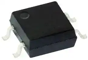
CPC1025N
MOSFET RELAY, SPST-NO, 0.12A, 400V, SMD
⚠️ Reference pricing provided. In case of supply shortages, we will connect you with our trusted procurement partners to ensure your project's continuity.
- Manufacturer: IXYS SEMICONDUCTOR
- Product type: MOSFET Solid State Relays
- Contact Form:SPST-NO (1 Form A); Load Type:AC / DC; Load Voltage Max:400V; Load Current:120mA; MOSFET Relay Package Style:SOP-4; Relay Mounting:Surface Mount; 03M7311
- SVHC: No SVHC (25-Jun-2025)
- Load Type: AC / DC
- Contact Form: SPST-NO (1 Form A)
- Load Current: 120mA
- Product Range: OptoMOS Series
- Relay Mounting: Surface Mount
- Relay Terminals: Gull Wing
- Load Voltage Max: 400V
- Isolation Voltage: 1.5kV
- I/O Capacitance Typ: 1pF
- On State Resistance Max: 30ohm
- MOSFET Relay Package Style: SOP-4
- Off State Leakage Current Max: 1µA
| Delivery and price | |
|---|---|
| Units per pack | 5000 |
| Price | 0.913 € |
| Current stock | 500+ |
| Lead time | 30 days |
Datasheet

**CPC1025N 400V Normally-Open Single-Pole 4-Pin SOP OptoMOS[®] Relay**
INTEGRATED CIRCUITS DIVISION
|**Parameter**|**Rating**|**Units**|
|---|---|---|
|BlockingVoltage|400|VP|
|Load Current|120|mArms/ mADC|
|On-Resistance(max)|30||
## **Features**
- 1500Vrms Input/Output Isolation
- Small 4-Pin SOP Package
## **Description**
The CPC1025N is a miniature normally-open (1-Form-A) solid state relay in a 4-pin SOP package that employs optically coupled MOSFET technology to provide 1500Vrms of input to output isolation. The efficient MOSFET switches and photovoltaic die use IXYS Integrated Circuits Division’s patented OptoMOS architecture while the optically coupled output is controlled by a highly efficient infrared LED.
- Low Drive Power Requirements
- High Reliability
- Arc-Free With No Snubbing Circuits
- No EMI/RFI Generation
- Tape & Reel Version Available
- Flammability Rating UL 94 V-0
## **Applications**
- Telecommunications
- Telecom Switching
- Tip/Ring Circuits
- Modem Switching (Laptop, Notebook, Pocket Size)
- Hook Switch
The CPC1025N uses IXYS Integrated Circuits Division’s state of the art double-molded vertical construction packaging to produce one of the world’s smallest relays. It offers board space savings of at least 20% over the competitor’s larger 4-pin SOP relay.
## **Approvals**
- UL Recognized Component: File E76270
- CSA Certified Component: Certificate 1172007
- EN/IEC 60950-1 Certified Component: TUV Certificate B 13 12 82667 003
- Dial Pulsing
- Ground Start
- Ringing Injection
- Instrumentation
- Multiplexers
- Data Acquisition
- Electronic Switching
- I/O Subsystems
- Meters (Watt-Hour, Water, Gas)
- Medical Equipment—Patient/Equipment Isolation
- Security
- Aerospace
- Industrial Controls
**Ordering Information**
**==> picture [238 x 131] intentionally omitted <==**
**----- Start of picture text -----**<br>
Part # Description<br>CPC1025N 4-Pin SOP (100/tube)<br>—— CPC1025NTR 4-Pin SOP (2000/reel)<br>Pin Configuration<br>1 4<br>+ Control Load<br>2 3<br>– Control Load<br>**----- End of picture text -----**<br>
## **Pin Configuration**
**Switching Characteristics of Normally-Open Devices**
**==> picture [98 x 64] intentionally omitted <==**
**----- Start of picture text -----**<br>
Form-A<br>IF<br>90%<br>10%<br>ILOAD<br>ton toff<br>**----- End of picture text -----**<br>
**1**
DS-CPC1025N-R09
**www.ixysic.com**
**CPC1025N**
INTEGRATED CIRCUITS DIVISION
## **Absolute Maximum Ratings @ 25ºC**
|**Parameter**|**Ratings**|**Units**|
|---|---|---|
|BlockingVoltage|400|VP|
|Reverse Input Voltage|5|V|
|Input Control Current<br>Peak (10ms)|50|mA|
||1|A|
|Input Power Dissipation1|70|mW|
|Total Power Dissipation2|400|mW|
|Capacitance, Input to Output|1|pF|
|Isolation Voltage, Input to Output|1500|Vrms|
|Operational Temperature|-40 to +85|°C|
|Storage Temperature|-40 to +125|°C|
_Absolute Maximum Ratings are stress ratings. Stresses in excess of these ratings can cause permanent damage to the device. Functional operation of the device at conditions beyond those indicated in the operational sections of this data sheet is not implied._
_Typical values are characteristic of the device at +25°C, and are the result of engineering evaluations. They are provided for information purposes only, and are not part of the manufacturing testing requirements._
1 Derate linearly 1.33 mW / ºC
2 Derate linearly 3.33 mW / ºC
## **Electrical Characteristics @ 25ºC**
|**Parameter**|**Conditions**|**Symbol**|**Min**|**Typ**|**Max**|**Units**|
|---|---|---|---|---|---|---|
|**Output Characteristics**<br>~~ee~~|||||||
|Load Current<br>Continuous1<br>Peak<br>~~ee~~|-<br>~~ee~~|IL<br>~~ee~~|-<br>~~ee~~|-<br>~~ee~~|120<br>~~ee~~|mArms/ mADC<br>~~ee~~|
||t=10ms<br>~~ee~~|ILPK<br>~~ee~~|-<br>~~ee~~|-<br>~~ee~~|±350<br>~~ee~~|mAP<br>~~ee~~|
|On-Resistance2<br>~~ee~~|IF=5mA, IL=120mA<br>~~ee~~|RON<br>~~ee~~|-<br>~~ee~~|25<br>~~ee~~|30<br>~~ee~~|<br>~~ee~~|
|Off-State Leakage Current<br>~~ee~~|VL=400VP<br>~~ee~~|ILEAK<br>~~ee~~|-<br>~~ee~~|-<br>~~ee~~|1<br>~~ee~~|µA<br>~~ee~~|
|Switching Speeds<br>Turn-On<br>Turn-Off<br>~~ee~~|IF=5mA, VL=10V<br>~~ee~~|ton<br>~~ee~~|-<br>~~ee~~|-<br>~~ee~~|2<br>~~ee~~|ms<br>~~ee~~|
|||toff<br>~~ee~~|-<br>~~ee~~|-<br>~~ee~~|1<br>~~ee~~||
|Output Capacitance|IF=0mA, VL=50V, f=1MHz|COUT|-|77|-|pF|
|**Input Characteristics**|||||||
|Input Control Current to Activate3|IL=120mA|IF|-|0.8|2|mA|
|Input Control Current to Deactivate|-|IF|0.3|0.6|-|mA|
|Input Voltage Drop|IF=5mA|VF|0.9|1.2|1.5|V|
|Reverse Input Current|VR=5V|IR|-|-|10|µA|
1 Load current derates linearly from 120mA @ 25oC to 80mA @ 85oC.
2 Measurement taken within 1 second of on-time.
3 For applications requiring high temperature operation (greater than 60°C) a minimum LED drive current of 4mA is recomended.
R09
**www.ixysic.com**
**2**
**CPC1025N**
INTEGRATED CIRCUITS DIVISION
## **PERFORMANCE DATA***
**==> picture [315 x 127] intentionally omitted <==**
**----- Start of picture text -----**<br>
Typical LED Forward Voltage Drop Typical Turn-On Time<br>(N=50, IF=5mA) (N=50, IF=5mA, IL=120mA)<br>35 25<br>30<br>20 Ft dE dT TT [|<br>25<br>20 15 FLlt<br>15 10 7a) | ee|<br>10<br>5 7a | ee<br>50 0 | Eee<br>1.17 1.19 1.21 1.23 1.25 0.50 0.60 0.70 0.80 0.90 1.00 1.10<br>LED Forward Voltage Drop (V) Turn-On Time (ms)<br>Device Count (N) Device Count (N)<br>**----- End of picture text -----**<br>
**==> picture [147 x 126] intentionally omitted <==**
**----- Start of picture text -----**<br>
Typical Turn-Off Time<br>(N=50, IF=5mA, IL=120mA)<br>25<br>20<br>15<br>10<br>5<br>0<br>0.21 0.22 0.23 0.24 0.25 0.26 0.27<br>Turn-Off Time (ms)<br>Device Count (N)<br>**----- End of picture text -----**<br>
**==> picture [487 x 275] intentionally omitted <==**
**----- Start of picture text -----**<br>
Typical IF for Switch Operation Typical IF for Switch Dropout Typical On-Resistance Distribution<br>(N=50, IL=120mA) (N=50, IL=120mA) (N=50, IF=2mA, IL=120mA)<br>25 25 35<br>30<br>20 Ft dE dT TT [| 20 FE | cE dT TL pf | | ft ft<br>25<br>15 SOEeeee) 15 occ = 20<br>10 t+ | Bi | 10 73 |Gee 15 EEPTT<br>10<br>5 =—|\ 5 fe TT<br>5<br>0 | Bee Ge e 0 s| Bae|| oo 0 s/t|=<br>0.45 0.50 0.55 0.60 0.65 0.70 0.75 0.45 0.50 0.55 0.60 0.65 0.70 0.75 23.5 24 24.5 25 25.5 26 26.5<br>LED Current (mA) LED Current (mA) On-Resistance ( )<br>Typical Blocking Voltage Distribution<br>(N=50)<br>35<br>30252015105 777|mma hdl 2eehdl<br>0 [ | Enna |<br>420 425 430 435 440 445 450<br>Blocking Voltage (VP)<br>Device Count (N) Device Count (N) Device Count (N)<br>Device Count (N)<br>**----- End of picture text -----**<br>
**==> picture [492 x 137] intentionally omitted <==**
**----- Start of picture text -----**<br>
Typical Turn-On Time Typical Turn-Off Time<br>Typical LED Forward Voltage Drop vs. LED Forward Current vs. LED Forward Current<br>vs. Temperature (IL=120mA) (IL=120mA)<br>1.8 2.0 1.4<br>1.8<br>1.2<br>1.6 <SRReeee 1.6 REE EEE FL ET te tt yt<br>1.4 1.0<br>1.4 SPER 1.2 ose 0.8 A<br>1.0<br>1.2 0.8 0.6<br>0.6 0.4<br>1.0 SSS 0.4 ARSE PETE Py<br>PELE SERRE, 0.2 EEE<br>0.2<br>0.8 P LE LLL EI 0 OO 0 7<br>-40 -20 0 20 40 60 80 100 120 0 5 10 15 20 25 30 35 40 45 50 0 5 10 15 20 25 30 35 40 45 50<br>Temperature (ºC) LED Forward Current (mA) LED Forward Current (mA)<br>IIIIIFFFFF=50mA=30mA=20mA=10mA=5mA Turn-On Time (ms) Turn-Off Time (ms)<br>LED Forward Voltage Drop (V)<br>**----- End of picture text -----**<br>
*Unless otherwise noted, data presented in these graphs is typical of device operation at 25ºC. For guaranteed parameters not indicated in the written specifications, please contact our application department.
**www.ixysic.com**
R09
**3**
anil INTEGRATED CIRCUITS DIVISION **CPC1025N** ~~De~~ EEE)
## **PERFORMANCE DATA***
**==> picture [495 x 423] intentionally omitted <==**
**----- Start of picture text -----**<br>
Typical Turn-On Time vs. Temperature Typical Turn-Off Time vs. Temperature Typical On-Resistance vs. Temperature<br>(IL=80mA) (IL=80mA) (IF=10mA, IL=80mA)<br>2.0 1.0 60<br>0.9<br>Se a 50 FT...<br>0.8<br>1.5<br>IF=5mA 0.70.6 SEEERES = 40 CEP<br>1.0 0.5 30<br>IF=10mA 0.40.3 SEESPSs 20 EERE_+—_|<br>0.5 0.2 IF=10mA 10<br>0.1 Sse EPS<br>0 0 oe ee ee IF=5mA 0 FELEE Tt<br>-40 -20 0 20 40 60 80 100 -40 -20 0 20 40 60 80 100 -40 -20 0 20 40 60 80 100<br>Temperature (ºC) Temperature (ºC) Temperature (ºC)<br>Typical IF for Switch Operation Typical IF for Switch Dropout<br>vs. Temperature vs. Temperature Typical Load Current vs. Load Voltage<br>(IL=80mA) (IL=80mA) (IF=5mA)<br>3.0 3.0 150<br>2.5 FL | tT cE TT 2.5 FLT oT dT hE TT 100<br>2.0 2.0 50<br>FL | tT cE LT pt | tT tt<br>1.5 1.5 0<br>FT oT | | pt tT |TTA<br>1.0 1.0 -50<br>|] eet pot ft | per<br>0.5 poet | 0.5 pop et -100<br>0 FEE EE 0 FLT E E -150<br>-40 -20 0 20 40 60 80 100 -40 -20 0 20 40 60 80 100 -3 -2 -1 0 1 2 3<br>Temperature (ºC) Temperature (ºC) Load Voltage (V)<br>Typical Leakage vs. Temperature<br>Typical Blocking Voltage Measured Across Pins 3&4<br>Maximum Load Current vs. Temperature vs. Temperature (VL=400V)<br>180 455 0.016<br>160 FtTEftEtTfttll 450 ee 0.014 Fel. [ |]<br>140120 arf {| { [ [ | ft 445 Fett of IL4 0.0120.010 ra | | |f[tfdid | [| { |<br>100 0 440<br>80 F 435 0.008<br>ee ee See Foto [et fT 0.006 es<br>60<br>40 epfe{ | f PNT F 430 wae 0.004 ae=<br>20 es 425 Lx 0.002 rf | ]<br>0 Foe Lr 420 e et et tT tt 0 E+ Tt. | [ttt]<br>-40 -20 0 20 40 60 80 100 120 -40 -20 0 20 40 60 80 100 -40 -20 0 20 40 60 80 100<br>Temperature (ºC) Temperature (ºC) Temperature (ºC)<br>I =5mA<br>I =2mA<br>Turn-On Time (ms) Turn-Off Time (ms) On-Resistance ()<br>LED Current (mA) LED Current (mA) Load Current (mA)<br>)P<br>Leakage (µA)<br>Load Current (mA) Blocking Voltage (V<br>**----- End of picture text -----**<br>
**==> picture [329 x 125] intentionally omitted <==**
**----- Start of picture text -----**<br>
Output Capacitance vs. Load Voltage<br>700 (IF=0mA, f=1MHz) 1.0 Energy Rating Curve<br>0.9<br>600 rT tstffsttl 00000000<br>0.8<br>500 Clery 0.7 30000<br>400 ret 0.6 0<br>0.5<br>300 Cm 0.4 A)2000 0 0 00 0<br>200 A | | | | | 0.3 S00123010000880000 0<br>0.2<br>100 A 0.1 000 S00<br>0 EL tt 0 a230000 00 0 000<br>0 50 100 150 200 250 300 10 s 100 s 1ms 10ms 100ms 1s 10s 100s<br>Load Voltage (V) Time<br>Load Current (A)<br>Output Capacitence (pF)<br>**----- End of picture text -----**<br>
*Unless otherwise noted, data presented in these graphs is typical of device operation at 25ºC. For guaranteed parameters not indicated in the written specifications, please contact our application department.
R09
**www.ixysic.com**
**4**
**CPC1025N**
INTEGRATED CIRCUITS DIVISION
## **Manufacturing Information**
## **Moisture Sensitivity**
All plastic encapsulated semiconductor packages are susceptible to moisture ingression. IXYS Integrated Circuits Division classifies its plastic encapsulated devices for moisture sensitivity according to the latest ¢) version of the joint industry standard, **IPC/JEDEC J-STD-020** , in force at the time of product evaluation. We test all of our products to the maximum conditions set forth in the standard, and guarantee proper operation of our devices when handled according to the limitations and information in that standard as well as to any limitations set forth in the information or standards referenced below.
Failure to adhere to the warnings or limitations as established by the listed specifications could result in reduced product performance, reduction of operable life, and/or reduction of overall reliability.
This product carries a Moisture Sensitivity Level (MSL) classification as shown below, and should be handled according to the requirements of the latest version of the joint industry standard **IPC/JEDEC J-STD-033** .
|**Device**<br>~~—~~|**Moisture Sensitivity Level (MSL) Classifi cation**<br>~~eee~~|
|---|---|
|CPC1025N<br>~~—~~|MSL 3<br>~~eee~~|
## **ESD Sensitivity**
This product is **ESD Sensitive** , and should be handled according to the industry standard **JESD-625** .
## **Soldering Profile**
Provided in the table below is the Classification Temperature (TC) of this product and the maximum dwell time the body temperature of this device may be (TC - 5)ºC or greater. The classification temperature sets the Maximum Body Temperature allowed for this device during lead-free reflow processes. For through-hole devices, and any other processes, the guidelines of **J-STD-020** must be observed.
|**Device**<br>**Classifi cation Temperature (Tc)**<br>**Dwell Time (tp)**<br>**Max Refl ow Cycles**<br>CPC1025N<br>260ºC<br>30 seconds<br>3<br>~~————————E~~|
|---|
|**Board Wash**|
IXYS Integrated Circuits Division recommends the use of no-clean flux formulations. Board washing to reduce or remove flux residue following the solder reflow process is acceptable provided proper precautions are taken to prevent damage to the device. These precautions include, but are not limited to: using a low pressure wash and providing a follow up bake cycle sufficient to remove any moisture trapped within the device due to the washing process. Due to the variability of the wash parameters used to clean the board, determination of the bake temperature and duration necessary to remove the moisture trapped within the package is the responsibility of the user (assembler). Cleaning or drying methods that employ ultrasonic energy may damage the device and should not be used. Additionally, the device must not be exposed to flux or solvents that are Chlorine- or Fluorine-based.
**www.ixysic.com**
R09
**5**
**CPC1025N**
INTEGRATED CIRCUITS DIVISION
## **MECHANICAL DIMENSIONS**
## **CPC1025N**
**==> picture [456 x 421] intentionally omitted <==**
**----- Start of picture text -----**<br>
4.089 ± 0.025 Recommended PCB Land Pattern<br>(0.161 ± 0.001)<br>0.203 Typ 0.55<br>(0.008 Typ)<br>(0.022)<br>3.810 ± 0.025 6.096 ± 0.102<br>(0.150 ± 0.001) (0.240 ± 0.004)<br>0.559 ± 0.127<br>(0.022 ± 0.005) 5.50<br>Pin 1 0.910 ± 0.025 (0.217)<br>(0.036 ± 0.001)<br>e 2.54 Typ gg 1.45 «<br>(0.100 Typ) (0.057)<br>10 0<br>2.030 ± 0.025<br>2.54<br>(0.080 ± 0.001)<br>(0.10)<br>Package standoff:<br>0.064 ± 0.040<br>0.481 (0.0025 ± 0.0015)<br>(0.019) Dimensions<br>0.381 TYP.<br>0-0.1 Lt _ mm<br>(0-0.004) (0.015 TYP.)<br>(inches)<br>CPC1025NTR Tape & Reel<br>330.2 Dia<br>(13.00 Dia)<br>W=12.00<br>Top Cover B0=4.70 (0.472)<br>Tape Thickness (0.185)<br>0.102 Max<br>(0.004 Max)<br>K0=2.70 A0=6.50 P1=8.00(0.315)<br>(0.106) (0.256)<br>K1=2.30<br>(0.091)<br>User Direction of Feed<br>Dimensions<br>Embossed mm<br>Carrier (inches)<br>aN o o , _—<br>Embossment NOTE: All dimensional tolerances per Standard EIA-481-2 except as noted<br>**----- End of picture text -----**<br>
## **CPC1025NTR Tape & Reel**
## **For additional information please visit our website at: www.ixysic.com**
IXYS Integrated Circuits Division makes no representations or warranties with respect to the accuracy or completeness of the contents of this publication and reserves the right to make changes to specifications and product descriptions at any time without notice. Neither circuit patent licenses nor indemnity are expressed or implied. Except as set forth in IXYS Integrated Circuits Division’s Standard Terms and Conditions of Sale, IXYS Integrated Circuits Division assumes no liability whatsoever, and disclaims any express or implied warranty, relating to its products including, but not limited to, the implied warranty of merchantability, fitness for a particular purpose, or infringement of any intellectual property right.
The products described in this document are not designed, intended, authorized or warranted for use as components in systems intended for surgical implant into the body, or in other applications intended to support or sustain life, or where malfunction of IXYS Integrated Circuits Division’s product may result in direct physical harm, injury, or death to a person or severe property or environmental damage. IXYS Integrated Circuits Division reserves the right to discontinue or make changes to its products at any time without notice.
Specification: DS-CPC1025N-R09 ©Copyright 2018, IXYS Integrated Circuits Division OptoMOS® is a registered trademark of IXYS Integrated Circuits Division All rights reserved. Printed in USA.
1/30/2018
**6**
Updated at April 22, 2026
About Novapart
Novapart is a B2B electronic component broker specialising in stock shortages and cost reduction. We source hard-to-find parts and identify compliant alternatives across a catalogue of 410,000+ components from 500+ manufacturers.
Learn more →Stock Shortage Specialist
When a component is unavailable, discontinued or has an unacceptable lead time, we tap into our network of vetted European and Asian distributors to source what you need — without compromising on quality or traceability.
Request a quote →Compliant Alternatives
We identify pin-to-pin, electrically equivalent substitutes that meet the same certifications (RoHS, AEC-Q100, REACH) as your original specification — validated against datasheets, not just part numbers. Often at a lower cost.
BOM Analysis service →