
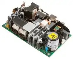


CHD250PS24
AC/DC Open Frame Power Supply (PSU), ITE & Medical, 1 Output, 250 W, 80V AC to 264V AC
- Manufacturer: XP POWER
- Product type: AC / DC Open Frame Power Supplies
- Product Range: CHD
- No. of Outputs: 1 Output
- Output Power Max: 250W
- Input Voltage VAC: 80V AC to 264V AC
- Input Voltage AC Max: 264V
- Input Voltage AC Min: 80V
- Power Supply Approvals: ITE & Medical
- Power Supply Output Type: Adjustable, Fixed
- Output Current - Output 1: 10.4A
- Output Voltage - Output 1: 24VDC
- Power Rating (Convection Cooling): 250W
| Delivery and price | |
|---|---|
| Units per pack | 10 |
| Price | 100.05 € |
| Current stock | 10+ |
| Lead time | 30 days |
XP Power

## 250 Watts

- 250 W Convection-cooled

- Industry Standard 3”x 5”Package

- 80 VAC to 300 VAC Input

- 5V Standby (optional)

- <0.5W Standby Power

- IT & Medical (BF) Safety Approvals

- Power Fail & Inhibit Signals

- 3 Year Warranty

Dimensions:

The universal AC input CHD250 provides 250W of convection cooled output power in a 3” x 5” industry standard package, over the temperature range -20°C to +50°C with derating to +70°C. Approved for IT and Medical and with a feature set including a 5V standby output, <0.5W input power when in standby mode, power fail and inhibit signals the CHD250 is ideal for a wide range of applications where fan cooling is not desirable.

CHD250: 5.00 x 3.00 x 1.43” (115 x 76 x 36 mm) CHD250-C: 5.50 x 3.48 x 1.75” (139.7 x 88.5 x 44.4 mm)

Models & Ratings

|Output Voltage 1|Output Current V1<br>Standby Supply V2<br>(optional)|Standby Supply V2<br>(optional)<br>Output Power|Model Number(1,2)|
|---|---|---|---|
|12 V|20.8 A<br>5.0 V / 0.5 A|5.0 V / 0.5 A<br>250 W|CHD250PS12|
|15 V|16.7 A<br>5.0 V / 0.5 A|5.0 V / 0.5 A<br>250 W|CHD250PS15|
|24 V|10.4 A<br>5.0 V / 0.5 A|5.0 V / 0.5 A<br>250 W|CHD250PS24|
|28 V|8.9 A<br>5.0 V / 0.5 A|5.0 V / 0.5 A<br>250 W|CHD250PS28|
|48 V|5.2 A<br>5.0 V / 0.5 A|5.0 V / 0.5 A<br>250 W|CHD250PS48|


## ~~**Notes**~~

_1. Add suffix ‘-C’ for cover version e.g. CHD250PS24-C (derating will be applicable, see derating curve fig. 8)._

_2. Add suffix -A for 5 V standby option or -AC for standby and cover options combined, (derating will be applicable, see derating curve fig. 8)._

_3. Cover kits available. Order part no.: CCB200-CHD250 CVR_

**==> picture [376 x 223] intentionally omitted <==**

**----- Start of picture text -----**<br>
ø0.14 (3.5) 5.00 ±0.02 (127.0 ±0.51)<br>thru in 4 positions [rti“‘CNCNCOCO#C#C(#(Y’’YSNYN’NY’NL L<br>L3 A<br>Output<br>C64 Voltage<br>Input Connector Control<br>CON1<br>(64.7)2.55 1 (76.2 ±0.51)3.00 ±0.02 -VE<br>C53<br>2<br>; aS "SS, T1 edz el @ & +VE<br>E<br>ro ee es i (2 EG, Output<br>Terminals<br>(5.71)0.22 (23.4)0.92 (5.71)0.22 Po 4.55 (115.5) M4 Screws in 2 positions.Torque to<br>8lbs-in<br>(90 cNm) max.<br>1.43 ±0.04  Pin 2 Pin 1<br>Bi; eae RLU aa (36.3 ±1.0) Pin 10 J H Pin 9<br>Detail A<br>Signals Connector CON4<br>10 Way JST B10B-PHDSS<br>Scale 3:1<br>**----- End of picture text -----**<br>


**www.xppower.com**

1

XP Power

## Input

|Characteristic<br>~~po~~|Minimum|Typical|Maximum|Units|Notes & Conditions|
|---|---|---|---|---|---|
|Input Voltage - Operating<br>~~po~~<br>~~a~~<br>~~**p**O~~|80<br>~~OG~~|115/230<br>~~OG~~|264<br>~~OG~~|VAC<br>~~GO~~|Derate output power < 90 VAC. See fig. 1<br>~~GO~~|
|Input Voltage - Fault Condition<br>~~**p**O~~|||300|VAC|5 seconds max|
|Input Frequency<br>~~**p**O~~|47|50/60|63<br>~~f~~|Hz<br>~~f~~|Agency approval, 47-63 Hz<br>~~f~~|
|Power Factor<br>~~eG~~|~~eG~~|>0.93<br>~~eG~~|~~eG~~|~~GO~~|EN61000-3-2 class A compliant<br>~~GO~~|
|Input Current - Full Load<br>~~eG~~<br>~~pf~~|~~eG~~<br>~~pf~~<br>~~**e**s~~|2.4/1.3<br>~~eG~~<br>~~pf~~|~~eG~~<br>~~pf~~|A<br>~~GO~~<br>~~pf~~|115/230 VAC<br>~~GO~~<br>~~pf~~|
|No Load Input Power|~~**e**s~~||0.5|W|All models, when inhibit activated|
||~~**e**s~~<br>~~es~~|3.2||W<br>~~G~~|CHD250PS12 - 115V AC<br>~~G~~|
||~~es~~<br>~~ee~~|3.1|~~O~~|W<br>~~G~~<br>~~O~~|CHD250PS12 - 230V AC<br>~~G~~<br>~~O~~|
||~~es~~<br>~~ee~~|3.8|~~O~~|W<br>~~O~~|CHD250PS24 - 115V AC<br>~~O~~|
||~~ee~~<br>~~a~~<br>~~es~~|3.1|~~O~~|W<br>~~O~~|CHD250PS24 - 230V AC<br>~~O~~|
||~~es~~|3.5||W|CHD250PS48 - 115V AC|
||~~es~~<br>~~GO~~|2.8<br>~~GO~~|~~GO~~|W<br>~~GO~~|CHD250PS48 - 230V AC<br>~~GO~~|
|Inrush Current<br>~~eG~~|~~GO~~<br>~~eG~~|20<br>~~GO~~|40<br>~~GO~~<br>~~GG~~|A<br>~~GO~~<br>~~GG~~|264 VAC cold start<br>~~GO~~<br>~~GG~~|
|Earth Leakage Current<br>~~OG~~|~~OG~~|85/170<br>~~OG~~|250<br>~~OG~~|μA<br>~~DO~~|Typ. 115/230 VAC 50 Hz, Max 264 VAC 60 Hz<br>~~DO~~|
|Input Protection<br>~~a~~|5 A/250 V internal fuse in both AC lines|||||


## **Input Voltage Derating**

Figure 1

|5 Seconds Maximum<br>200<br>150<br>50<br>100<br>250<br>Output Power (W)<br>300||
|---|---|
|80<br>85<br>300<br>90<br>264||
|Input Voltage (VAC)||
|Output||
|Characteristic<br>Minimum<br>Typical<br>Maximum<br>Units<br>Notes & Conditions<br>Output Voltage<br>12<br>48<br>VDC<br>See Models and Ratings table<br>~~po~~<br>~~Ge~~||
|Initial Set Accuracy<br>±1<br>%<br>50% load, 115/230 VAC<br>~~GG~~||
|Output Voltage Adjustment<br>+5/-4<br>%<br>~~Ge~~||
|Minimum Load<br>0<br>A<br>~~Ge~~||
|Start Up Delay<br>1.3<br>2.0<br>s<br>115/230 VAC full load from input AC turn on<br>~~a OG~~||
|Hold Up Time<br>15<br>ms<br>90 VAC, full load<br>Drift<br>±0.2<br>%<br>After 20 min warm up<br>Line Regulation<br>±0.5<br>%<br>90-264 VAC at 50% load<br>~~eG~~<br>~~dG~~<br>~~eG~~<br>~~OG~~||
|Load Regulation<br>±0.5<br>%<br>On V1, from 0-100% load<br>~~eG~~||
|Transient Response<br><4<br>%<br>Recovery within 1% in less than 500μs<br>for a 50-75%-50% load change<br>~~GO~~||
|Ripple & Noise<br>1<br>% pk-pk<br>20 MHz bandwidth<br>~~a OG~~||
|Overvoltage Protection<br>115<br>140<br>%<br>Vnom DC. Output 1, recycle input to reset<br>~~Ge~~||
|Overload Protection<br>110<br>150<br>%<br>Trip & Restart characteristic V1<br>Short Circuit Protection<br>Shutdown and auto recovery<br>Temperature Coefficient<br>0.05<br>%/˚C<br>Overtemperature Protection<br>Not fitted<br>Patient Leakage Current<br>83<br>100<br>μA<br>264 VAC/60 Hz<br>~~Ge~~<br>~~(ON~~<br>~~(OO~~<br>~~Ce~~<br>~~a~~<br>~~DD (OO~~<br>~~(OO~~<br>~~pT~~||


**www.xppower.com**

2

XP Power

## General

**==> picture [538 x 607] intentionally omitted <==**

**----- Start of picture text -----**<br>
Characteristic Minimum Typical Maximum Units Notes & Conditions<br>peGe Efficiency  93-94 % 230 VAC full load<br>Isolation: Input to Output  4000 VAC 2 x MOPP<br>Input to Ground Output to Ground  esRsesa 15001500  GGGe 45-280 VACVACkHz  1 X MOPP1 X MOPPPFC<br>a 31 kHz Boost<br>Switching Frequency<br>esa 56-9163 kHzkHz Main converterStandby (optional)<br>eG Power Density 11.7 W/in [3]<br>a Mean Time Between Failure GGG 213 kHrs  MIL-HDBK-217F, Notice 2 +25 °C GB<br>a 0.94 (425)0.97 (441) ee pT CHD250PSxxCHD250PSxx-A<br>Weight eea ee 1.36 (619) lb (g) pOpT CHD250PSxx-C<br>a 1.40 (636) pT CHD250PSxx-AC<br>Efficiency Vs Load<br>100.00%<br>Figure 2  90.00%<br>12 V Models<br>80.00%<br>70.00%<br>60.00%<br>50.00% PS12  115V<br>PS12  230V<br>40.00%<br>30.00%<br>20.00%<br>10.00%<br>0<br>20% 30% 40% 50% 60% 70% 80% 90% 100%<br>load %<br>Figure 3<br>24 V Models<br>100.00%<br>90.00%<br>80.00%<br>70.00%<br>60.00% PS24 115V<br>50.00% PS24 230V<br>40.00%<br>30.00%<br>20.00%<br>10.00%<br>0<br>20% 30% 40% 50% 60% 70% 80% 90% 100%<br>load %<br>Figure 4<br>48 V Models 100.00%<br>90.00%<br>80.00%<br>70.00%<br>60.00%<br>PS48 115V<br>50.00% i PS48 230V<br>40.00%<br>30.00%<br>20.00%<br>10.00%<br>0<br>20% 30% 40% 50% 60% 70% 80% 90% 100%<br>load %<br>Efficiency (%)<br>Efficiency (%)<br>Efficiency (%)<br>**----- End of picture text -----**<br>


**www.xppower.com**

3

XP Power

Signals & Controls Characteristic Notes & Conditions Uncommitted isolated optocoupler transistor, normally off when AC is good (see fig.5) Power Fail (AC-OK) Provides 5 ms warning of loss of output from AC failure off when AC is healthy. Inhibit Uncommitted isolated optocoupler diode, powered diode inhibits the supply (see fig.6 & 7) Standby Supply (optional) 5V/0.5A Isolated supply present when AC applied. Remote Sense Compensates for 0.25V per lead, 0.5V total drop. ~~—~~

**==> picture [496 x 200] intentionally omitted <==**

**----- Start of picture text -----**<br>
Power Fail Inhibit (High) Inhibit (Low)<br>Figure 5  Figure 6  Figure 7<br>5 V 5 V<br>POWER SUPPLY<br>POWER SUPPLY POWER SUPPLY<br>8V Max 3 mA Pin 2 CON 4Power Fail 5 mA    8 V Max 1K<br>Collector  Inhibit Hi  8 V Max<br>Pin 4 CON 4 Inhibit Hi<br>Transistor On: Input & Output Not OK Pin 4<br>Power Fail Transistor Off: Input & Output OK CON 4<br>Emitter<br>Pin 1 CON 4 Inhibit Lo Inhibit Lo<br>Pin 3 CON 4 5 mA Pin 3 CON 4<br>Signal Connector C 1 3 Pin 7 CON 4VI RTN x Signal Connector OX Pin 7 CON 4VI RTN Signal Connector<br>Environmental<br>**----- End of picture text -----**<br>


|Characteristic|Minimum|Typical|Maximum|Units|Notes & Conditions|
|---|---|---|---|---|---|
|Operating Temperature|-20||+70|°C|See derating curve, fig.8. and Thermal<br>Considerations on page 8.|
|Storage Temperature|-40||+85|°C||
|Cooling|||||Convection cooled|
|Humidity|||95|%RH|Non-condensing|
|Operating Altitude|||5000|m|Information Technology|
||||4000||Medical|
|Shock|±3 x 30g shocks in each plane, total 18 shocks. 30g = 11ms (±0.5msec), half sine. Conforms to EN60068-2-27 & EN60068-2-47|||||
|Vibration|Single axis 10 - 500 Hz at 2g sweep and endurance at resonance in all 3 planes. Conforms to EN60068-2-6|||||


## **Temperature Derating Curve**

**==> picture [528 x 151] intentionally omitted <==**

**----- Start of picture text -----**<br>
Figure 8<br>Standard & Covered (-C) versions 5 V Standby (-A & -AC) versions<br>300<br>Open Frame Convection<br>250217 220 Open Frame Convection<br>200 Covered Convection Covered Convection<br>165<br>125 126.5<br>108.5 110<br>82.5<br>0 PS 0<br>-20 50 70 -20 50 70<br>Ambient Temperature (°C) Ambient Temperature (°C)<br>Output Power (W) Output Power (W)<br>**----- End of picture text -----**<br>


**www.xppower.com**

4

|XP Power<br>**CHD250 Series**<br>**AC-DC Power Supplies**<br>EMC: Emissions<br>Phenomenon<br>Standard<br>Test Level<br>Notes & Conditions<br>Conducted<br>EN55032/11<br>Class B<br>Radiated<br>EN55032/11<br>Class A<br>Class B<br>With 2 turn Wurth 742-700-56 core or similar<br>on AC cable<br>Harmonic Current<br>EN61000-3-2<br>Class A<br>All models<br>EMC: Immunity<br>Phenomenon<br>Standard<br>Test Level<br>Criteria<br>Notes & Conditions<br>~~—<~~|XP Power<br>**CHD250 Series**<br>**AC-DC Power Supplies**<br>EMC: Emissions<br>Phenomenon<br>Standard<br>Test Level<br>Notes & Conditions<br>Conducted<br>EN55032/11<br>Class B<br>Radiated<br>EN55032/11<br>Class A<br>Class B<br>With 2 turn Wurth 742-700-56 core or similar<br>on AC cable<br>Harmonic Current<br>EN61000-3-2<br>Class A<br>All models<br>EMC: Immunity<br>Phenomenon<br>Standard<br>Test Level<br>Criteria<br>Notes & Conditions<br>~~—<~~|XP Power<br>**CHD250 Series**<br>**AC-DC Power Supplies**<br>EMC: Emissions<br>Phenomenon<br>Standard<br>Test Level<br>Notes & Conditions<br>Conducted<br>EN55032/11<br>Class B<br>Radiated<br>EN55032/11<br>Class A<br>Class B<br>With 2 turn Wurth 742-700-56 core or similar<br>on AC cable<br>Harmonic Current<br>EN61000-3-2<br>Class A<br>All models<br>EMC: Immunity<br>Phenomenon<br>Standard<br>Test Level<br>Criteria<br>Notes & Conditions<br>~~—<~~|XP Power<br>**CHD250 Series**<br>**AC-DC Power Supplies**<br>EMC: Emissions<br>Phenomenon<br>Standard<br>Test Level<br>Notes & Conditions<br>Conducted<br>EN55032/11<br>Class B<br>Radiated<br>EN55032/11<br>Class A<br>Class B<br>With 2 turn Wurth 742-700-56 core or similar<br>on AC cable<br>Harmonic Current<br>EN61000-3-2<br>Class A<br>All models<br>EMC: Immunity<br>Phenomenon<br>Standard<br>Test Level<br>Criteria<br>Notes & Conditions<br>~~—<~~|
|---|---|---|---|
||Low Voltage PSU EMC<br>EN61204-3<br>High severity level||as below|
||Radiated<br>EN61000-4-3<br>3||A|
||EFT<br>EN61000-4-4<br>3||A|
||Surges<br>EN61000-4-5<br>Installation class 3||A|
||Conducted<br>EN61000-4-6<br>3||A|
||Int >95%(0 VAC),8.3ms||A|
||EN55035 (100 VAC)<br>Dip 30% (70 VAC), 416ms||B|
||Int >95% (0 VAC), 4160ms||B|
||Int >95% (0 VAC), 10.0ms||A|
||EN55035 (240 VAC)<br>Dip 30% (168 VAC), 500ms||B|
||Int >95% (0 VAC), 5000ms||B|
||Int >95% (0 VAC), 10.0ms||A|
||Dips and Interruptions<br>EN60601-1-2 (100 VAC)<br>Dip 60% (40 VAC), 100ms<br>Dip 30% (70 VAC), 500ms||A<br>Derate output power to 120 W<br>A|
||Int >95% (0 VAC), 5000ms||B|
||Int >95% (0 VAC), 10.0ms||A|
||EN60601-1-2 (240 VAC)<br>Dip 60% (96 VAC), 100ms<br>Dip 30% (168 VAC), 500ms||A<br>A|
||Int >95% (0 VAC), 5000ms||B|
|Safety Approvals<br>Safety Certification<br>Safety Standard<br>Notes & Conditions<br>CB Report<br>IEC60950-1:2005, IEC62368-1:2014<br>Information Technology<br>IEC60601-1 Ed 3 Including Risk Management<br>Medical<br>UL<br>UL60950-1 (2014), CSA 22.2 No.60950-1-1:08,<br>UL62368-1:2014, CSA C22.2 No62368-1-14<br>Information Technology<br>ANSI/AAMI ES60601-1:2005 & CSA C22.2, No.60601-1:08<br>Medical<br>EN<br>EN60950-1, EN62368-1:2014+A11:2017<br>Information Technology<br>EN60601-1<br>Medical<br>Equipment Protection Class<br>Class I & BF<br>See safety agency conditions of acceptibility for details<br>CE<br>Meets all applicable directives<br>UKCA<br>Meets all applicable legislation<br>~~=——~~||||
|Means of Protection<br>Category<br>Primary to Secondary<br>2 x MOPP (Means of Patient Protection)<br>IEC60601-1 Ed 3<br>Primary to Earth<br>1 x MOPP (Means of Patient Protection)<br>Secondary to Earth<br>1 x MOPP (Means of Patient Protection)<br>~~es~~||||


**www.xppower.com**

5

XP Power

## **CHD250**

**==> picture [534 x 484] intentionally omitted <==**

**----- Start of picture text -----**<br>
ø0.14 (3.5) 5.00 ±0.02 (127.0 ±0.51)<br>thru in 4 positions<br>L3 A<br>Output<br>C64 Voltage<br>Input Connector Control<br>CON1<br>2.55 3.00 ±0.02<br>(64.7) 1 (76.2 ±0.51) -VE<br>C53<br>2<br>T1 +VE In put Connector CON 1<br>E 1 Line<br>——7aS ee B rice = apeZ MetteYe sokls : TerminalsOutput  — 2 Neutral<br>M4 Screws in<br>0.22 0.92 0.22 Po 2 positions. Mates with Molex housing<br>(5.71) (23.4) (5.71) 4.55 (115.5) Torque to  09-50-1031 and Molex<br>8lbs-in  series 5194 crimp terminals.<br>(90 cNm) max.<br>Output Connector CON 3<br>1 +VE<br>1.43 ±0.04  Pin 2 Pin 1<br>(36.3 ±1.0) 2 -VE<br>Signals Connector CON 4<br>Pin 10 Pin 9 1 Power Fail (Emitter)<br>2 Power Fail (Collector)<br>Detail A<br>Signals Connector CON4 3 Inhibit (Cathode)<br>CHD250 Standby Option (-A)  10 Way JST B10B-PHDSSScale 3:1 4 Inhibit (Anode)<br>5 N/C<br>ø0.14 (3.5)<br>thru in 4 positions 6 N/C<br>7 - VE Sense<br>5.00 ±0.02 (127.0 ±0.51) 0.30 (7.5)<br>8 - VE Sense<br>9 +VE Sense<br>A<br>L3 10 +VE Sense<br>A Output<br>C64 C53 under  Voltage  Mates with JST PHDR-<br>standby board Control 10VS housing and JST<br>_ (64.7)2.55 SN in ames, Standby Le B -VE SPHD-001T-P0.5 crimp terminals<br>Board<br>T1 3.00 ±0.02(Option -A) 37.8)1.49 +VE Standby Output (Option -A)<br>(76.2 ±0.51)<br>Output  1 +5 V<br>Terminals<br>iH (5.71)0.22 (23.4)0.92 (5.71)0.22 Filiee oilsia 4.55 (115.5) Mu cilan (20.2)0.80 Pin 4 M4 Screws in 2 positions.Torque to 8lbs-in  234 +5 V0 V0 V<br>Pin 3 (90 cNm) max.<br>Mates with JST PHR-4<br>Pin 2<br>housing and JST<br>Pin 1 SPH-002T-P0.5L crimp<br>1.43 ±0.04  terminals<br>(36.3 ±1.0) Detail B<br>Standby Board O/P<br>Connector Cons<br>JST S4B-PH-K-S<br>**----- End of picture text -----**<br>


## **CHD250 Standby Option (-A)**

## ~~**Notes**~~

1. Dimensions shown in inches (mm).

**www.xppower.com**

6

XP Power

**==> picture [539 x 564] intentionally omitted <==**

**----- Start of picture text -----**<br>
M3 Mounting Holes<br>CHD250 Covered (-C) in 2 positions<br>0.39 4.72 (120.0)<br>(9.85) / Pin 2 Pin 1<br>Pin 10 Pin 9<br>0.93<br>(23.7) e Signals Connector CON4Detail A<br>10 way JST B10B-PHDSS<br>1.75 (44.4) 5.50 ±0.02 (139.7 ±0.5) _ 0.59 (15.0)<br>Con 4<br>=aan A Output Voltage Control<br>Con 1 =| | 12 Looepres Fitm 3.48 ±0.02 (88.5 ±0.5)(43.9)1.73 Toe=ra SES -VE+VE > Con 3M4 Screws in 2 positionstorque to 8 lbs Output Terminals  12In put Connector CON 1NeutralLine<br>= H ee co as 1.03 TIE (90 cNm) max.<br>(26.1) Mates with Molex housing<br>[im7 | B ine eeRonnHereESce su Con 2 09-50-1031 and Molex<br>0.39 4.72 (120.0) series 5194 crimp terminals.<br>(9.85)<br>i<br>M3 mounting holes in 4 positions<br>| | o 4 | 3.0 mm from bottom face of covermaximum penetration by screw to be Output Connector CON 3<br>1 +VE<br>1.97 2 -VE<br>(50.0)<br>Signals Connector CON 4<br>y 1 Power Fail (Emitter)<br>° ° 2 Power Fail (Collector)<br>0.7<br>(19.3) 3 Inhibit (Cathode)<br>4 Inhibit (Anode)<br>CHD250 Covered Standby Option (-AC)  5 N/C<br>6 N/C<br>M3 Mounting Holes<br>in 2 positions 7 - VE Sense<br>0.39 4.72 (120.0)<br>(9.85) Pin 2 Pin 1 8 - VE Sense<br>9 +VE Sense<br>J 10 +VE Sense<br>(23.7)0.93 / = Pin 10Signals Connector CON4 C N ath Detail A E Pin 9 Mates with JST PHDR-<br>10 way JST B10B-PHDSS 10VS housing and JST<br>kK 1.75 (44.4) 5.50 ±0.02 (139.7 ±0.5) 0.59 (15.0) SPHD-001T-P0.5 crimp terminals<br>= AS A 5 Con 4Output Voltage Control Standby Output<br>a<br>| HHS 4) Con 3 (Option -A)<br>Con 1 =_||h 12 Loeeeeeoe teIq)a 3.48 ±0.02 (88.5 ±0.5)(43.9)1.73 ' (i=ve B see -VE+VE S M4 Screws in 2 positionstorque to 8 lbs (90 cNm) max.Output Terminals  123 +5 V+5 V0 V<br>lm » 1.03 aa 4 0 V<br>(26.1)<br>=7f | comDBo a settOiseenn ee e o u | a) : | Con 2 Mates with JST PHR-4<br>0.39 4.72 (120.0) —_ housing and JST<br>(9.85) = M3 mounting holes in 4 positionsmaximum penetration by screw to be SPH-002T-P0.5L crimp terminals<br>F | 2il | 3.0 mm from bottom face of cover<br>1.97<br>(50.0)<br>- °<br>0.7<br>(19.3)<br>**----- End of picture text -----**<br>


## ~~**Notes**~~

1. Dimensions shown in inches (mm).

**www.xppower.com**

7

XP Power

## Thermal Considerations ~~rr~~

In order to ensure safe operation of the PSU in the end-use equipment, the temperature of the components listed in the table below must not be exceeded. Temperature should be monitored using thermocouples placed on the hottest part of the component (out of direct air flow). See below for component locations.

|Temperature Measurements (At Ambient 50 °C)|Temperature Measurements (At Ambient 50 °C)|
|---|---|
|Component|Max Temperature °C|
|T1 Coil|120 ° C|
|L3 Coil|120 ° C|
|C64|105 ° C|
|C53|105 ° C|


Service Life ~~#8#838}3}§}§}§}= kk XX =~~ The estimated service life of the CHD250 Series is determined by the cooling arrangements and load conditions experienced in the end application. Due to the uncertain nature of the end application this estimated service life is based on the actual measured temperature of a key capacitors with in the product when installed by the end application. The worst case of the two figures should be taken as the indicative service life in 24/7 operation.

The graph below expresses the estimated lifetime of a given component temperature and assumes continuous operation at this temperature.

## **Estimated Service Life vs Component Temperature**

**==> picture [520 x 278] intentionally omitted <==**

**----- Start of picture text -----**<br>
350000<br>300000<br>250000<br>200000<br>150000<br>100000<br>50000<br>0 L3<br>105 95 85 75 65 55<br>C64<br>C53 Temperature (°C)<br>a lew ec e<br>180000 C53<br>160000<br>140000 T1<br>120000<br>100000 TOC<br>fh".<br>80000<br>60000<br>40000<br>20000<br>0<br>105 95 85 75 65 55<br>C64 Temperature (°C)<br>Lifetime (Hrs)<br>Lifetime (Hrs)<br>**----- End of picture text -----**<br>


**www.xppower.com**

07 December 2023
Updated at February 9, 2023
XP Power is a globally recognized leader in the design and manufacture of critical power solutions for the electronics industry. With a steadfast commitment to total quality and in-house engineering expertise, the company delivers highly reliable components that support complex applications across the industrial, healthcare, and technology sectors. Their extensive manufacturing capabilities provide engineers with a broad and dependable source for innovative power products. Our extensive portfolio of XP Power components is heavily focused on robust power and line protection. The core of this offering features a vast selection of high-performance AC/DC converters, designed to meet the rigorous efficiency and footprint demands of modern electronic systems. Complementing these are numerous reliable DC/DC converters, providing versatile options for precise voltage regulation and seamless system integration. Beyond their primary power conversion ranges, XP Power manufactures specialized components to address specific design challenges. Our selection includes essential passive components, such as power line filters for effective EMC and RFI suppression, ensuring signal integrity and strict regulatory compliance. Additionally, we provide dedicated AC/DC LED power supplies tailored for reliable, long-lasting performance in advanced commercial and industrial lighting applications.
About Novapart
Novapart is a B2B electronic component broker specialising in stock shortages and cost reduction. We source hard-to-find parts and identify compliant alternatives across a catalogue of 410,000+ components from 500+ manufacturers.
Learn more →Stock Shortage Specialist
When a component is unavailable, discontinued or has an unacceptable lead time, we tap into our network of vetted European and Asian distributors to source what you need — without compromising on quality or traceability.
Request a quote →Compliant Alternatives
We identify pin-to-pin, electrically equivalent substitutes that meet the same certifications (RoHS, AEC-Q100, REACH) as your original specification — validated against datasheets, not just part numbers. Often at a lower cost.
BOM Analysis service →