
Image not available
Illustrative purposes only

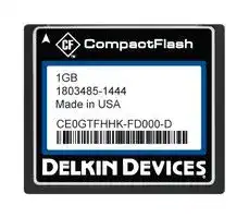
CE0GTFHHK-FD000-D
MEMORY CARD, COMPACTFLASH, SLC, 1GB
⚠️ Reference pricing provided. In case of supply shortages, we will connect you with our trusted procurement partners to ensure your project's continuity.
- Manufacturer: DELKIN DEVICES
- Product type: Flash Memory Cards
- Product Range: C400 Series
- Memory Capacity: 1GB
- Blank Media Flash Memory Type: Compact Flash Card, Type I
| Delivery and price | |
|---|---|
| Units per pack | 50 |
| Price | 30.03 € |
| Current stock | 10+ |
| Lead time | 30 days |
Datasheet

C400 & C400 ELC Series SLC Industrial CompactFlash L5ENG00049 Rev. D ## **C400 & C400 ELC SLC Industrial CompactFlash Engineering Specification** **Document Number L5ENG00049** **Revision: D** **==> picture [183 x 29] intentionally omitted <==** **----- Start of picture text -----**<br> WO AGE<br>| ae<br>**----- End of picture text -----**<br> © 2016 | Delkin Devices Inc. C400 & C400 ELC Series SLC Industrial CompactFlash L5ENG00049 Rev. D ## **Table of Contents** |1.0|Product Overview ............................................................................................................ 6| |---|---| |1.1|Capacities and Part Numbers .................................................................................................................. 8| |1.2|C400 ELC (Extended Life Cycle) Series ................................................................................................. 9| |1.2.1<br>ELC Capacities and Part Numbers .................................................................................................. 9|| |1.3|Mechanical Specifications ..................................................................................................................... 10| |1.4|Dimensions ............................................................................................................................................ 10| |2.0|Product Specifications .................................................................................................. 11| |2.1|System Performance ............................................................................................................................. 11| |2.2|Reliability ............................................................................................................................................... 11| |2.3|Environmental Specifications ................................................................................................................ 11| |2.4|CHS Parameters .................................................................................................................................... 12| |3.0|CF Card Interface ......................................................................................................... 13| |3.1|Card Pin Assignment ............................................................................................................................. 13| |3.2|Card Pin Explanation ............................................................................................................................. 15| |4.0|Electrical Interface ........................................................................................................ 19| |4.1|Absolute Maximum Conditions .............................................................................................................. 19| |4.2|Input Power ............................................................................................................................................ 19| |4.3|Input Leakage Current ........................................................................................................................... 19| |4.4|Input Characteristics .............................................................................................................................. 20| |4.5|Output Drive Type .................................................................................................................................. 20| |4.6|Output Drive Characteristics .................................................................................................................. 20| |4.7|Interface/Bus Timing .............................................................................................................................. 20| |4.8|Attribute Memory Read Timing .............................................................................................................. 21| |4.9|Configuration Register (Attribute Memory) Write Timing ....................................................................... 22| |4.10|Common Memory Read Timing ............................................................................................................. 23| |4.11|Common Memory Write Timing ............................................................................................................. 24| |4.12|I/O Input (Read) Timing ......................................................................................................................... 25| |4.13|I/O Input (Write) Timing ......................................................................................................................... 26| |4.14|True IDE PIO Mode Read/Write Timing ................................................................................................ 27| |4.15|True IDE Multiword DMA Mode Read/Write Timing .............................................................................. 29| |5.0|Card Configuration ........................................................................................................ 31| |5.1|Delkin Card Configuration ..................................................................................................................... 31| |5.2|Attribute Memory Function .................................................................................................................... 33| |5.3|Configuration Option Register (Address 200H in Attribute Memory) .................................................... 34| |5.4|Card Configuration and Status Register (Address 200H in Attribute Memory) ..................................... 35| |5.5|Pin Replacement Register (Address 200H in Attribute Memory) .......................................................... 35| |5.6|Socket and Copy Register (Address 200H in Attribute Memory) .......................................................... 36| |6.0|Transfer Functions ........................................................................................................ 38| |6.1|Input/Output ........................................................................................................................................... 38| |6.2|Common Memory .................................................................................................................................. 39| |6.3|True IDE Mode I/O ................................................................................................................................. 39| © 2016 | Delkin Devices Inc. 2 C400 & C400 ELC Series SLC Industrial CompactFlash |& C400ELC Series SLCIndustrialCompactFlash<br>L5ENG00049Rev. D| |---| |7.0<br>Software Interface ......................................................................................................... 41| |7.1<br>CF-ATA Drive Register Set Definition and Protocol .............................................................................. 41| |7.2<br>I/O Primary and Secondary Address Configurations ............................................................................. 41| |7.3<br>Contiguous I/O Mapped Addressing ...................................................................................................... 42| |7.4<br>Memory Mapped Addressing ................................................................................................................. 43| |7.5<br>True IDE Mode Addressing ................................................................................................................... 45| |7.6<br>CF-ATA Registers .................................................................................................................................. 45| |7.6.1<br>Data Register (Address – 1F0H[170H];Offset 0,8,9) ..................................................................... 45| |7.6.2<br>Error Register (Address – 1F1H [171H]; Offset 1, 0DH Read Only) ............................................. 47| |7.6.3<br>Feature Register (Address – 1F1H[171H]; Offset 1, 0DH Write Only) .......................................... 47| |7.6.4<br>Sector Number (LBA 7-0) Register (Address – 1F3H[173H]; Offset 3) ......................................... 47| |7.6.5<br>Cylinder Low (LBA 15-8) Register (Address – 1F4H[174H]; Offset 4) .......................................... 47| |7.6.6<br>Cylinder High (LBA 23-16) Register (Address – 1F5H[175H]; Offset 5) ....................................... 47| |7.6.7<br>Drive/Head (LBA 27-24) Register (Address 1F6H[176H]; Offset 6) .............................................. 47| |7.6.8<br>Drive/Head (LBA 27-24) Register (Address 1F6H[176H]; Offset 6) .............................................. 48| |7.6.9<br>Status & Alternate Status Registers (Address 1F7H[177H]&3F6H[376H]; Offsets 7 & E) ............ 49| |7.6.10<br>Device Control Register (Address – 3F6H[376H]; Offset E) ......................................................... 49| |7.6.11<br>Card (Drive) Address Register (Address – 3F7H[377H]; Offset F) ............................................... 50| |7.7<br>CF-ATA Command Description ............................................................................................................. 52| |7.7.1<br>CF-ATA Command set .................................................................................................................. 52| |7.7.2<br>Check Power Mode – 98H or E5H ................................................................................................ 54| |7.7.3<br>Execute Drive Diagnostics – 90H .................................................................................................. 55| |7.7.4<br>Erase Sector(s) – C0H ................................................................................................................... 56| |7.7.5<br>Flush Cache – E7h ........................................................................................................................ 56| |7.7.6<br>Format Track – 50H ....................................................................................................................... 57| |7.7.7<br>Identify Drive - ECH ....................................................................................................................... 57| |7.7.7.1<br>General Configuration ............................................................................................................ 59| |7.7.7.2<br>Default Number of Cylinders.................................................................................................. 59| |7.7.7.3<br>Default Number of Heads ...................................................................................................... 59| |7.7.7.4<br>Default Number of Sectors per Track .................................................................................... 59| |7.7.7.5<br>Number of Sectors per Card .................................................................................................. 59| |7.7.7.6<br>Serial Number ........................................................................................................................ 59| |7.7.7.7<br>ECC Count ............................................................................................................................. 59| |7.7.7.8<br>Firmware Revision ................................................................................................................. 59| |7.7.7.9<br>Model Number ....................................................................................................................... 60| |7.7.7.10<br>Read/Write Multiple Sector Count ......................................................................................... 60| |7.7.7.11<br>Capabilities ............................................................................................................................ 60| |7.7.7.12<br>PIO Data transfer Cycle Timing Mode ................................................................................... 60| |7.7.7.13<br>Translation Parameters Valid ................................................................................................ 60| |7.7.7.14<br>Current Number of Cylinders, Heads, Sectors/Track ............................................................ 60| |7.7.7.15<br>Current Capacity .................................................................................................................... 60| |7.7.7.16<br>Multiple Sector Setting ........................................................................................................... 60| |7.7.7.17<br>Total Sectors Addressable in LBA Mode ............................................................................... 61| © 2016 | Delkin Devices Inc. 3 C400 & C400 ELC Series SLC Industrial CompactFlash L5ENG00049 Rev. D |7.7.7.18<br>Multiword DMA transfer ......................................................................................................... 61|7.7.7.18<br>Multiword DMA transfer ......................................................................................................... 61| |---|---| |7.7.7.19<br>Advanced PIO transfer modes supported ............................................................................. 61|| |7.7.7.20<br>Minimum Multiword DMA transfer cycle time ........................................................................ 61|| |7.7.7.21<br>Recommended Multiword DMA transfer cycle time............................................................... 62|| |7.7.7.22<br>Minimum PIO transfer cycle time without flow control ........................................................... 62|| |7.7.7.23<br>Minimum PIO transfer cycle time with IORDY ....................................................................... 62|| |7.7.7.24<br>Security Status ....................................................................................................................... 62|| |7.7.8|Idle – 97H or E3H .......................................................................................................................... 63| |7.7.9|Idle Immediate – 95H or E1H ........................................................................................................ 64| |7.7.10|Initialize Drive Parameters – 91H .................................................................................................. 64| |7.7.11|Key Management Structure Read – B9h (Feature: 0-127) ............................................................ 65| |7.7.12|Key Management Read Keying Material - B9h (Feature: 80) ....................................................... 65| |7.7.13|Key Management Change Key Management Value – B9h (Feature: 81) ..................................... 66| |7.7.14|NOP - 00h ...................................................................................................................................... 66| |7.7.15|Read Buffer – E4H ......................................................................................................................... 67| |7.7.16|Read DMA – C8h ........................................................................................................................... 67| |7.7.17|Read Long Sector - 22h or 23h ..................................................................................................... 68| |7.7.18|Read Multiple – C4H ...................................................................................................................... 69| |7.7.19|Read Sector(s) – 20H or 21H ........................................................................................................ 70| |7.7.20|Read Verify Sector(s) – 40H or 41H .............................................................................................. 71| |7.7.21|Recalibrate – 1XH .......................................................................................................................... 71| |7.7.22|Request Sense – 03H .................................................................................................................... 72| |7.7.23|Security Disable Password - F6h .................................................................................................. 73| |7.7.24|Security Erase Prepare - F3h ........................................................................................................ 74| |7.7.25|Security Erase Unit - F4h............................................................................................................... 74| |7.7.26|Security Freeze Lock - F5h............................................................................................................ 75| |7.7.27|Security Set Password - F1h ......................................................................................................... 75| |7.7.28|Security Unlock - F2h .................................................................................................................... 76| |7.7.29|Seek – 7XH .................................................................................................................................... 76| |7.7.30|Set Feature – EFH ......................................................................................................................... 77| |7.7.31|Set Multiple Mode – C6H ............................................................................................................... 78| |7.7.32|Set Sleep Mode – 99H or E6H ...................................................................................................... 79| |7.7.33|Standby – 96H or E2H ................................................................................................................... 79| |7.7.34|Standby – 94H or E0H ................................................................................................................... 80| |7.7.35|Translate Sector – 87H .................................................................................................................. 80| |7.7.36|Wear Level – F5H .......................................................................................................................... 81| |7.7.37|Write Buffer – E8H ......................................................................................................................... 82| |7.7.38|Write DMA – CAh .......................................................................................................................... 82| |7.7.39|Write Long Sector – 32H or 33H ................................................................................................... 83| |7.7.40|Write Multiple Command – C5H .................................................................................................... 84| |7.7.41|Write Multiple without Erase – CDH .............................................................................................. 85| |7.7.42|Write Sector(s) – 30H or 31H ........................................................................................................ 85| |7.7.43|Write Sector(s) without Erase – 38H ............................................................................................. 86| |7.7.44|Write Verify – 3CH ......................................................................................................................... 86| |7.8<br>Error Posting .......................................................................................................................................... 87|| © 2016 | Delkin Devices Inc. 4 C400 & C400 ELC Series SLC Industrial CompactFlash L5ENG00049 Rev. D |8.0<br>Comparing CF-ATA to PC Card-ATA and True IDE ..................................................... 90|8.0<br>Comparing CF-ATA to PC Card-ATA and True IDE ..................................................... 90| |---|---| |8.1<br>Electrical Differences ............................................................................................................................. 90|| |8.1.1|TTL Compatibility ........................................................................................................................... 90| |8.1.2|Pull Up Resistor Input Leakage Current ........................................................................................ 90| |8.2<br>Functional Differences ........................................................................................................................... 90|| |8.2.1|Additional Set Features Codes in CF-ATA .................................................................................... 90| |8.2.2|Additional Commands in CF-ATA .................................................................................................. 90| |8.2.3|Idle Timer ....................................................................................................................................... 90| |8.2.4|Recovery from Sleep Mode ........................................................................................................... 91| |9.0<br>SMART Feature Set ...................................................................................................... 92|| |9.1<br>SMART Data Structure .......................................................................................................................... 92|| |9.2<br>SMART Attribute Entries (Bytes 2 – 361 in SMART Data Structure) .................................................... 93|| |9.2.1|Spare Block Count Attribute .......................................................................................................... 93| |9.2.2|Erase Count Attribute .................................................................................................................... 94| |9.2.3|Total ECC Errors Attribute ............................................................................................................. 94| |9.2.4|Correctable ECC Errors Attribute .................................................................................................. 95| |9.2.5|Total Number of Reads Attribute ................................................................................................... 95| |9.2.6|UDMA CRC Errors Attribute .......................................................................................................... 95| ## **Table of Figures** Figure 1. CF Card Dimensions ............................................................................................... 10 Figure 2. Attribute Memory Read Timing Diagram .................................................................. 21 Figure 3. Configuration Register (Attribute Memory) Write Timing Diagram ........................... 22 Figure 4. Common Memory Read Timing Diagram ................................................................ 23 Figure 5. Common Memory Write Timing Diagram ................................................................. 24 Figure 6. I/O read Timing Diagram ......................................................................................... 25 Figure 7. I/O Write Timing Diagram ........................................................................................ 26 Figure 8. True IDE PIO Mode Read/Write Timing Diagram .................................................... 28 Figure 9. True IDE Multiword DMA Mode Read/Write Timing Diagram .................................. 30 © 2016 | Delkin Devices Inc. 5 C400 & C400 ELC Series SLC Industrial CompactFlash L5ENG00049 Rev. D ## **1.0 Product Overview** Delkin Devices’ C400 and C400 ELC Series SLC Industrial CompactFlash memory cards feature significant performance upgrades for industrial applications. These cards have superior features such as: - Advanced Wear Leveling - ECC error correction - Up to 50 MB/sec sustained write speed* - ° - -40 to 85 C Industrial operating temperature range - Compliant with CompactFlash Specification Rev. 4.1 - Operating modes – Memory, PCMCIA I/O, True IDE (PIO6 & MDMA4) IDE UDMA4 - Compliant with European Union Directive 2011/65/EU (ROHS 2-2.4) & GB/T 265722011 (China ROHS 2) - Shock: 40g’s at 11ms, MIL-STD-810, Method 516.6 - Vibration: 15Hz to 2,000Hz, MIL-STD-810, Method 514.5 - Humidity: 95% R-H, MIL-STD-810, Method 507.4 - Altitude: 80,000 feet - Capacities supported: - C400 Series: 128MB, 256MB, 512 MB, 1GB, 2GB, 4GB, 8GB and 16GB (64MB can be supplied as a 128MB formatted to 64MB) - C400 ELC Series: 128MB, 256MB, 512 MB, 1GB, 2GB & 4GB - NAND Single Level Cell flash (SLC) - Supports 3.3-Volt and 5-Volt operation - Fixed Drive and Removable configurations available - Available upon request – Custom CHS, mechanical features, labels and packaging - All capacity configurations are available with optional proprietary conformal coating *Dependent on host configuration and testing equipment. © 2016 | Delkin Devices Inc. 6 C400 & C400 ELC Series SLC Industrial CompactFlash L5ENG00049 Rev. D The C400 and C400 ELC Series SLC Industrial CompactFlash cards are manufactured in the USA at our own facilities in Poway, California. The cards are supported by Delkin’s lockeddown Bill of Materials that ensures consistent product performance and future compatibility. Delkin’s Industrial line of CompactFlash is the perfect solution for enterprises demanding specific higher qualitative and performance functions in a widely accepted, time-tested form factor. ## **Applications:** - Industrial Computers - Embedded Systems - Data Acquisition - Automotive - Flight Systems ● Agriculture - Manufacturing ● Gaming - Military ● Locomotive - Telecommunications ## **Optional Conformal Coating** Delkin’s proprietary conformal coating defends data integrity in harsh environments. Delkin utilizes an acrylic material that thoroughly covers exposed board and component surfaces with a protective coating. This process shields memory electronics from moisture and contamination, preventing metal corrosion and insulating conductors against electrical leakage. The coating also ruggedizes devices against the vibration, shock, and thermal stress of severe-service applications. Conformal coating is available as an option for Delkin industrial flash memory products in many form factors, including solid state drives, CompactFlash, Secure Digital, removable and embedded USB, PCMCIA, and mSATA © 2016 | Delkin Devices Inc. 7 C400 & C400 ELC Series SLC Industrial CompactFlash L5ENG00049 Rev. D ## **1.1 Capacities and Part Numbers** Delkin Devices C400 Series SLC Industrial CompactFlash cards are available in the following capacities and product grades: |Capacity|Product Grade|Part Number| |---|---|---| |128MB|SLC Industrial (-40 to 85°C)|CE12TFJHK-zz000-D| |256MB|SLC Industrial (-40 to 85°C)|CE25TFKHK-zz000-D| |512MB|SLC Industrial (-40 to 85°C)|CE51TFLHK-zz000-D| |1GB|SLC Industrial (-40 to 85°C)|CE0GTFHHK-zz000-D| |2GB|SLC Industrial (-40 to 85°C)|CE02TFNHK-zz000-D| |4GB|SLC Industrial (-40 to 85°C)|CE04TFNHK-zz000-D| |8GB|SLC Industrial (-40 to 85°C)|CE08TFPHK-zz000-D| |16GB|SLC Industrial (-40 to 85°C)|CE16TFPHK-zz000-D| ## zz: Drive configuration XX = removable/DMA & UDMA On FD = fixed disk/DMA & UDMA On X1 = removable/DMA & UDMA Off X2 = removable /DMA On/ UDMA Off F1 = fixed disk/DMA & UDMA Off F2 = fixed disk /DMA On/ UDMA Off For optional conformal coating, replace the 000 with 050. The CompactFlash cards are manufactured at our facilities in Poway, California USA. Many custom configurations are available including custom CHS, mechanical features, labels and packaging. Contact Delkin for information on 64MB cards. Refer to Section 1.2 for Extended Life Cycle (ELC) part numbers and details. © 2016 | Delkin Devices Inc. 8 C400 & C400 ELC Series SLC Industrial CompactFlash L5ENG00049 Rev. D ## **1.2 C400 ELC (Extended Life Cycle) Series** Delkin Devices’ C400 ELC (Extended Life Cycle) product line is aimed at applications requiring product stability for three, five or more years, utilizing long-life cycle flash and controller components. As opposed to consumer-grade solutions that can change every 3 – 6 months, Delkin will deliver the same controlled storage solution for the life of your project, eliminating costly re-qualifications. ELC products are ideal for medical, military, automotive & other industrial applications with extended product life cycles and stringent change management protocols. ## **1.2.1 ELC Capacities and Part Numbers** |Capacity|Product Grade|Part Number| |---|---|---| |128MB|SLC Industrial (-40 to 85°C)|CE12MJBHS-zz000-5| |256MB|SLC Industrial (-40 to 85°C)|CE25MJBHS-zz000-5| |512MB|SLC Industrial (-40 to 85°C)|CE51MJBHS-zz000-5| |1GB|SLC Industrial (-40 to 85°C)|CE0GMHWHS-zz000-5| |2GB|SLC Industrial (-40 to 85°C)|CE02MHWHS-zz000-5| |4GB|SLC Industrial (-40 to 85°C)|CE04MHWHS-zz000-5| ## zz: Drive configuration XX = removable/DMA & UDMA On FD = fixed disk/DMA & UDMA On X1 = removable/DMA & UDMA Off X2 = removable /DMA On/ UDMA Off F1 = fixed disk/DMA & UDMA Off F2 = fixed disk /DMA On/ UDMA Off For optional conformal coating, replace the 000 with 050. © 2016 | Delkin Devices Inc. 9 C400 & C400 ELC Series SLC Industrial CompactFlash L5ENG00049 Rev. D ## **1.3 Mechanical Specifications** Delkin Devices SLC Commercial and Industrial cards are Type I CompactFlash cards. ## **1.4 Dimensions** |**1.4 Dimensions**|| |---|---| |Length:|36.4 ± 0.15 mm (1.433 ±.006 in.)| |Width:|42.80 ± 0.10 mm (1.685 ±.004 in.)| |Thickness Including<br>Label Area:|3.3 mm ± 0.10 mm (.130 ± .004 in.)| |Weight:|12.0 g typical| **Figure 1. CF Card Dimensions** © 2016 | Delkin Devices Inc. 10 C400 & C400 ELC Series SLC Industrial CompactFlash L5ENG00049 Rev. D ## **2.0 Product Specifications** ## **2.1 System Performance** |Parameter|Value| |---|---| |Data Transfer Rate|Upto 70 MB/s| |Sustained Read|Upto 70 MB/s| |Sustained Write|Upto 50 MB/s| **Note** : All values dependent on configuration and testing environment. ## **2.2 Reliability** |Parameter|Value| |---|---| |Program / Erase Cycles|C400 Series cards are built with flash rated for 60K P/E cycles<br>C400 ELC Series cards are built with flash rated for 100K P/E cycles<br>Contact Delkin for TBW modeling on specific applications and usage<br>models| |MTBF|>2,000,000 hours @ 0°C<br>>300,000 hours @ 60°C| |Data Retention|10 Years when up to 10% of the P/E cycles have been consumed<br>1year when 100% of the P/E cycles have been consumed| ## **2.3 Environmental Specifications** |Features|Operating| |---|---| |Storage Temperature|-50 ~ 100°C| |SLC / ELC Industrial OperatingTemperature|-40 ~ 85°C| |Humidity|5% – 95% RH, non-condensing| |Vibration|15Hz to 2000Hz| |Shock|40g's at 11ms| |Altitude|80,000 feet max.| © 2016 | Delkin Devices Inc. 11 C400 & C400 ELC Series SLC Industrial CompactFlash L5ENG00049 Rev. D ## **2.4 CHS Parameters** |Capacity|Cylinders|Heads|Sectors/Track| |---|---|---|---| |64MB|977|4|32| |128MB|980|8|32| |256MB|980|16|32| |512MB|993|16|63| |1GB|1986|16|63| |2GB|3970|16|63| |4GB|7964|16|63| |8GB|15880|16|63| |16GB|16383|16|63| © 2016 | Delkin Devices Inc. 12 C400 & C400 ELC Series SLC Industrial CompactFlash L5ENG00049 Rev. D ## **3.0 CF Card Interface** ## **3.1 Card Pin Assignment** ||Memorycard mode|Memorycard mode|I/O card mode||True IDE mode|| |---|---|---|---|---|---|---| |Pin No.|Signal Name|I/O|Signal Name|I/O|Signal Name|I/O| |1|GND|—|GND|—|GND|—| |2|D3|I/O|D3|I/O|D3|I/O| |3|D4|I/O|D4|I/O|D4|I/O| |4|D5|I/O|D5|I/O|D5|I/O| |5|D6|I/O|D6|I/O|D6|I/O| |6|D7|I/O|D7|I/O|D7|I/O| |7|-CE1|I|-CE1|I|-CS0|I| |8|A10|I|A10|I|A10|I| |9|-OE|I|-OE|I|-ATASEL|I| |10|A9|I|A9|I|A9|I| |11|A8|I|A8|I|A8|I| |12|A7|I|A7|I|A7|I| |13|Vcc|—|Vcc|—|Vcc|—| |14|A6|I|A6|I|A6|I| |15|A5|I|A5|I|A5|I| |16|A4|I|A4|I|A4|I| |17|A3|I|A3|I|A3|I| |18|A2|I|A2|I|A2|I| |19|A1|I|A1|I|A1|I| |20|A0|I|A0|I|A0|I| |21|D0|I/O|D0|I/O|D0|I/O| |22|D1|I/O|D1|I/O|D1|I/O| |23|D2|I/O|D2|I/O|D2|I/O| |24|WP|O|-IOIS16|O|-IOCS16|O| |25|-CD2|O|-CD2|O|-CD2|O| |26|-CD1|O|-CD1|O|-CD1|O| |27|D11|I/O|D11|I/O|D11|I/O| |28|D12|I/O|D12|I/O|D12|I/O| © 2016 | Delkin Devices Inc. 13 C400 & C400 ELC Series SLC Industrial CompactFlash L5ENG00049 Rev. D ||Memorycard mode|Memorycard mode|I/O card mode||True IDE mode|| |---|---|---|---|---|---|---| |Pin No.|Signal Name|I/O|Signal Name|I/O|Signal Name|I/O| |29|D13|I/O|D13|I/O|D13|I/O| |30|D14|I/O|D14|I/O|D14|I/O| |31|D15|I/O|D15|I/O|D15|I/O| |32|-CE2|I|-CE2|I|-CS1|I| |33|-VS1|O|-VS1|O|-VS1|O| |34|-IORD|I|-IORD|I|-IORD|I| |35|-IOWR|I|-IOWR|I|-IOWR|I| |36|-WE|I|-WE|I|-WE|I| |37|RDY/-BSY|O|-IREQ|O|INTRQ|O| |38|Vcc|—|Vcc|—|Vcc|—| |39|-CSEL|I|-CSEL|I|-CSEL|I| |40|-VS2|O|-VS2|O|-VS2|O| |41|RESET|I|RESET|I|-RESET|I| |42|-WAIT|O|-WAIT|O|IORDY|O| |43|-INPACK|O|-INPACK|O|DMARQ|O| |44|-REG|I|-REG|I|-DMACK|I| |45|BVD2|I/O|-SPKR|I/O|-DASP|I/O| |46|BVD1|I/O|-STSCHG|I/O|-PDIAG|I/O| |47|D8|I/O|D8|I/O|D8|I/O| |48|D9|I/O|D9|I/O|D9|I/O| |49|D10|I/O|D10|I/O|D10|I/O| |50|GND|—|GND|—|GND|—| © 2016 | Delkin Devices Inc. 14 C400 & C400 ELC Series SLC Industrial CompactFlash L5ENG00049 Rev. D ## **3.2 Card Pin Explanation** |Signal Name|Direction|Pin<br>Number|Description| |---|---|---|---| |A10 to A0<br>(PC Card Memory<br>mode)|I|8, 10, 11,<br>12, 14,15,<br>16, 17, 18,<br>19, 20|Address bus is A10 to A0. A10 is MSB<br>and A0 is LSB.| |A10 to A0<br>(PC Card Memory<br>mode)|||| |A2 to A0<br>(True IDE mode)||18, 19, 20|Address bus is A10 to A0. Only A2 to A0<br>are used, A10 to A3 should be grounded<br>bythe host.| |BVD1<br>(PC Card Memory<br>mode)|I/O|46|BVD1 outputs the battery voltage status<br>in the card. This output line is constantly<br>driven to a high state since a battery is<br>not required for thisproduct.| |-STSCHG<br>(PC Card I/O mode)|||-STSCHG is used for changing the status<br>of Configuration and status register in<br>attribute area.| |-PDIAG<br>(True IDE mode)|||-PDIAG is the Pass Diagnostic signal in<br>Master/Slave handshake protocol.| |BVD2<br>(PC Card Memory<br>mode)|I/O|45|BVD2 outputs the battery voltage status<br>in the card. This output line is constantly<br>driven to a high state since a battery is<br>not required for thisproduct.| |-SPKR<br>(PC Card I/O mode)|||-SPKR outputs speaker signals. This<br>output line is constantly driven to a high<br>state since this product does not support<br>the audio function.| |-DASP<br>(True IDE mode)|||-DASP is the Disk Active/Slave Present<br>signal in the Master/Slave handshake<br>protocol.| |-CD1, -CD2<br>(PC Card Memory<br>mode)|O|26, 25|-CD1 and -CD2 are the card detection<br>signals. -CD1 and -CD2 are connected to<br>ground, so host can detect that the card<br>is inserted or not.| |-CD1, -CD2<br>(PC Card I/O mode)|||| |-CD1, -CD2<br>(True IDE mode)|||| |-CE1, -CE2<br>PC Card Memory<br>mode)<br>Card Enable|I|7, 32|-CE1 and -CE2 are low active card select<br>signals. Byte/Word/Odd byte modes are<br>defined by combination Card Enable of -<br>CE1, -CE2 and A0.| |-CE1, -CE2<br>(PC Card I/O mode)<br>Card Enable|||| |-CS0, -CS1<br>(True IDE mode)<br>Card Enable|||-CE2 is used for select the Alternate<br>Status Register and the Device Control<br>Register while -CE1 is the chip select for<br>the other task file registers.| © 2016 | Delkin Devices Inc. 15 C400 & C400 ELC Series SLC Industrial CompactFlash L5ENG00049 Rev. D |Signal Name|Direction|Pin<br>Number|Description| |---|---|---|---| |-CSEL<br>(PC Card Memorymode)|I|39|This signal is not used.| |-CSEL<br>(PC Card I/O mode)|||| |-CSEL<br>(True IDE mode)|||This signal is used to configure this<br>device as a<br>Master or a Slave when configured in the<br>True IDE mode. When this pin is<br>grounded, this device is configured as a<br>Master. When the pin is open, this device<br>is configured as a Slave.| |D15 to D0<br>(PC Card Memorymode)|I/O|31, 30, 29,<br>28, 27, 49,<br>48, 47, 6, 5,<br>4, 3, 2, 23,<br>22, 21|Data bus is D15 to D0. D0 is the LSB of<br>the even byte of the word. D8 is the LSB<br>of the odd byte of the word.| |D15 to D0<br>(PC Card I/O mode)|||| |D15 to D0<br>(True IDE mode)|||| |GND<br>(PC Card Memorymode)|—|1, 50|Ground| |GND<br>(PC Card I/O mode)|||| |GND<br>(True IDE mode)|||| |-INPACK<br>(PC Card Memorymode)|O|43|This signal is not used and should not be<br>connected at the host.| |-INPACK<br>(PC Card I/O mode)<br>Input Acknowledge|||This signal is asserted low by this card<br>when the card is selected and responding<br>to an I/O read cycle at the address that is<br>on the address bus during -CE and-IORD<br>are low. This signal is used for the input<br>data buffer control.| |DMARQ<br>(True IDE mode)|||This signal is a DMA Request that is used<br>for DMA data transfers between host and<br>device.| |-IORD<br>(PC Card Memorymode)|I|34|This signal is not used.| |-IORD<br>(PC Card I/O mode)|||-IORD is used for control of read data in<br>I/O task file area. This card does not<br>respond to -IORD until I/O card interface<br>settingup.| |-IORD<br>(True IDE mode)|||-IORD is used for control of read data in<br>I/O task file area. This card does not<br>respond to -IORD until True IDE interface<br>settingup.| |-IOWR<br>(PC Card Memorymode)|I|35|This signal is not used.| |-IOWR<br>(PC Card I/O mode)|||-IOWR is used for control of data write in<br>I/O task file area. This card does not<br>respond to -IOWR until I/O card interface<br>settingup.| © 2016 | Delkin Devices Inc. 16 C400 & C400 ELC Series SLC Industrial CompactFlash L5ENG00049 Rev. D |Signal Name|Direction|Pin<br>Number|Description| |---|---|---|---| |-IOWR<br>(True IDE mode)|||-IOWR is used for control of data write in<br>I/O task file area. This card does not<br>respond to -IOWR until True IDE interface<br>settingup.| |-OE<br>(PC Card Memory mode)|I|9|-OE is used for the control of reading<br>register’s data in attribute area or task file<br>area.| |-OE<br>(PC Card I/O mode)|||-OE is used for the control of reading<br>register’s data in attribute area.| |-ATASEL<br>(True IDE mode)|||To enable True IDE mode this input<br>should be grounded by the host.| |RDY/-BSY<br>(PC Card Memory mode)|O|37|The signal is RDY/-BSY pin. RDY/-BSY<br>pin turns low level during the card internal<br>initialization operation at Vcc applied or<br>reset applied, so next access to the card<br>should be after the signal turned high<br>level.| |-IREQ<br>(PC Card I/O mode)|||This signal is active low -IREQ pin. The<br>signal of low level indicates that the card<br>is requesting software service to host,<br>and high level indicates that the card is<br>not requesting.| |INTRQ<br>(True IDE mode)|||This signal is the active high Interrupt<br>Request to the host.| |-REG<br>(PC Card Memory mode)|I|44|-REG is used during memory cycles to<br>distinguish between task file and attribute<br>memory accesses. Attribute memory<br>select High for task file, Low for attribute<br>memoryis accessed.| |-REG<br>(PC Card I/O mode)|||-REG is constantly low when task file or<br>attribute memory is accessed.| |-DMACK<br>(True IDE mode)|||This is a DMA Acknowledge signal by the<br>host in response to DMARQ to initiate<br>DMA transfers.| |RESET<br>(PC Card Memory mode)|I|41|This signal is active high RESET pin. If<br>this signal is asserted high, the card<br>internal initialization begins to operate.<br>During the card internal initialization<br>RDY/-BSY is low. After the card internal<br>initialization RDY/-BSY is high.| |RESET<br>(PC Card I/O mode)|||This signal is active high RESET pin. If<br>this signal is asserted high, the card<br>internal initialization begins to operate. In<br>this mode, RDY/-BSY signal cannot be<br>used, so using Status Register the<br>Ready/Busystatus can be confirmed.| |-RESET<br>(True IDE mode)|||This signal is active low -RESET pin. If<br>this signal is asserted low, all the<br>registers in this card are reset. In this<br>mode, RDY/-BSY signal cannot be used,<br>so using status register the Ready/Busy<br>status can be confirmed.| © 2016 | Delkin Devices Inc. 17 C400 & C400 ELC Series SLC Industrial CompactFlash L5ENG00049 Rev. D |Signal Name|Direction|Pin<br>Number|Description| |---|---|---|---| |Vcc<br>(PC Card Memory mode)|—|13, 38|+5 V, +3.3 V power.| |Vcc<br>(PC Card I/O mode)|||| |Vcc<br>(True IDE mode)|||| |-VS1, -VS2<br>(PC Card Memorymode)|O|33, 40|These signals are intended to notify Vcc<br>requirement to host. -VS1 is held<br>grounded and -VS2 is non-connected in<br>this card.| |-VS1, -VS2<br>(PC Card I/O mode)|||| |-VS1, -VS2<br>(True IDE mode)|||| |-WAIT<br>(PC Card Memorymode)|O|42|This signal is active low -WAIT pin. In<br>this card this signal is constantly high<br>level.| |-WAIT<br>(PC Card I/O mode)|||| |IORDY<br>(True IDE mode)|||This output signal may be used as<br>IORDY. In this card this signal is<br>constantlyhigh impedance.| |-WE<br>(PC Card Memory mode)|I|36|-WE is used for the control of writing<br>register’s data in attribute memory area or<br>task file area.| |-WE<br>(PC Card I/O mode)|||-WE is used for the control of writing<br>register’s data in attribute memory area.| |-WE<br>(True IDE mode)|||This input signal is not used and should<br>be connected to Vcc by the host.| |WP<br>(PC Card Memorymode)|O|24|WP is held low because this card does<br>not have write-protect switch.| |-IOIS16<br>(PC Card I/O mode)|||-IOIS16 is asserted when task file<br>registers are accessed in 16-bit mode.| |-IOCS16<br>(True IDE mode)|||This output signal is asserted low when<br>this device is expecting a word data<br>transfer cycle.| © 2016 | Delkin Devices Inc. 18 C400 & C400 ELC Series SLC Industrial CompactFlash L5ENG00049 Rev. D ## **4.0 Electrical Interface** ## **4.1 Absolute Maximum Conditions** |Parameter|Symbol|Conditions| |---|---|---| |Input Power|Vcc|-0.3V min. to 6.5V Max| |Voltage on any pin except Vcc with respect to GND|V|-0.5V min. to Vcc + 0.5V Max| ## **4.2 Input Power** |Voltage|Maximum Average<br>RMS Active Current|Maximum Average<br>RMS SleepCurrent|Measurement Method| |---|---|---|---| |3.135-3.465V|75 mA|200 µA|3.3V at 25ºC¹| |4.5-5.5V|100 mA|300 µA|5.0V at 25ºC¹| Current measurement is accomplished by connecting an amp meter (set to the 2 amp scale range) in series with the Vcc supply to the CompactFlash card. Current measurements are to be taken while looping on a data transfer command with a sector count of 128. Current consumption values for both Read and Write commands are not to exceed the Maximum Average RMS Current specified in this table. CompactFlash products shall operate correctly in both voltage ranges as shown in the above. To comply with this specification, current requirements must not exceed the maximum limit. ## **4.3 Input Leakage Current** |Type|Parameter|Symbol|Conditions|Min|Typ|Max|Units| |---|---|---|---|---|---|---|---| |IxZ|Input Leakage Current|IL|VHI = Vcc / VIL = GND|-1||1|µA| |IxU|Pull UpResistor|RPU1|Vcc = 5.0V|50k||500k|Ohm| |IxD|Pull Down Resister|RPD1|Vcc = 5.0V|50k||500k|Ohm| © 2016 | Delkin Devices Inc. 19 C400 & C400 ELC Series SLC Industrial CompactFlash L5ENG00049 Rev. D ## **4.4 Input Characteristics** |Type|Parameter|Symbol|Min Typ<br>Max|Min Typ<br>Max|Min Typ<br>Max|<br>Min Typ<br>Max|<br>Min Typ<br>Max|<br>Min Typ<br>Max|<br>Unit<br>s| |---|---|---|---|---|---|---|---|---|---| ||||Vcc = 3.3V|||Vcc = 5.0V|||| |1|Input Voltage<br>CMOS|Vih<br>Vil|2.4||0.6|4.0||0.8|Volts| |2|Input Voltage<br>CMOS|Vih<br>Vil|1.5||0.6|2.0||0.8|Volts| |3|Input Voltage<br>CMOS Schmitt<br>Trigger|Vth<br>Vtl||1.8<br>1.0|||2.8<br>2.0||Volts| ## **4.5 Output Drive Type** All outputs drive types are CMOS level. ## **4.6 Output Drive Characteristics** |Type|Parameter|Symbol|Conditions|Min|Typ|Max|Units| |---|---|---|---|---|---|---|---| |O1|Output Voltage|Voh<br>Vol|Ioh = -4 mA<br>Iol = 4 mA|Vcc -0.8V||GND +0.4V|Volts| |02|Output Voltage|Voh<br>Vol|Ioh = -8 mA<br>Iol = 8 mA|Vcc -0.8V||GND +0.4V|Volts| ## **4.7 Interface/Bus Timing** There are two types of bus cycles and timing sequences that occur in the PCMCIA type interface, a direct mapped I/O transfer and a memory access. The two timing sequences are explained in detail in the PCMICA PC Card Standard. Delkin’s CompactFlash Card conforms to the timing in that reference document. © 2016 | Delkin Devices Inc. 20 C400 & C400 ELC Series SLC Industrial CompactFlash L5ENG00049 Rev. D ## **4.8 Attribute Memory Read Timing** The Attribute Memory access time is defined as 300 ns. |Item|Symbol|IEEE Symbol|Min|Max|Units| |---|---|---|---|---|---| |Read Cycle Time<br>~~es~~|tc(R)<br>~~es~~|tAVAV<br>~~es~~<br>~~ss~~|250<br>~~es~~<br>~~ss~~|~~es~~|ns<br>~~es~~| |Address Access Time<br>~~ss~~|ta(A)<br>~~ss~~|tAVQV<br>~~ss~~<br>~~ss~~<br>~~ss~~|~~ss~~<br>~~ss~~<br>~~ss~~|300<br>~~ss~~|ns<br>~~ss~~| |Card Enable Access Time<br>~~ss~~|ta(CE)<br>~~ss~~|tELQV<br>~~ss~~<br>~~ss~~<br>~~ss~~<br>~~ss~~|~~ss~~<br>~~ss~~<br>~~ss~~<br>~~ss~~|300<br>~~ss~~|ns<br>~~ss~~| |Output Enable Access Time<br>~~ss~~|ta(OE)<br>~~ss~~|tGLQV<br>~~ss~~<br>~~ss~~<br>~~ss~~<br>~~ss~~|~~ss~~<br>~~ss~~<br>~~ss~~<br>~~ss~~|150<br>~~ss~~|ns<br>~~ss~~| |Output disable Time from CE<br>~~ss~~|tdis(CE)<br>~~ss~~|tEHQZ<br>~~ss~~<br>~~ss~~<br>~~ss~~<br>~~ss~~|~~ss~~<br>~~ss~~<br>~~ss~~<br>~~ss~~|100<br>~~ss~~|ns<br>~~ss~~| |Output disable Time from OE<br>~~ss~~|tdis(OE)<br>~~ss~~|tGHQZ<br>~~ss~~<br>~~ss~~<br>~~ss~~<br>~~ss~~|~~ss~~<br>~~ss~~<br>~~ss~~<br>~~ss~~|100<br>~~ss~~|ns<br>~~ss~~| |Address Setup Time<br>~~ss~~|tsu(A)<br>~~ss~~<br>~~es~~|tAVGL<br>~~ss~~<br>~~ss~~<br>~~ss~~|30<br>~~ss~~<br>~~ss~~<br>~~ss~~|~~ss~~|ns<br>~~ss~~| |Output Enable Time from CE<br>~~es~~|ten(CE)<br>~~es~~<br>~~es~~<br>~~es~~|tELQNZ<br>~~ss~~<br>~~es~~|5<br>~~ss~~<br>~~es~~|~~es~~|ns<br>~~es~~| |Output Enable Time from OE<br>~~es~~|ten(OE)<br>~~es~~<br>~~es~~<br>~~es~~|tGLQNZ<br>~~es~~|5<br>~~es~~|~~es~~|ns<br>~~es~~| |Data Valid from Address Charge<br>~~es~~|tv(A)<br>~~es~~<br>~~es~~|tAXQX<br>~~es~~|0<br>~~es~~|~~es~~|ns<br>~~es~~| > **1** All times are in nanoseconds. Dout signifies data provided by the CompactFlash card to the system. The –CE signal or both the –OE signal and the –WE must be de-asserted between consecutive cycle operations. **Figure 2. Attribute Memory Read Timing Diagram** © 2016 | Delkin Devices Inc. 21 C400 & C400 ELC Series SLC Industrial CompactFlash L5ENG00049 Rev. D ## **4.9 Configuration Register (Attribute Memory) Write Timing** The Card Configuration write access time is defined as 250 ns. |Item|Symbol|IEEE Symbol|Min¹|Max¹|Units| |---|---|---|---|---|---| |Write Cycle Time|tc(W)|tAVAV|250||ns| |Write Pulse Width|tw(WE)|tWLWH|150||ns| |Address SetupTime|tsu(A)|tAVWL|30||ns| |Write RecoveryTime|Trec(WE)|tWMAX|30||ns| |Data SetupTime for WE|tsu(D-WEH)|tDVWH|80||ns| |Data Hold Time|th(D)|tWMDX|30||ns| > **1** All times are in nanoseconds. DIN signifies data provided by the system to the CompactFlash card. **Figure 3. Configuration Register (Attribute Memory) Write Timing Diagram** © 2016 | Delkin Devices Inc. 22 C400 & C400 ELC Series SLC Industrial CompactFlash L5ENG00049 Rev. D ## **4.10 Common Memory Read Timing** The Card Common Memory access time is defined as 250 ns. |Item|Symbol|IEEE Symbol|Min¹|Max¹| |---|---|---|---|---| |Output Enable Access Time|ta(OE)|tGLQV||125| |Output Disable Time from OE|tdis(OE)|tGHQZ||100| |Address Setup Time|Tsu(A)|tAVGL|30|| |Address Hold Time|thA|tGHAX|20|| |CE Setup before OE|Tsu(CE)|tELGL|0|| |CE Hold following OE|th(CE)|tGHEH|20|| > **1** All times are in nanoseconds. **Figure 4. Common Memory Read Timing Diagram** © 2016 | Delkin Devices Inc. 23 C400 & C400 ELC Series SLC Industrial CompactFlash L5ENG00049 Rev. D ## **4.11 Common Memory Write Timing** The Card Common Memory write access time is defined as 250 ns. |Item|Symbol|IEEE Symbol|Min¹ ns|Max¹ ns| |---|---|---|---|---| |Data Setupbefore WE|tsu(D-WEH)|tDVWH|80|| |Data Hold followingWE|th(D)|tWMDX|30|| |WE Pulse Width|tw(WE)|tWLWH|150|| |Address SetupTime|tsu(A)|tAVWL|30|| |CE Setupbefore WE|tsu(CE)|tELWL|0|| |Write RecoveryTime|trec(WE)|tWMAX|30|| |Address Hold Time|th(A)|tGHAX|20|| |CE Hold followingWE|th(CE)|tGHEH|20|| ## **1** All times are in nanoseconds. **Figure 5. Common Memory Write Timing Diagram** © 2016 | Delkin Devices Inc. 24 C400 & C400 ELC Series SLC Industrial CompactFlash L5ENG00049 Rev. D ## **4.12 I/O Input (Read) Timing** The Card I/O read access time is defined as 250 ns. |Item|Symbol|IEEE Symbol|Min¹|Max¹| |---|---|---|---|---| |Data Delayafter IORD|td(IORD)|tlGLQV||100| |Data Hold followingIORD|th(IORD)|tlGHQX|0|| |IORD Width Time|tw(IORD)|tlGLIGH|165|| |Address Setupbefore IORD|tsuA(IORD)|tAVIGL|70|| |Address Hold followingIORD|thA(IORD)|tlGHAX|20|| |CE Setupbefore IORD|tsuCE(IORD)|tELIGL|5|| |CE Hold followingIORD|thCE(IORD)|tlGHEH|20|| |REG Setupbefore IORD|tsuREG(IORD)|tRGLIGL|5|| |REG Hold followingIORD|thREG(IORD)|tlGHRGH|0|| |INPACK DelayFallingfrom IORD tdfINPACK|from IORD tdfINPACK(IORD)|tlGLIAL|0|45| |INPACK DelayRisingfrom IORD|tdrINPACK(IORD)|tlGHIAH||45| |IOIS16 DelayFallingfrom IORD|tdfIOIS16(ADR)|tAVISL||35| |IOIS16 DelayRisingfrom IORD|tdrIOIS16(ADR)|tAVISH||35| > **1** All times are in nanoseconds. **Note:** The maximum load on –INPACK and IOIS16 is 1 LSTTL with 50pF total load. **Figure 6. I/O read Timing Diagram** © 2016 | Delkin Devices Inc. 25 C400 & C400 ELC Series SLC Industrial CompactFlash L5ENG00049 Rev. D ## **4.13 I/O Input (Write) Timing** The Card I/O Input write access time is defined as 250 ns. |Item|Symbol<br>~~es~~|IEEE Symbol<br>~~es~~|Min¹|Max¹| |---|---|---|---|---| |Data Setup before IOWR<br>~~ee~~|tsu(IOWR)<br>~~ee~~<br>~~es~~<br>~~es~~|tDVIWH<br>~~ee~~<br>~~es~~<br>~~se~~|60<br>~~ee~~<br>~~se~~|~~ee~~| |Data Hold following IOWR<br>~~es~~|th(IOWR)<br>~~es ~~<br>~~es~~<br>~~es~~<br>~~es~~|tlWHDX<br> ~~es~~<br>~~es~~<br>~~se~~<br>~~se~~|30<br>~~es~~<br>~~se~~<br>~~se~~|~~es~~| |IOWR Width Time<br>~~es~~|tw(IOWR)<br>~~es~~<br>~~es~~<br>~~es~~<br>~~es~~|tlWLIWH<br>~~se~~<br>~~es~~<br>~~se~~<br>~~se~~|165<br>~~se~~<br>~~es~~<br>~~se~~<br>~~se~~|~~es~~| |Address Setup before IOWR<br>~~es~~|tsuA(IOWR)<br>~~es~~<br>~~es~~<br>~~es~~<br>~~es~~|tAVIWL<br>~~se~~<br>~~es~~<br>~~se~~<br>~~se~~|70<br>~~se~~<br>~~es~~<br>~~se~~<br>~~se~~|~~es~~| |Address Hold following IOWR<br>~~es~~<br>~~es~~|thA(IOWR)<br>~~es~~<br>~~es~~<br>~~es~~<br>~~e~~~~**s**~~|tlWHAX<br>~~se~~<br>~~es~~<br>~~se~~<br>~~se~~|20<br>~~se~~<br>~~es~~<br>~~se~~<br>~~se~~|~~es~~| |CE Setup before IOWR<br>~~es~~<br>~~es~~|tsuCE(IOWR)<br>~~es~~<br>~~es~~<br>~~e~~~~**s**~~|tELIWL<br>~~se~~<br>~~es~~<br>~~se~~|5<br>~~se~~<br>~~es~~<br>~~se~~|~~es~~| |CE Hold following IOWR<br>~~es~~|thCE(IOWR)<br>~~e~~~~**s**~~|tlWHEH<br>~~se~~<br>~~s~~|20<br>~~se~~|| |REG Setup before IOWR<br>~~es~~<br>~~ee~~|tsuREG(IOWR)<br>~~e~~~~**s** ~~<br>~~ee~~|tRGLIWL<br> ~~se~~<br>~~s~~<br>~~ee~~|5<br>~~se~~<br>~~ee~~|~~ee~~| |REG Hold following IOWR<br>~~ee~~<br>~~ee~~|thREG(IOWR)<br>~~ee~~<br>~~ee~~|tlWHRGH<br>~~ee~~<br>~~ee~~|0<br>~~ee~~<br>~~ee~~|~~ee~~<br>~~ee~~| |IOIS16 Delay Falling from Address<br>~~ee~~<br>~~ee~~<br>~~es~~|tdfIOIS16(ADR)<br>~~ee~~<br>~~ee~~<br>~~ss~~|tAVISL<br>~~ee~~<br>~~ee~~<br>~~ss~~|~~ee~~<br>~~ee~~|35<br>~~ee~~<br>~~ee~~| |IOIS16 Delay Rising from Address<br>~~ee~~<br>~~es~~|tdrIOIS16(ADR)<br>~~ee~~<br>~~ss~~|tAVISH<br>~~ee~~<br>~~ss~~|~~ee~~|35<br>~~ee~~| **Note** : The maximum load on –INPACK and IOIS16 is 1 LSTTL with 50pF total load. **Figure 7. I/O Write Timing Diagram** © 2016 | Delkin Devices Inc. 26 C400 & C400 ELC Series SLC Industrial CompactFlash L5ENG00049 Rev. D ## **4.14 True IDE PIO Mode Read/Write Timing** The timing diagram for True IDE mode of operation in this section is drawn using the conventions in the ATA-4 specification. Signals are shown with their asserted state as high regardless of whether the signal is actually negative or positive true. Consequently, the - IORD, the -IOWR and the -IOCS16 signals are shown in the diagram inverted from their electrical states on the bus. ||**Item**|**Mode**<br>**0**|**Mode**<br>**1**|**Mode**<br>**2**|**Mode**<br>**3**|**Mode**<br>**4**|**Mode**<br>**5**|**Mode**<br>**6**| |---|---|---|---|---|---|---|---|---| |t0|Cycle time(min)|600|383|240|180|120|100|80| |t1|Address Valid to -IORD/-IOWR setup<br>(min)|70|50|30|30|25|15|10| |t2|-IORD/-IOWR(min)|165|125|100|80|70|65|55| |t2|-IORD/-IOWR(min)Register(8 bit)|290|290|290|80|70|65|55| |t2i|-IORD/-IOWR recoverytime(min)|-|-|-|70|25|25|20| |t3|-IOWR data setup (min)|60|45|30|30|20|20|15| |t4|-IOWR data hold(min)|30|20|15|10|10|5|5| |5|-IORD data setup (min)|50|35|20|20|20|15|10| |t6|-IORD data hold(min)|5|5|5|5|5|5|5| |t6Z|-IORD data tristate(max)|30|30|30|30|30|20|20| |t7|Address valid to -IOCS16 assertion<br>(max)|90|50|40|n/a|n/a|n/a|n/a| |t8|Address valid to -IOCS16 released<br>(max)|60|45|30|n/a|n/a|n/a|n/a| |t9|-IORD/-IOWR to address valid hold|20|15|10|10|10|10|10| |tRD|Read Data Valid to IORDY active<br>(min),if IORDY initiallylow after tA|0|0|0|0|0|0|0| |tA|IORDY Setuptime|35|35|35|35|35|na5|na5| |tB|IORDY Pulse Width(max)|1250|1250|1250|1250|1250|na5|na5| |tC|IORDY assertion to release(max)|5|5|5|5|5|na5|na5| **Notes** : All timings are in nanoseconds. The maximum load on -IOCS16 is 1 LSTTL with a 50 pF (40pF below 120nsec Cycle Time) total load. All waveforms in the following waveform are shown with the asserted state high. The negative true signal appears inverted on the bus relative to the diagram. © 2016 | Delkin Devices Inc. 27 C400 & C400 ELC Series SLC Industrial CompactFlash L5ENG00049 Rev. D **Figure 8. True IDE PIO Mode Read/Write Timing Diagram** © 2016 | Delkin Devices Inc. 28 C400 & C400 ELC Series SLC Industrial CompactFlash L5ENG00049 Rev. D ## **4.15 True IDE Multiword DMA Mode Read/Write Timing** The timing diagram for True IDE DMA mode of operation in this section is drawn using the conventions in the ATA-4 specification. Signals are shown with their asserted state as high regardless of whether the signal is actually negative or positive true. Consequently, the - IORD, the -IOWR and the -IOCS16 signals are shown in the diagram inverted from their electrical states on the bus. ||**Item**|**Mode 0**<br>**(ns)**|**Mode 1**<br>**(ns)**|**Mode 2**<br>**(ns)**|**Mode 3**<br>**(ns)**|**Mode 4**<br>**(ns)**| |---|---|---|---|---|---|---| |tO|Cycle time(min)|480|150|120|100|80| |tD|-IORD / -IOWR asserted width(min)|215|80|70|65|55| |tE|-IORD data access(max)|150|60|50|50|45| |tF|-IORD data hold(min)|5|5|5|5|5| |tG|-IORD/-IOWR data setup (min)|100|30|20|15|10| |tH|-IOWR data hold(min)|20|15|10|5|5| |tI|DMACK to –IORD/-IOWR setup (min)|0|0|0|0|0| |tJ|-IORD / -IOWR to -DMACK hold(min)|20|5|5|5|5| |tKR|-IORD negated width(min)|50|50|25|25|20| |tKW|-IOWR negated width(min)|215|50|25|25|20| |tLR|-IORD to DMARQ delay (max)|120|40|35|35|35| |tLW|-IOWR to DMARQ delay (max)|40|40|35|35|35| |tM|CS(1:0)valid to –IORD / -IOWR|50|30|25|10|5| |tN|CS(1:0)hold|15|10|10|10|10| |tZ|-DMACK|20|25|25|25|25| **Notes:** All timings are in nanoseconds. All waveforms in the following waveform are shown with the asserted state high. The negative true signal appears inverted on the bus relative to the diagram. © 2016 | Delkin Devices Inc. 29 C400 & C400 ELC Series SLC Industrial CompactFlash L5ENG00049 Rev. D **Figure 9. True IDE Multiword DMA Mode Read/Write Timing Diagram** © 2016 | Delkin Devices Inc. 30 C400 & C400 ELC Series SLC Industrial CompactFlash L5ENG00049 Rev. D ## **5.0 Card Configuration** The Delkin CompactFlash cards are identified by appropriate information in the Card Information Structure (CIS). The following registers are used to coordinate the I/O spaces and the Interrupt level of the cards that are located in the system. In addition, these registers provide a method for accessing status information about the Delkin CompactFlash cards that may be used to arbitrate between multiple interrupt sources on the same interrupt level or to replace status information that appears on dedicated pins in memory cards that have alternate use in I/O cards. ## **5.1 Delkin Card Configuration** ## **Register and Memory Space Decoding** |-CE2|-CE1|-REG|-OE|-WE|A10|A9|A8-A4|A3|A2|A1|A0|Selected Space| |---|---|---|---|---|---|---|---|---|---|---|---|---| |1|1|X|X|X|X|X|XX|X|X|X|X|Standby| |X|0|0|0|1|0|1|XX|X|X|X|0|Configuration<br>Register Read| |1|0|1|0|1|X|X|XX|X|X|X|X|Common Memory<br>Read<br>(8 bit D7-D0)| |0|1|1|0|1|X|X|XX|X|X|X|X|Common Memory<br>Read<br>(8 bit D15-D8)| |0|0|1|0|1|X|X|XX|X|X|X|0|Common Memory<br>Read<br>(16 bit D15-D0)| |X|0|0|1|0|0|1|XX|X|X|X|0|Configuration<br>Register Write| |1|0|1|1|0|X|X|XX|X|X|X|X|Common Memory<br>Write<br>(8 bit D7-D0)| |0|1|1|1|0|X|X|XX|X|X|X|X|Common Memory<br>Write<br>(8 bit D15-D8)| |0|0|1|1|0|X|X|XX|X|X|X|0|Common Memory<br>Write<br>(16 bit D15-D0)| |X|0|0|0|1|0|0|XX|X|X|X|0|Card Information<br>Structure Read| |1|0|0|1|0|0|0|XX|X|X|X|0|Invalid Access<br>(CIS Write)| |1|0|0|0|1|X|X|XX|X|X|X|1|Invalid Access| © 2016 | Delkin Devices Inc. 31 C400 & C400 ELC Series SLC Industrial CompactFlash L5ENG00049 Rev. D |-CE2|-CE1|-REG|-OE|-WE|A10|A9|A8-A4|A3|A2|A1|A0|Selected Space| |---|---|---|---|---|---|---|---|---|---|---|---|---| |||||||||||||(Odd Attribute<br>Read)| |1|0|0|1|0|X|X|XX|X|X|X|1|Invalid Access<br>(Odd Attribute<br>Write)| |0|1|0|0|1|X|X|XX|X|X|X|X|Invalid Access<br>(Odd Attribute<br>Read)| |0|1|0|1|0|X|X|XX|X|X|X|X|Invalid Access<br>(Odd Attribute<br>Write)| ## **Configuration Register Decoding** |-CE2|-CE1|-REG|-OE|-WE|A10|A9|A8-A4|A3|A2|A1|A0|Selected Register| |---|---|---|---|---|---|---|---|---|---|---|---|---| |X|0|0|0|1|0|1|00|0|0|0|0|Configuration Option<br>Reg Read| |X|0|0|1|0|0|1|00|0|0|0|0|Configuration Option<br>Reg Write| |X|0|0|0|1|0|1|00|0|0|1|0|Card Status Register<br>Read| |X|0|0|1|0|0|1|00|0|0|1|0|Card Status Register<br>Write| |X|0|0|0|1|0|1|00|0|1|0|0|Pin Replacement<br>Register Read| |X|0|0|1|0|0|1|00|0|1|0|0|Pin Replacement<br>Register Write| |X|0|0|0|1|0|1|00|0|1|1|0|Socket and Copy<br>Register Read| |X|0|0|1|0|0|1|00|0|1|1|0|Socket and Copy<br>Register Write| **Note** : The location of the card configuration registers should always be read from the CIS location 0000H to 0198H. No writes should be performed to the CompactFlash card attribute memory except to the card configuration register address. All other attribute memory locations are reserved. © 2016 | Delkin Devices Inc. 32 C400 & C400 ELC Series SLC Industrial CompactFlash L5ENG00049 Rev. D ## **5.2 Attribute Memory Function** Attribute memory is a space where CompactFlash card identification and configuration information are stored, and is limited to 8-bit wide accesses only at even addresses. The card configuration registers are also located here. For the Attribute Memory function, signals –REG and –OE must be active and –WE inactive during the cycle. As in the Main Memory Read functions, the signals –CE1 and –CE2 control the Even Byte and Odd Byte address, but only the Even Byte data is valid during the Attribute Memory access. ## **Attribute Memory Function** |Function Mode|-REG|-CE2|-CE1|A10|A9|A0|-OE|-WE|D15-D8|D7-D0| |---|---|---|---|---|---|---|---|---|---|---| |Standby Mode|X|VIH|VIH|X|X|X|X|X|High Z|High Z| |Read Byte Access<br>CIS ROM (8 bits)|VIL|VIH|VIL|VIL|VIL|VI<br>L|VIL|VIH|High Z|Even<br>Byte| |Write Byte Access<br>CIS (8 bits) (Invalid)|VIL|VIH|VIL|VIL|VIL|VI<br>L|VIH|VIL|Don’t<br>Care|Even<br>Byte| |Read Byte Access<br>Configuration (8 bits)|VIL|VIH|VIL|VIL|VIH|VI<br>L|VIL|VIH|High Z|Even<br>Byte| |Write Byte Access<br>Configuration (8 bits)|VIL|VIH|VIL|VIL|VIH|VI<br>L|VIH|VIL|Don’t<br>Care|Even<br>Byte| |Read Word Access<br>CIS<br>(16 bits)|VIL|VIL|VIL|VIL|VIL|X|VIL|VIH|Not Valid|Even<br>Byte| |Write Word Access<br>CIS<br>(16 bits)|VIL|VIL|VIL|VIL|VIL|X|VIH|VIL|Don’t<br>Care|Even<br>Byte| |Read Word Access<br>Configuration (16 bits)|VIL|VIL|VIL|VIL|VIH|X|VIL|VIH|Not Valid|Even<br>Byte| |Write Word Access<br>Configuration (16 bits)|VIL|VIL|VIL|VIL|VIH|X|VIH|VIL|Don’t<br>Care|Even<br>Byte| **Note** : The –CE signal or both the –OE and the –WE signal must be de-asserted between consecutive cycle operations. © 2016 | Delkin Devices Inc. 33 C400 & C400 ELC Series SLC Industrial CompactFlash L5ENG00049 Rev. D ## **5.3 Configuration Option Register (Address 200H in Attribute Memory)** The Configuration Option Register is used to configure the interface, address decoding and interrupt and to issue a soft reset to the CompactFlash card. |Operation||D7|D6|D5|D4|D3|D2|D1|D0| |---|---|---|---|---|---|---|---|---|---| |R/W||SRESET|LevlREQ|Conf5|Conf4|Conf3|Conf2|Conf1|Conf0| ||||||||||| |SRESET||Soft Reset – Setting this bit to one (1), waiting the minimum reset width time and returning<br>to zero (0) places the CompactFlash card in the Reset state. Setting this bit to one (1) is<br>equivalent to assertion of the +RESET signal except that the SRESET bit is not cleared.<br>Returning this bit to zero (0) leaves the CompactFlash card in the same un-configured<br>Reset state as following power-up and hardware reset. This bit is set to zero (0) by power-<br>up and hardware reset. Using the PCMCIA Soft Reset is considered a hard Reset by the<br>ATA Commands. Contrast with Soft Reset in the Device Control register.|||||||| |LevlREQ||This bit is set to one (1) when Level Mode Interrupt is selected, and zero (0) when Pulse<br>mode is selected. Set to zero (0) by Reset.|||||||| |Conf5-Conf0||Configuration Index. Set to zero (0) by reset. It’s used to select operation mode of the<br>CompactFlash card as shown below.|||||||| **Note:** Conf5 and Conf4 are reserved and must be written as zero (0). ## **Card Configurations** |Conf5|Conf4|Conf3|Conf2|Conf1|Conf0|Disk Card Mode| |---|---|---|---|---|---|---| |0|0|0|0|0|0|Memory Mapped| |0|0|0|0|0|1|I/O Mapped, any 16 Byte system decoded<br>boundary| |0|0|0|0|1|0|I/O Mapped, 1F0H-1F7H/3F6H-3F7H| |0|0|0|0|1|1|I/O Mapped, 170H-177H/376H-377H| © 2016 | Delkin Devices Inc. 34 C400 & C400 ELC Series SLC Industrial CompactFlash L5ENG00049 Rev. D ## **5.4 Card Configuration and Status Register (Address 200H in Attribute Memory)** The Card Configuration and Status Register contain information about the card’s condition. ## **Card Configuration and Status Register Organization** |Operation|Operation|D7|D6|D5|D4|D3|D2|D1|D0| |---|---|---|---|---|---|---|---|---|---| ||Read|Changed|SigChg|IOIS8|-XE|0|PwrDwn|Int|0| ||Write|0|SigChg|IOIS8|-XE|0|PwrDwn|0|0| ||||||||||| ||Changed|Indicates that one or both of the Pin Replacement register CRdy or CWPort bits are set to one<br>(1). When the Changed bit is set, Pin 46 (-STSCHG) is held low if the SigChg bit is a one (1)<br>and the CompactFlash card is configures for the I/O interface.|||||||| ||SigChg|This bit is set and reset by the host to enable and disable a state-change “signal” from the<br>Status Register, the Changed bit control pin 46 the Changed Status signal. If no state change<br>signal is desired, this bit should be set to zero (0) and pin 46 (-STSCHG) signal will be held high<br>while the CompactFlash card is configured for I/O.|||||||| ||IOIS8|The host sets this bit to a one (1) if the CompactFlash card is to be configured in an 8-bit I/O<br>mode. The CompactFlash card is always configured for both 8-bit and 16-bit I/O, so this bit is<br>ignored.|||||||| ||-XE|This bit is set and reset by the host to disable and enable Power Level 1 commands in CF+<br>cards. If the value is 0, Power Level 1 commands are enabled; if it is 1, Power Level 1<br>commands are disabled. Default value at power on or after reset is 0. The host may read the<br>value of this bit to determine whether Power Level 1 commands are currently enabled. For<br>CompactFlash cards that do not support Power Level 1, this bit has value 0 and is not writeable.|||||||| ||PwrDwn|This bit indicates whether the host requests the CompactFlash card to be in the power saving or<br>active made. When the bit is one (1), the CompactFlash card enters a power down mode. When<br>zero (0), the host is requesting the CompactFlash card enter the active mode. The PCMICA<br>Rdy/-Bsy value becomes BUSY when this bit id changed. Rfy/-Bsy will not become Ready until<br>the power state requested has been entered. The CompactFlash card automatically powers<br>down when it is idle and powers back-up when it receives a command.|||||||| ||Int|This bit represents the internal state of the interrupt request. This value is available whether or<br>not I/O interface has been configured. This signal remains true until the condition which caused<br>the interrupt request has been serviced. If interrupts are disabled by the –IEN bit in the Device<br>Control Register, this bit is a zero (0).|||||||| ## **5.5 Pin Replacement Register (Address 200H in Attribute Memory)** |Operation|<br>D7|D6|D5|D4|D3|D2|D1|D0| |---|---|---|---|---|---|---|---|---| |Read|0|0|CRdy/-Bsy|CWPort|1|1|Rdy/-Bsy|0| © 2016 | Delkin Devices Inc. 35 C400 & C400 ELC Series SLC Industrial CompactFlash L5ENG00049 Rev. D |Write|0|0|CRdy/-Bsy|CWport|0|0|MRdy/-Bsy|X| |---|---|---|---|---|---|---|---|---| |||||||||| |CRdy/-<br>Bsy|This bit is set to one (1) when the bit Rdy/-Bsy<br>host.||||changes state. This bit can also be written by the|||| |CWPort|This bit is set to one (1) when the RWPort changes state of the Rdy/-Bsy signal. This bit may be<br>used to determine the state of the Ready/-Busy as this pin has been reallocated for use as<br>Interrupt Request on an I/O card. When written, this bit acts as a mask for writing the<br>corresponding bit CRdy/-Bsy.|||||||| |MRdy/-<br>Bsy|This bit acts as a mask for writing the corresponding CRdy/-Bsy.|||||||| |X|This bit is ignored by the CompactFlash card.|||||||| ## **Pin Replacement Changed Bit/Mask Bit Values** |Initial Value of (C)<br>Status|Written|By Host|Final “C” Bit|Comments| |---|---|---|---|---| ||“C” Bit|“M” Bit||| |0|X|0|0|Unchanged| |1|X|0|1|Unchanged| |X|0|1|0|Cleared by Host| |X|1|1|1|Set by Host| ## **5.6 Socket and Copy Register (Address 200H in Attribute Memory)** This register contains additional configuration information. This register is always written by the system before writing the card’s Configuration Index Register. ## **Socket and Copy Register Organization** |Operation|D7|D6|D5|D4|D3|D2|D1|D0| |---|---|---|---|---|---|---|---|---| |Read|Reserved|0|0|0|0|0|0|0| |Write|0|0|0|0|X|X|X|X| © 2016 | Delkin Devices Inc. 36 C400 & C400 ELC Series SLC Industrial CompactFlash L5ENG00049 Rev. D |Reserved|This bit is reserved for future standardization. This bit must be set to zero (0) by the<br>software when the register is written.| |---|---| |Drive #|This bit indicates the drive number of the for twin card configuration. Twin card<br>configuration is currently not supported.| |X|The socket number is ignored by the CompactFlash card.| © 2016 | Delkin Devices Inc. 37 C400 & C400 ELC Series SLC Industrial CompactFlash L5ENG00049 Rev. D ## **6.0 Transfer Functions** The following sections describe transfer functions for: - Input/Output - Common Memory - True IDE Mode I/O ## **6.1 Input/Output** The Input/Output (I/O) transfer to or from the CompactFlash card can be either 8 or 16-bits. When a 16-bit accessible port is addressed, the signal –IOIS16 Signal is asserted by the CompactFlash card. Otherwise, the –IOIS16 signal is de-asserted. When a 16-bit transfer is attempted, and the –IOIS16 signal is nit asserted by the CompactFlash card, the system must generate a pair of 8-bit references to access the word’s Even Byte and Odd Byte. The CompactFlash card permits both 8 and 16-bit accesses to all its I/O addresses, so –IOIS16 is asserted for all addresses to which the CompactFlash card responds. ## **I/O Function** |Function Code|-REG|-CE2|-CE1|A0|-IORD|-IOWR|D15-D8|D7-D0| |---|---|---|---|---|---|---|---|---| |Standby Mode|X|VIH|VIH|X|X|X|High Z|High Z| |Byte Input Access (8<br>bits)|VIL<br>VIL|VIH<br>VIH|VIL<br>VIL|VIL<br>VIH|VIL<br>VIL|VIH<br>VIH|High Z<br>High Z|Even Byte<br>Odd Byte| |Byte Output Access (8<br>bits)|VIL<br>VIL|VIH<br>VIH|VIL<br>VIL|VIL<br>VIH|VIH<br>VIH|VIL<br>VIL|Don’t<br>Care<br>Don’t<br>Care|Even Byte<br>Odd Byte| |Word Input Access (16<br>bits)|VIL|VIL|VIL|VIL|VIL|VIH|Odd Byte|Don’t<br>Care| |Word Output Access<br>(16 bits)|VIL|VIL|VIL|VIL|VIH|VIL|Odd Byte|Even Byte| |I/O Read Inhibit|VIH|X|X|X|VIL|VIH|Don’t<br>Care|Even Byte| |I/O Write Inhibit|VIH|X|X|X|VIH|VIL|High Z|High Z| |High Byte Input Only (8<br>bits)|VIL|VIL|VIH|X|VIL|VIH|Odd Byte|High Z| |High Byte Output Only<br>(8 bits)|VIL|VIL|VIH|X|VIH|VIL|Odd Byte|Don’t<br>Care| © 2016 | Delkin Devices Inc. 38 C400 & C400 ELC Series SLC Industrial CompactFlash L5ENG00049 Rev. D ## **6.2 Common Memory** The Common Memory Transfer to or from the CompactFlash card can be either 8 or 16-bits. The CompactFlash card permits both 8 and 16-bit accesses to all of its Common Memory Addresses. ## **Common Memory Function** |Function Code|-REG|-CE2|-CE1|A0|-OE|-WE|D15-D8|D7-D0| |---|---|---|---|---|---|---|---|---| |Standby Mode|X|VIH|VIH|X|X|X|High Z|High Z| |Byte Read Access (8<br>bits)|VIH<br>VIH|VIH<br>VIH|VIL<br>VIL|VIL<br>VIH|VIL<br>VIL|VIH<br>VIH|High Z<br>High Z|Even Byte<br>Odd Byte| |Byte Write Access (8<br>bits)|VIH<br>VIH|VIH<br>VIH|VIL<br>VIL|VIL<br>VIH|VIH<br>VIH|VIL<br>VIL|Don’t Care<br>Don’t Care|Even Byte<br>Odd Byte| |Word Read Access (16<br>bits)|VIH|VIL|VIL|X|VIL|VIH|Odd Byte|Even Byte| |Word Write Access (16<br>bits)|VIH|VIL|VIL|X|VIH|VIL|Odd Byte|Even Byte| |High Byte Read Only (8<br>bits)|VIH|VIL|VIH|X|VIL|VIH|Odd Byte|High Z| |High Byte Write Only (8<br>bits)|VIH|VIL|VIH|X|VIH|VIL|Odd Byte|Don’t Care| ## **6.3 True IDE Mode I/O** The CompactFlash card can be configured in a True IDE mode of operation. The CompactFlash card is configured in this mode only when the –OE input is grounded by the host during the power of to power on cycle. In this True ICE mode the PCMICA protocol and configuration are disabled and only I/O operations to the Task File and Data register are allowed. In this mode no Memory or Attribute registers are accessible to the host. CompactFlash cards permit 8-bit data accesses if the user issues a Set Feature Command to put the device in 8-bit mode. **Note** : Removing and reinstalling the CompactFlash card while the host computer’s power is on will reconfigure the CompactFlash to PC Card ATA mode from the original True IDE mode. To configure the CompactFlash card in True IDE mode, the 50-pin socket must be power cycled with the CompactFlash card inserted and the –OE (output enable) asserted. © 2016 | Delkin Devices Inc. 39 C400 & C400 ELC Series SLC Industrial CompactFlash L5ENG00049 Rev. D ## **True IDE Mode I/O Function** |**Function Code**|**-CS1**|**-CS0**|**A0-A2**|**-DMACK**|**-IORD**|**-IOWR**|**D15-D8**|**D7-D0**| |---|---|---|---|---|---|---|---|---| |Invalid Modes|L|L|X|X|X|X|Undefined<br>In/Out|Undefined<br>In/Out| ||L|X|X|L|L|X|Undefined Out|Undefined Out| ||L|X|X|L|X|L|Undefined In|Undefined In| ||X|L|X|L|L|X|Undefined Out|Undefined Out| ||X|L|X|L|X|L|Undefined In|Undefined In| |Standby Mode|H|H|X|H|X|X|High Z|High Z| |Task File Write|H|L|1-7h|H|H|L|Don’t Care|Data In| |Task File Read|H|L|1-7h|H|L|H|High Z|Data Out| |PIO Data<br>Register Write|H|L|0|H|H|L|Odd-Byte In|Even-Byte In| |DMA Data<br>Register Write|H|H|X|L|H|L|Odd-Byte In|Even-Byte In| |PIO Data<br>Register Read|H|L|0|H|L|H|Odd-Byte Out|Even-Byte Out| |DMA Data<br>Register Read|H|H|X|L|L|H|Odd-Byte Out|Even-Byte Out| |Control Register<br>Write|L|H|6h|H|H|L|Don’t Care|Control In| |Alt Status Read|L|H|6h|H|L|H|High Z|Status Out| |Drive Address1|L|H|7h|H|L|H|High Z|Data Out| **Notes:** 1) Implemented for backward compatibility. Bit D7 of the register shall remain High Z to prevent conflict with any floppy disk controller at the same address. The host software should not rely on the contents of this register. © 2016 | Delkin Devices Inc. 40 C400 & C400 ELC Series SLC Industrial CompactFlash L5ENG00049 Rev. D ## **7.0 Software Interface** ## **7.1 CF-ATA Drive Register Set Definition and Protocol** The CompactFlash cards can be configured as a high performance I/O device through: 1. Standard PC-ATA disk I/O address spaces 1F0H-1F7H, 3F6H-7F7H (primary); 170H-177H, 376H-377H (secondary) with IRQ 14 (or other available IRQ) 2. Any system decoded 16 Byte I/O block using any available IRQ 3. Memory space The communication to or from the CompactFlash card is done using the Task File registers which provide all the necessary register foe control and status information. The PCMICA interface connects peripherals to the host using four register mapping methods. ## **I/O Configurations** |||Standard Configurations|| |---|---|---|---| |Config Index|I/O or Memory|Address|Description| |0|I/O|OH-FH, 400H-7FFH|Memory Mapped| |1|I/O|XXOH-XXFH|I/O Mapped 16<br>Contiguous Registers| |2|I/O|1F0H-1F7H, 3F6H-3F7H|Primary I/O Mapped| |3|I/O|170H-177H, 376H-377H|Secondary I/O Mapped| ## **7.2 I/O Primary and Secondary Address Configurations** ## **Primary and Secondary I/O Decoding** |-REG|A9-A4|A3|A2|A1|A0|-IORD=0|-IOWR=0|Note| |---|---|---|---|---|---|---|---|---| |0|1F(17)H|0|0|0|0|Even RD Data|Even WR Data|1,2| |0|1F(17)H|0|0|0|1|Error Register|Features|1,2| |0|1F(17)H|0|0|1|0|Sector Count|Sector Count|| |0|1F(17)H|0|0|1|1|Sector No.|Sector No.|| |0|1F(17)H|0|1|0|0|Cylinder Low|Cylinder Low|| |0|1F(17)H|0|1|0|1|Cylinder High|Cylinder High|| |0|1F(17)H|0|1|1|0|Select<br>Card/Head|Select Card/Head|| © 2016 | Delkin Devices Inc. 41 C400 & C400 ELC Series SLC Industrial CompactFlash L5ENG00049 Rev. D |-REG<br>0<br>0<br>0|A9-A4|A3|A2|A1|A0|-IORD=0|-IOWR=0|Note| |---|---|---|---|---|---|---|---|---| ||1F(17)H|0|1|1|1|Status|Command|| ||3F(37)H|0|1|1|0|Alt Status|Device Control|| ||3F(37)H|0|1|1|1|Drive Address|Reserved|| 1. Register 0 is accessed with –CE1 low and –CE2 low (and A0 = Don’t Care) as a word register on the combined Odd Data Bus and Even Data Bus (D15-D0). This register may also be accessed by a pair of byte accesses to the offset 0 with –CE1 low and – CE2 high. Note that the address space of this word register overlaps the address space of the Error and Feature byte-wide register which lie at offset 1. When accessed twice as byte register with –CE1 low, the first byte to be accessed is the Even Byte of the word and the second byte accessed is the Odd Byte of the equivalent word access. 2. A byte access to register 0 with –CE1 high and –CE2 low accesses the error (read) or feature (write) register - **Note:** Address lines which are not indicated are ignored by the CompactFlash card for accessing all the registers in this table. ## **7.3 Contiguous I/O Mapped Addressing** When the system decodes a contiguous block of I/O registers to select the CompactFlash card, the registers are accessed in the block of I/O space decoded by the system as follows: ## **Contiguous I/O Decoding** |-REG|A3|A2|A1|A0|Offset|-IORD=0|-IOWR=0|Note| |---|---|---|---|---|---|---|---|---| |0|0|0|0|0|0|Even RD Data|Even WR Data|1| |0|0|0|0|1|1|Error|Features|2| |0|0|0|1|0|2|Sector Count|Sector Count|| |0|0|0|1|1|3|Sector No.|Sector No.|| |0|0|1|0|0|4|Cylinder Low|Cylinder Low|| |0|0|1|0|1|5|Cylinder High|Cylinder High|| |0|0|1|1|0|6|Select Card/Head|Select Card/Head|| |0|0|1|1|1|7|Status|Command|| |0|1|0|0|0|8|Dup. Even RD<br>Data|Dup. Even WR Data|2| |0|1|0|0|1|9|Dup. odd RD Data|Dup. Even WR Data|2| |0|1|1|0|1|D|Dup. Error|Dup. Features|2| |0|1|1|1|0|E|Alt Status|Device Control|| |0|1|1|1|1|F|Drive Address|Reserved|| © 2016 | Delkin Devices Inc. 42 C400 & C400 ELC Series SLC Industrial CompactFlash L5ENG00049 Rev. D |Notes for Continuous I/O Decoding Table|Notes for Continuous I/O Decoding Table| |---|---| |Code|Explanation| |1|Register 0 is accessed with –CE1 low and –CE2 low (and A0 = Don’t care) as a word register on the<br>combined Odd Data Bus and Even Data Bus (D15-D0). This register may also be accessed by a pair of<br>byte accesses to the offset 0 with –DE1 low and –CE2 high. Note that the address space of this word<br>register overlaps the address space of the error and feature byte-wide registers that lie at offset 1.<br>When accessed twice as byte register with –Ce1 low, the first byte access to be accessed is the Even<br>Byte of the word and the second byte accessed is the Odd Byte of the equivalent word access. A byte<br>access to register 0 with –CE1 high and –CE2 low accesses the error (read) or feature (write) register.| |2|1. Register at offset 8, 9 and D are non-overlapping duplicates of the register at offset 0 and 1.<br>2.<br>Register 8 is equivalent to register 0, while register 9 accesses the Odd Byte. Therefore, if the<br>registers are byte accessed in the order 9 then 8 the data will be transferred Odd Byte then<br>Even Byte.| Repeated byte accesses to register 8 or 0 will access consecutive (Even then Odd) Bytes from the data buffer. Repeated word accesses to register 8, 9, or 0 will access consecutive words from the data buffer. Repeated byte accesses to register 9 are not supported. However, repeated alternating byte accesses to register 8 then 9 will access consecutive (Even then Odd) Bytes from the data buffer. Byte accesses to register 9 access only the Odd Byte of the data. **Note:** Address lines which are not indicated are ignored by the CompactFlash card for accessing all the registers in this table. ## **7.4 Memory Mapped Addressing** When the CompactFlash card registers are accessed via memory references, the registers appear in the common memory space window: 0-2KByte as follows: ## **Memory Mapped Decoding** |-REG|A10|A9-A4|A3|A2|A1|A0|Offset|-IORD=0|-IOWR=0|Note| |---|---|---|---|---|---|---|---|---|---|---| |1|0|X|0|0|0|0|0|Even RD Data|Even WR<br>Data|1| |1|0|X|0|0|0|1|1|Error|Features|2| |1|0|X|0|0|1|0|2|Sector Count|Sector Count|| |1|0|X|0|0|1|1|3|Sector No.|Sector No.|| |1|0|X|0|1|0|0|4|Cylinder Low|Cylinder Low|| |1|0|X|0|1|0|1|5|Cylinder High|Cylinder High|| |1|0|X|0|1|1|0|6|Select<br>Card/Head|Select<br>Card/Head|| |1|0|X|0|1|1|1|7|Status|Command|| |1|0|X|1|0|0|0|8|Dup. Even RD<br>Data|Dup. Even<br>WR Data|2| © 2016 | Delkin Devices Inc. 43 C400 & C400 ELC Series SLC Industrial CompactFlash L5ENG00049 Rev. D |-REG|A10|A9-A4|A3|A2|A1|A0|Offset|-IORD=0|-IOWR=0|Note| |---|---|---|---|---|---|---|---|---|---|---| |1|0|X|1|0|0|1|9|Dup. odd RD<br>Data|Dup. Even<br>WR Data|2| |1|0|X|1|1|0|1|D|Dup. Error|Dup. Features|2| |1|0|X|1|1|1|0|E|Alt Status|Device Control|| |1|0|X|1|1|1|1|F|Drive Address|Reserved|| |1|1|X|X|X|X|0|8|Even RD Data|Even WR<br>Data|3| |1|1|X|X|X|X|1|9|Odd RD Data|Odd WR Data|3| |Notes for Memory Mapped Decoding Table|Notes for Memory Mapped Decoding Table| |---|---| |Code|Explanation| |1|Register 0 is accessed with –CE1 low and –CE2 low as a word register on the combined Odd Data Bus<br>and Even Data Bus (D15-D0). This register may also be accessed by a pair of byte accesses to the<br>offset 0 with –CE1 low and –CE2 high. Note that the address space of this word register overlaps the<br>address space of the Error and Features byte-wide registers that lie at offset 1. When accessed twice<br>as byte register with –CE1 low, the first byte to be accessed is the Even Byte if the word and the<br>second byte accessed is the Odd Byte if the equivalent word access.<br>A byte access to address 0 with –CE1 high and –CE2 low accesses the error (read) or feature (write)<br>register.| |2|Registers at offset 8, 9 and D are non-overlapping duplicates of the register at offset 0 and 1.<br>Register 8 is equivalent to register 0, while register 9 accesses the Odd Byte. Therefore, if the registers<br>are byte accessed in the order 9 then 8 the data will be transferred Odd Byte then Even Byte.<br>Repeated byte accesses to register 8 or 0 will access consecutive (Even then Odd) Bytes from the<br>data buffer. Repeated word accesses to register 8, 9 or 0 will access consecutive words from the<br>buffer. Repeated byte accesses to register 9 are not supported. However, repeated alternating byte<br>accesses to 8 then 9 will access consecutive (Even then Odd) Bytes from the data buffer. Byte<br>accesses to register 9 access only the Odd Byte of the data.| |3|Accesses to even addresses between 400H and 7FFH access register 8. Accesses to odd addresses<br>between 400H and 7FFH access register 9. This 1 KByte memory window to the data register is<br>provided so that hosts can perform memory to memory block moves to the data register when the<br>register lies in memory space.<br>Some hosts, such as the X86 processors, must increment both the source and destination addresses<br>when executing the memory to memory block move instruction. Some PCMCIA socket adapters also<br>have auto incrementing address logic embedded within them. This address window allows these hosts<br>and adapters to function efficiently.<br>Note that this entire window accesses the Data register FIFO and does not allow random access to the<br>data buffer within the CompactFlash card.<br>A word access to address at offset 8 will provide even data on the low-order byte of the data bus, along<br>with odd data at offset 9 on the high-order byte of the data bus.| © 2016 | Delkin Devices Inc. 44 C400 & C400 ELC Series SLC Industrial CompactFlash L5ENG00049 Rev. D ## **7.5 True IDE Mode Addressing** When the CompactFlash card is configured in the True IDE Mode, the I/O decoding is as follows: ## **True IDE Mode I/O Decoding** |-CS1|-CS0|A2|A1|A0|-DMACK|-IORD=0|-IOWR=0|Note| |---|---|---|---|---|---|---|---|---| |1|0|0|0|0|1|PIO RD Data|PIO WR Data|8 or 16 bit| |1|1|X|X|X|0|DMA RD Data|DMA WR Data|16 bit| |1|0|0|0|1|1|Error Register|Features|8 bit| |1|0|0|1|0|1|Sector Count|Sector Count|8 bit| |1|0|0|1|1|1|Sector No.|Sector No.|8 bit| |1|0|1|0|0|1|Cylinder Low|Cylinder Low|8 bit| |1|0|1|0|1|1|Cylinder High|Cylinder High|8 bit| |1|0|1|1|0|1|Select Card/Head|Select Card/Head|8 bit| |1|0|1|1|1|1|Status|Command|8 bit| |0|1|1|1|0|1|Alt Status|Device Control|8 bit| ## **7.6 CF-ATA Registers** The following section describes the hardware registers used by the host software to issue commands to the CompactFlash card. These registers are often collectively referred to as the “Task File”. **Note** : In accordance with the PCMCIA specification: each of the registers below which is located at an odd offset address may be accessed at its normal address and also the corresponding even address (normal address -1) using data bus lines (D15-D8) when –CE1 is high and –CE2 is low unless –IOIS16 is high (not asserted) and an I/O cycle is being performed. In the True IDE mode of operation, the size of the transfer is based solely on the register being addressed. All registers are 8 bit only except for the Data Register, which is normally 16 bits, but can be programmed to use 8 bit transfers for Non-DMA operations through the use of the Set Features command. The data register is also 8 bits during a portion of the Read Long and Write Long commands, which exist solely for historical reasons and should not be used. ## **7.6.1 Data Register (Address – 1F0H[170H];Offset 0,8,9)** The Data register is a 16 bit register, and it is used to transfer data blocks between the CompactFlash card data buffer and the host. This register overlaps the Error register. © 2016 | Delkin Devices Inc. 45 C400 & C400 ELC Series SLC Industrial CompactFlash L5ENG00049 Rev. D The table below describes the combinations of data register access and is provided to assist in understanding the overlapped Data register and Error/Feature register rather than to attempt to define general PCMCIA word and byte access modes and operations. See the PCMCIA PC Card Standard for definitions of the Card Accessing Modes for I/O and Memory Cycles. **Note** : Because of the overlapped registers, access to the 1F1H, 171H or offset 1 are not defined for word (-CE2=0 and –CE1=0) operations. These accesses are treated as accesses to the Word Data register. The duplicated registers at offset 8, 9 and DH have no restrictions on the operations that can be performed by the socket. |Data Register Memory and I/O Modes|-CE2|-CE1|A0|-REG|<br>Offset|Data Bus| |---|---|---|---|---|---|---| |Word Data Register|0|0|X|-1|0,8,9|D15-D0| |Even Data Register|1|0|0|-1|0,8|D7-D0| |Odd Data Register|1|0|1|-1|9|D7-D0| |Odd Data Register|0|1|X|-1|8,9|D15-D8| |Error / Feature Register|1|0|1|-1|1, Dh|D7-D0| |Error / Feature Register|0|1|X|-1|1|D15-D8| |Error / Feature Register|0|0|X|-1|Dh|D15-D8| |PIO Word Data Register|1|0|0|1|0|D15-D0| |DMA Word Data Register|1|1|X|0|X|D15-D0| |DMA Word Data Register<br>(Selected Using Set Features Command)|1|0|0|1|0|D7-D0| **Notes: 1** ) -REG signal is mode dependent. Signal shall be 0 for I/O mode and 1 for Memory Mode. © 2016 | Delkin Devices Inc. 46 C400 & C400 ELC Series SLC Industrial CompactFlash L5ENG00049 Rev. D ## **7.6.2 Error Register (Address – 1F1H [171H]; Offset 1, 0DH Read Only)** This register contains additional information about the source of an error when an error is indicated in bit 0 of the Status register. The bits are defined as follows: |D7|D6|D5|D4|D3|D2|D1|D0| |---|---|---|---|---|---|---|---| |BBK|UNC|0|IDFN|0|ABRT|0|AMNF| This register is also accessed on data bits D15-D8 during a write operation to offset 0 with –CE2 low and –CE1 high. |Bit 7 (BBK)|This bit is set when a Bad Block is detected.| |---|---| |Bit 6 (UNC)|This bit is set when an Uncorrectable Error is encountered.| |Bit 5|This bit is 0.| |Bit 4 (IDNF)|The requested sector ID is in error or cannot be found.| |Bit 3|This bit is 0.| |Bit 2 (Abort)|This bit is set if the command has been aborted because of a CompactFlash card<br>status condition: (Not Ready, Write Fault, etc.) or when an invalid command has<br>been issued.| |Bit 1|This bit is 0.| |Bit 0 (AMNF)|This bit is set in case of a general error.| ## **7.6.3 Feature Register (Address – 1F1H[171H]; Offset 1, 0DH Write Only)** This register provides information regarding features of the CompactFlash card that the host can utilize. This register is also accessed on data bits D15-D8 during a write operation to Offset 0 with –CE2 low and –CE1 high. ## **7.6.4 Sector Number (LBA 7-0) Register (Address – 1F3H[173H]; Offset 3)** This register contains the starting sector number or bits 7-0 of the Logical Block Address (LBA) for any Compact-Flash card data access for the subsequent command. ## **7.6.5 Cylinder Low (LBA 15-8) Register (Address – 1F4H[174H]; Offset 4)** This register contains the low order 8 bits of the starting cylinder address or bits 15-8 of the Logical Block Address. ## **7.6.6 Cylinder High (LBA 23-16) Register (Address – 1F5H[175H]; Offset 5)** This register contains the high order bits of the starting cylinder address or bits 23-16 of the Logical Block Address. ## **7.6.7 Drive/Head (LBA 27-24) Register (Address 1F6H[176H]; Offset 6)** The Drive/Head register is used to select the drive and head. It is also used to select LBA addressing instead of cylinder/head/sector addressing. The bits are defined as follows: © 2016 | Delkin Devices Inc. 47 C400 & C400 ELC Series SLC Industrial CompactFlash L5ENG00049 Rev. D ## **7.6.8 Drive/Head (LBA 27-24) Register (Address 1F6H[176H]; Offset 6)** The Drive/Head register is used to select the drive and head. It is also used to select LBA addressing instead of cylinder/head/sector addressing. The bits are defined as follows: |follows:||||||||| |---|---|---|---|---|---|---|---|---| |D7|D6||D5|D4|D3|D2|D1|D0| |1|LBA||1|DRV|HS3|HS2|HS1|HS0| |||||||||| |Bit 7||This bit is set||to 1.||||| |Bit 6||LBA is a flag to select either Cylinder/Head/Sector (CHS) or Logical Block<br>Address Mode (LBA). When LBA=0, Cylinder/Head/Sector mode is selected.<br>When LBA=1, Logical Block Address is selected. In Logical Block mode, the<br>Logical Block Address is interpreted as follows:<br><br>LBA7-LBA0: Sector Number register D7-D0.<br><br>LBA15-LBA8: Cylinder Low register D7-D0.<br><br>LBA23-LBA16: Cylinder High register D7-D0<br><br>LBA27-LBA24: Drive/Head register bits HS3-HS0.||||||| |Bit 5||This bit is set to 1.||||||| |Bit 4 (DRV)||DRV is the drive number. When DRV=0, drive (card) 0 is selected. When<br>DRV=1, drive (card) 1 is selected. The CompactFlash card is set to be Card 0<br>or 1 using the copy field (Drive #) of the PCMCIA Socket & Copy configuration<br>register.||||||| |Bit 3 (HS3)||When operating in Cylinder, Head, Sector mode, this is bit 3 of the head<br>number. It is Bit 27 in the Logical Block Address mode.||||||| |Bit 2 (HS2)||When operating in Cylinder, Head, Sector mode, this is bit 2 of the head<br>number. It is Bit 26 in the Logical Block Address mode.||||||| |Bit 1 (HS1)||When operating in Cylinder, Head, Sector mode, this is bit 1 of the head<br>number. It is Bit 25 in the Logical Block Address mode.||||||| |Bit 0 (HS0)||When operating in Cylinder, Head, Sector mode, this is bit 0 of the head<br>number. It is Bit 24 in the Logical Block Address mode.||||||| © 2016 | Delkin Devices Inc. 48 C400 & C400 ELC Series SLC Industrial CompactFlash L5ENG00049 Rev. D ## **7.6.9 Status & Alternate Status Registers (Address 1F7H[177H]&3F6H[376H]; Offsets 7 & E)** These register return the CompactFlash card status when read by the host. Reading the Status register does clear a pending interrupt while reading the Auxiliary Status register does not. The meaning of the status bits are described as follows: ||D7|D6|D6|D5|D4|D3|D2|D1|D0| |---|---|---|---|---|---|---|---|---|---| ||BUSY|RDY||DWF|DSC|DRQ|CORR|0|ERR| ||||||||||| ||Bit 7 (BUSY)||The busy bit is set when the CompactFlash card has access to the command buffer and<br>registers and the host is locked out from accessing the command register and buffer. No<br>other bits in this register are valid when this bit is set to a 1. During the data transfer of<br>DMA commands, the Card shall not assert DMARQ unless either the BUSY bit, the DRQ<br>bit, or both are set to one.||||||| ||Bit 6 (RDY)||RDY indicates whether the device is capable of performing CompactFlash card<br>operations. This bit is cleared at power up and remains cleared until the CompactFlash<br>card is ready to accept a command.||||||| ||Bit 5 (DWF)||This bit, if set, indicates a write fault has occurred.||||||| ||Bit 4 (DSC)||This bit is set when the CompactFlash card is ready.||||||| ||Bit 3 (DRQ)||The Data Request is set when the CompactFlash card requires that information be<br>transferred either to or from the host through the Data register. During the data transfer<br>of DMA commands, the card shall not assert DMARQ unless the BUSY bit, the DRQ bit,<br>or both, are set to one.||||||| ||Bit 2 (CORR)||This bit is set when a Correctable data error has been encountered and the data has<br>been corrected. This condition does not terminate a multi-sector read operation.||||||| ||Bit 1 (IDX)||This bit is always set to 0.||||||| ||Bit 0 (ERR)||This bit is set when the previous command has ended in some type of error. The bits in<br>the Error register contain additional information describing the error. It is recommended<br>that media access commands such as Read Sectors and Write Sectors that end with an<br>error condition should have the address of the first sector in error in the command block<br>register.||||||| ## **7.6.10 Device Control Register (Address – 3F6H[376H]; Offset E)** This register is used to control the CompactFlash card interrupt request and to issue an ATA soft reset to the card. This register can be written even if the device is BUSY. The bits are defined as follows: |D7|D6|D5|D4|D3|D2|D1|D0| |---|---|---|---|---|---|---|---| |X|X|X|X|1|SW Rst|-IEn|0| © 2016 | Delkin Devices Inc. 49 C400 & C400 ELC Series SLC Industrial CompactFlash L5ENG00049 Rev. D |Bit 7|This bit is an X (don’t care).| |---|---| |Bit 6|This bit is an X (don’t care).| |Bit 5|This bit is an X (don’t care).| |Bit 4|This bit is an X (don’t care).| |Bit 3|This bit is ignored by the CompactFlash card.| |Bit 2 (SW<br>Rst)|This bit is set to 1 in order to force the CompactFlash card to perform an ATA Disk<br>controller Soft Reset operation. This does not change the PCMCIA Card Configuration<br>registers as a hardware Reset does. The card remains in Reset until this bit is reset to<br>“0”.| |Bit 1 (-IEn)|The Interrupt Enable bit enables interrupts when the bit is 0. When the bit is 1,<br>interrupts from the CompactFlash card are disabled. This bit also controls the Int bit in<br>the Configuration and Status register. This bit is set to 0 at power on and Reset.| |Bit 0|This bit is ignored by the CompactFlash.| ## **7.6.11 Card (Drive) Address Register (Address – 3F7H[377H]; Offset F)** This register is provided for compatibility with the ATA disk drive interface. It is recommended that this register not be mapped into the host’s I/O space because of potential conflicts on Bit 7. The bits are defined as follows: |D7|D6|D5|D4|D3|D2|D1|D0| |---|---|---|---|---|---|---|---| |X|-WTG|-HS3|-HS2|-HS1|-HS0|-nDS1|-nDS0| |Bit 7|This|bit is_don’t care_.|||||| ## **Implementation Note:** Conflicts may occur on the host data bus when this bit is provided by a Floppy Disk Controller operating at the same addresses as the CompactFlash card. The following are some possible solutions to this problem for the PCMCIA implementation: 1. Locate the CompactFlash card at a non-conflicting address, i.e. Secondary address (377) or in an independently decoded Address Space when a Floppy Disk Controller is located at the Primary Addresses. 2. Do not install a Floppy Disk and a CompactFlash card in the system at the same time. 3. Implement a socket adapter which can be programmed to (conditionally) tri-state D7 of I/O address 3F7H/377H when a CompactFlash card is installed and conversely to tristate D6-D0 of I/O address 3F7H/377H when a floppy controller is installed. 4. Do not use CompactFlash card’s Drive Address register. This may be accomplished by either A) if possible, program the host adapter to enable only I/O addresses 1F0H1F7H, 3F6H (or 170H-177H, 176H) to the CompactFlash card or B) If provided, use an additional Primary/Secondary configuration in the CompactFlash card which does not respond to accesses to I/O locations 3F7H and 377H. With either of these © 2016 | Delkin Devices Inc. 50 C400 & C400 ELC Series SLC Industrial CompactFlash L5ENG00049 Rev. D implementations, the host software must not attempt to use information in the Drive Address register. |implementations,<br>Address register.|the host software must not attempt to use information in<br>| |---|---| |Bit 6 (-WTG)|This bit is 0 when a write operation is in progress, otherwise, it is<br>1.| |Bit 5 (-HS3)|This bit is the negation of bit 3 in the Drive/Head register.| |Bit 4 (-HS2)|This bit is the negation of bit 2 in the Drive/Head register.| |Bit 3 (-HS1)|This bit is the negation of bit 1 in the Drive/Head register.| |Bit 2 (-HS0)|This bit is the negation of bit 0 in the Drive/Head register.| |Bit 1 (-nDS1)|This bit is 0 when drive 1 is active and selected.| |Bit 0 (-nDS0)|This bit is 0 when drive 0 is active and selected.| © 2016 | Delkin Devices Inc. 51 C400 & C400 ELC Series SLC Industrial CompactFlash L5ENG00049 Rev. D ## **7.7 CF-ATA Command Description** This section defines the software requirements and the format of the commands the host sends to the CompactFlash cards. Commands are issued to the CompactFlash card by loading the required registers in the command block with the supplied parameters, and then writing the command code to the Command register. The manner in which a command is accepted varies. These are three classes of command acceptance, all dependent on the host not issuing commands unless the CompactFlash card is not busy (BSY=0). ## **7.7.1 CF-ATA Command set** The following table summarizes the CF-ATA command set with the paragraphs that follow describing the individual commands and the tasks file for each. |Class|<br>COMMAND|Code|FR|SC|SN|CY|DH|LBA| |---|---|---|---|---|---|---|---|---| |1|Check Power Mode|E5h or 98h|-|-|-|-|D|-| |1|Execute Drive Diagnostic|90h|-|-|-|-|D|-| |1|Erase Sector(s)|C0h|-|Y|Y|Y|Y|Y| |1|Flush Cache|E7h|-|-|-|-|D|-| |2|Format Track|50h|-|Y|-|Y|Y|Y| |1|Identify Device|ECh|-|-|-|-|D|-| |1|Idle|E3h or 97h|-|Y|-|-|D|-| |1|Idle Immediate|E1h or 95h|-|-|-|-|D|-| |1|Initialize Drive Parameters|91h|-|Y|-|-|Y|-| |1|Key Management Structure Read|B9 Feature 0-127|C|C|C|C|D C|-| |1|Key Management Read Keying<br>Material|B9 Feature 80|C|C|C|C|D C|-| |2|Key Management Change Key<br>Management Value|B9 Feature 81|C|C|C|C|D C|-| |1|NOP|00h|-|-|-|-|D|-| |1|Read Buffer|E4h|-|-|-|-|D|-| |1|Read DMA|C8h|-|Y|Y|Y|Y|Y| © 2016 | Delkin Devices Inc. 52 C400 & C400 ELC Series SLC Industrial CompactFlas L5ENG00049 Rev. D |Class|<br>COMMAND|Code|FR|SC|SN|CY|DH|LBA| |---|---|---|---|---|---|---|---|---| |1|Read Long Sector|22h or 23h|-|-|Y|Y|Y|Y| |1|Read Multiple|C4h|-|Y|Y|Y|Y|Y| |1|Read Sector(s)|20h or 21h|-|Y|Y|Y|Y|Y| |1|Read Verify Sector(s)|40h or 41h|-|Y|Y|Y|Y|Y| |1|Recalibrate|1Xh|-|-|-|-|D|-| |1|Request Sense|03h|-|-|-|-|D|-| |1|Security Disable Password|F6h|-|-|-|-|D|-| |1|Security Erase Prepare|F3h|-|-|-|-|D|-| |1|Security Erase Unit|F4h|-|-|-|-|D|-| |1|Security Freeze Lock|F5h|-|-|-|-|D|-| |1|Security Set Password|F1h|-|-|-|-|D|-| |1|Security Unlock|F2h|-|-|-|-|D|-| |1|Seek|7Xh|-|-|Y|Y|Y|Y| |1|Set Features|EFh|Y|-|-|-|D|-| |1|Set Multiple Mode|C6h|-|Y|-|-|D|-| |1|Set Sleep Mode|E6h or 99h|-|-|-|-|D|-| |1|Standby|E2h or 96h|-|-|-|-|D|-| |1|Standby Immediate|E0h or 94h|-|-|-|-|D|-| |1|Translate Sector|87h|-|Y|Y|Y|Y|Y| |1|Wear Level|F5h|-|-|-|-|Y|-| |2|Write Buffer|E8h|-|-|-|-|D|-| © 2016 | Delkin Devices Inc. 53 C400 & C400 ELC Series SLC Industrial CompactFlash L5ENG00049 Rev. D |Class|<br>COMMAND|Code|FR|SC|SN|CY|DH|LBA| |---|---|---|---|---|---|---|---|---| |2|Write DMA|CAh|-|Y|Y|Y|Y|Y| |2|Write Long Sector|32h or 33h|-|-|Y|Y|Y|Y| |3|Write Multiple|C5h|-|Y|Y|Y|Y|Y| |3|Write Multiple w/o Erase|CDh|-|Y|Y|Y|Y|Y| |2|Write Sector(s)|30h or 31h|-|Y|Y|Y|Y|Y| |2|Write Sector(s) w/o Erase|38h|-|Y|Y|Y|Y|Y| |3|Write Verify|3Ch|-|Y|Y|Y|Y|Y| 1. FR = Features Register 2. SC = Sector Count Register 3. SN = Sector Number Register 4. CY = Cylinder Register 5. DH = Card/Drive/Head Register 6. LBA = Logical Block Address Mode Supported (see command description for use). 7. Y = The register contains a valid parameter for this command. 8. For the Drive/Head Register: - Y – both the CompactFlash card and head parameters are used; - D – only the CompactFlash card parameter is valid and not the head parameter. ## **7.7.2 Check Power Mode – 98H or E5H** |**Bit –>**|**7**|**6**|**5**|**4**|**3**|**2**|**1**|**0**| |---|---|---|---|---|---|---|---|---| |**Command (7)**|98h or E5h|||||||| |**C/D/H (6)**|X|||Drive|X|||| |**Cyl High (5)**|X|||||||| |**Cyl Low (4)**|X|||||||| |**Sec Num (3)**|X|||||||| |**Sec Cnt (2)**|X|||||||| |**Feature (1)**|X|||||||| - This command checks the power mode. © 2016 | Delkin Devices Inc. 54 C400 & C400 ELC Series SLC Industrial CompactFlash L5ENG00049 Rev. D - Because Delkin’s CompactFlash card can recover from sleep in 200ms, idle mode is never enabled. - CompactFlash card sets BSY, sets the Sector Count Register to 00H, Clears BSY and generates an interrupt. ## **7.7.3 Execute Drive Diagnostics – 90H** |**Bit –>**|**7**|**6**|**5**|**4**|**3**|**2**|**1**|**0**| |---|---|---|---|---|---|---|---|---| |**Command (7)**|90H|||||||| |**C/D/H (6)**|X|||Drive|X|||| |**Cyl High (5)**|X|||||||| |**Cyl Low (4)**|X|||||||| |**Sec Num (3)**|X|||||||| |**Sec Cnt (2)**|X|||||||| |**Feature (1)**|X|||||||| This command performs the internal diagnostic test implemented by the CompactFlash card. If in PCMCIA configuration this command runs only on the CompactFlash card which is addressed by the Drive/Head register when the diagnostic command is issued. This is because PCMCIA card interface does not allow for direct inter-drive communication (such as the ATA PDIAG and DASP signals). If in True IDE mode the Drive bit is ignored and the diagnostic command is executed by both the master and the slave with the master responding with status for both devices. The Diagnostic codes shown below are returned in the Error register at the end of the command. ## **Diagnostic Codes** |Code|Error Type| |---|---| |01H|No Error Detected| |02H|Formatter Device Error| |03H|Sector Buffer Error| |04H|ECC Circuitry Error| |05H|Controlling Microprocessor Error| |8XH|Slave Error in True IDE mode| © 2016 | Delkin Devices Inc. 55 C400 & C400 ELC Series SLC Industrial CompactFlash L5ENG00049 Rev. D ## **7.7.4 Erase Sector(s) – C0H** |**Bit –>**|**7**|**6**|**5**|**4**|**3**|**2**|**1**|**0**| |---|---|---|---|---|---|---|---|---| |**Command (7)**|C0H|||||||| |**C/D/H (6)**|1|LBA|1|Drive|Head (LBA 27-24)|||| |**Cyl High (5)**|Cylinder High (LBA 23-16)|||||||| |**Cyl Low (4)**|Cylinder Low (LBA 15-8)|||||||| |**Sec Num (3)**|Sector Number (LBA 7-0)|||||||| |**Sec Cnt (2)**|Sector Count|||||||| |**Feature (1)**|X|||||||| This command is used to pre-erase and condition data sectors in advance of a Write without Erase or Write Multiple without Erase command. There is no data transfer associated with this command but a Write Fault error status can occur. ## **7.7.5 Flush Cache – E7h** |**.5 Flush Cache**|**– E7h**|||||||| |---|---|---|---|---|---|---|---|---| |**Bit ->**|**7**|**6**|**5**|**4**|**3**|**2**|**1**|**0**| |**Command (7)**|E7h|||||||| |**C/D/H (6)**|X|||Drive|X|||| |**Cyl High (5)**|X|||||||| |**Cyl Low (4)**|X|||||||| |**Sec Num (3)**|X|||||||| |**Sec Cnt (2)**|X|||||||| |**Feature (1)**|X|||||||| This command causes the card to complete writing data from its cache. The card returns status with RDY=1 and DSC=1 after the data in the write cache buffer is written to the media. If the Compact Flash Card does not support the Flush Cache command, the Compact Flash Card shall return command aborted. © 2016 | Delkin Devices Inc. 56 C400 & C400 ELC Series SLC Industrial CompactFlash L5ENG00049 Rev. D ## **7.7.6 Format Track – 50H** |**Bit –>**|**7**|**6**|**5**|**4**|**3**|**2**|**1**|**0**| |---|---|---|---|---|---|---|---|---| |**Command (7)**|50H|||||||| |**C/D/H (6)**|1|LBA|1|Drive|Head (LBA 27-24)|||| |**Cyl High (5)**|Cylinder High (LBA 23-16)|||||||| |**Cyl Low (4)**|Cylinder Low (LBA 15-8)|||||||| |**Sec Num (3)**|X (LBA 7-0)|||||||| |**Sec Cnt (2)**|Count (LBA mode only)|||||||| |**Feature (1)**|X|||||||| This command writes the desired head and cylinder of the selected drive with a vendor unique data pattern (typically FFH or 00H). To remain host backward compatible, the CompactFlash card expects a sector buffer of data from the host to follow the command with the same protocol as the Write Sector(s) command although the information in the buffer is not used by the CompactFlash card. If LBA=1 then the number of sectors to format is taken from Sec Cnt register (0=256). The use of this command is not recommended. ## **7.7.7 Identify Drive - ECH** |**Bit –>**|**7**|**6**|**5**|**4**|**3**|**2**|**1**|**0**| |---|---|---|---|---|---|---|---|---| |**Command (7)**|ECH|||||||| |**C/D/H (6)**|X|X|X|Drive|X|||| |**Cyl High (5)**|X|||||||| |**Cyl Low (4)**|X|||||||| |**Sec Num (3)**|X|||||||| |**Sec Cnt (2)**|X|||||||| |**Feature (1)**|X|||||||| The Identify Drive command enables the host to receive parameter information from the CompactFlash card. This command has the same protocol as the Read Sector(s) command. © 2016 | Delkin Devices Inc. 57 C400 & C400 ELC Series SLC Industrial CompactFlash L5ENG00049 Rev. D ## **Identify Drive Information** |Word<br>Address|<br>Default<br>Value|Total<br>Bytes|<br>Data Field Type Information| |---|---|---|---| |0|848Ah|<br>2|<br>General configuration - signature for the CompactFlash Card| ||0XXX|2|General configuration – Bit Significant with ATA-4 definitions| |1|XXXXh|2|Default number of cylinders| |2|0000h|2|Reserved| |3|00XXh|2|Default number of heads| |4|0000h|2|Obsolete| |5|0000h|2|Obsolete| |6|XXXXh|2|Default number of sectors per track| |7-8|XXXXh|4|Number of sectors per card (Word 7=MSW, Word 8=LSW)| |9|XXXXh|2|Obsolete| |10-19|aaaa|20|Serial number in ASCII (Right Justified)| |20|0000h|2|Obsolete| |21|0000h|2|Obsolete| |22|0004h|2|Number of ECC bytes passed on Read/Write Long Commands| |23-26|aaaa|8|Firmware revision in ASCII. Big Endian Byte Order in Word| |27-46|aaaa|40|Model number in ASCII (Left Justified) Big Endian Byte Order in Word| |47|XXXXh|2|Maximum number of sectors on Read/Write Multiple command| |48|0000h|2|Reserved| |49|XX00h|2|Capabilities| |50|0000h|2|Reserved| |51|0X00h|2|PIO data transfer cycle timing mode| |52|0000h|2|Obsolete| |53|000Xh|2|Field Validity| |54|XXXXh|2|Current numbers of cylinders| |55|XXXXh|2|Current numbers of heads| |56|XXXXh|2|Current sectors per track| |57-58|XXXXh|4|Current capacity in sectors (LBAs)(Word 57=LSW, Word 58=MSW)| |59|01XXh|2|Multiple sector setting| |60-61|XXXXh|4|Total number of sectors addressable in LBA Mode| |62|0000h|2|Reserved| |63|0X0Xh|2|Multiword DMA transfer. In PCMCIA mode this value shall be 0h| |64|00XXh|2|Advanced PIO modes supported| |65|XXXXh|2|Minimum Multiword DMA transfer cycle time per word. In PCMCIA mode<br>this value shall be 0h| © 2016 | Delkin Devices Inc. 58 C400 & C400 ELC Series SLC Industrial CompactFlash L5ENG00049 Rev. D |Word<br>Address|<br>Default<br>Value|Total<br>Bytes|<br>Data Field Type Information| |---|---|---|---| |66|XXXXh|<br>2|<br>Recommended Multiword DMA transfer cycle time. In PCMCIA mode this<br>value shall be 0h| |67|XXXXh|2|Minimum PIO transfer cycle time without flow control| |68|XXXXh|2|Minimum PIO transfer cycle time with IORDY flow control| |69-127|0000h|116|Reserved| |128|XXXXh|2|Security status| |129-159|<br>0000h|64|Vendor unique bytes| |160-255|<br>0000h|172|Reserved| ## **7.7.7.1 General Configuration** This field indicates the general characteristics of the device. When Word 0 of the Identify drive information is 848Ah then the device is a CompactFlash Card and complies with the CFA specification and CFA command set. It is recommended that PCMCIA modes of operation report only the 848Ah value as they are always intended as removable devices. ## **7.7.7.2 Default Number of Cylinders** This field contains the number of translated cylinders in the default translation mode. This value will be the same as the number of cylinders. ## **7.7.7.3 Default Number of Heads** This field contains the number of translated heads in the default translation mode. ## **7.7.7.4 Default Number of Sectors per Track** This field contains the number of sectors per track in the default translation mode. ## **7.7.7.5 Number of Sectors per Card** This field contains the number of sectors per CompactFlash card. This double word value is also the first invalid address in LBA translation mode. ## **7.7.7.6 Serial Number** This field contains the serial number for this CompactFlash Card and is right justified and padded with spaces (20h). ## **7.7.7.7 ECC Count** This field defines the number of ECC bytes used on each sector in the Read and Write Long commands. This value shall be set to 0004h. ## **7.7.7.8 Firmware Revision** This field contains the revision of the firmware for this product. © 2016 | Delkin Devices Inc. 59 C400 & C400 ELC Series SLC Industrial CompactFlash L5ENG00049 Rev. D ## **7.7.7.9 Model Number** This field contains the model number for this product and is left justified and padded with spaces (20H). ## **7.7.7.10 Read/Write Multiple Sector Count** Bits 15-8 shall be the recommended value of 80h or the permitted value of 00h. Bits 7- 0 of this word define the maximum number of sectors per block that the CompactFlash Card supports for Read/Write Multiple commands. ## **7.7.7.11 Capabilities** Bit 13: Standby Timer Set to 0, forces sleep mode when host is inactive. Bit 11: IORDY Support Set to 0 indicates that this device may support IORDY operation. Bit 9: LBA Support Set to 1, Delkin’s CompactFlash supports LBA mode addressing. Bit 8: DMA Support If bit 8 = 1 then Read DMA and Write DMA commands are supported. If bit 8 = 0 then Read/Write DMA commands are not currently permitted on CF cards. ## **7.7.7.12 PIO Data transfer Cycle Timing Mode** The PIO transfer timing for each CompactFlash Card falls into modes that have unique parametric timing specifications. The value returned in Bits 15-8 shall be 00h for mode 0, 01h for mode 1, or 02h for mode 2. Values 03h through FFh are reserved. ## **7.7.7.13 Translation Parameters Valid** Bit 0 shall be set to 1 indicating that words 54 to 58 are valid and reflect the current number of cylinders, heads, and sectors. If bit 1 of word 53 is set to 1, the values in words 64 through 70 are valid. If this bit is cleared to 0, the values reported in words 64-70 are not valid. Any CompactFlash Card that supports PIO mode 3 or above shall set bit 1 of word 53 to one and support the fields contained in words 64 through 70. ## **7.7.7.14 Current Number of Cylinders, Heads, Sectors/Track** These fields contain the current number of user addressable Cylinders, Heads, and Sectors/Track in the current translation mode. ## **7.7.7.15 Current Capacity** This field contains the product of the current cylinders times heads times sectors. ## **7.7.7.16 Multiple Sector Setting** Bits 15-9 are reserved and shall be set to 0. Bit 8 shall be set to 1 indicating that the Multiple Sector Setting is valid. Bits 7-0 are the current setting for the number of sectors that shall be transferred per interrupt on Read/Write Multiple commands. © 2016 | Delkin Devices Inc. 60 C400 & C400 ELC Series SLC Industrial CompactFlash L5ENG00049 Rev. D ## **7.7.7.17 Total Sectors Addressable in LBA Mode** This field contains the total number of user addressable sectors for the CompactFlash Card in LBA mode only. ## **7.7.7.18 Multiword DMA transfer** Bits 15 through 8 of word 63 of the Identify Device parameter information is defined as the Multiword DMA mode selected field. If this field is supported, bit 1 of word 53 shall be set to one. This field is bit significant. Only one of bits may be set to one in this field by the CompactFlash Card to indicate the multiword DMA mode which is currently selected. Of these bits, bits 15 through 11 are reserved. Bit 8, if set to one, indicates that Multiword DMA mode 0 has been selected. Bit 9, if set to one, indicates that Multiword DMA mode 1 has been selected. Bit 10, if set to one, indicates that Multiword DMA mode 2 has been selected. Bits 7 through 0 of word 63 of the Identify Device parameter information is defined as the Multiword DMA data transfer supported field. If this field is supported, bit 1 of word 53 shall be set to one. This field is bit significant. Any number of bits may be set to one in this field by the CompactFlash Card to indicate the Multiword DMA modes it is capable of supporting. Of these bits, bits 7 through 2 are reserved. Bit 0, if set to one, indicates that the CompactFlash Card supports Multiword DMA mode 0. Bit 1, if set to one, indicates that the CompactFlash Card supports Multiword DMA modes 1 and 0. Bit 2, if set to one, indicates that the CompactFlash Card supports Multiword DMA modes 2, 1 and 0. ## **7.7.7.19 Advanced PIO transfer modes supported** Bits 7 through 0 of word 64 of the Identify Device parameter information is defined as the advanced PIO data transfer supported field. If this field is supported, bit 1 of word 53 shall be set to one. This field is bit significant. Any number of bits may be set to one in this field by the CompactFlash Card to indicate the advanced PIO modes it is capable of supporting. Of these bits, bits 7 through 2 are reserved. Bit 0, if set to one, indicates that the CompactFlash Card supports PIO mode 3. Bit 1, if set to one, indicates that the CompactFlash Card supports PIO mode 4. ## **7.7.7.20 Minimum Multiword DMA transfer cycle time** Word 65 of the parameter information of the Identify Device command is defined as the minimum Multiword DMA transfer cycle time. This field defines, in nanoseconds, the minimum cycle time that, if used by the host, guarantees CompactFlash Card data integrity during the transfer. If this field is supported, bit 1 of word 53 shall be set to one. The value in word 65 shall not be less than the minimum cycle time for the fastest DMA mode supported by the device. This field shall be supported by all CompactFlash Cards supporting DMA modes 1 and above. If bit 1 of word 53 is set to one, but this field is not supported, the Card shall return a value of zero in this field. © 2016 | Delkin Devices Inc. 61 C400 & C400 ELC Series SLC Industrial CompactFlash L5ENG00049 Rev. D ## **7.7.7.21 Recommended Multiword DMA transfer cycle time** Word 66 of the parameter information of the Identify Device command is defined as the recommended Multiword DMA transfer cycle time. This field defines, in nanoseconds, the cycle time that, if used by the host, may optimize the data transfer from by reducing the probability that the CompactFlash Card will need to negate the DMARQ signal during the transfer of a sector. If this field is supported, bit 1 of word 53 shall be set to one. The value in word 66 shall not be less than the value in word 65. This field shall be supported by all CompactFlash Cards supporting DMA modes 1 and above. If bit 1 of word 53 is set to one, but this field is not supported, the Card shall return a value of zero in this field. ## **7.7.7.22 Minimum PIO transfer cycle time without flow control** Word 67 of the parameter information of the Identify Device command is defined as the minimum PIO transfer without flow control cycle time. This field defines, in nanoseconds, the minimum cycle time that, if used by the host, guarantees CompactFlash Card data integrity during the transfer, without utilization of flow control. If this field is supported, Bit 1 of word 53 shall be set to one. Any CompactFlash Card that supports PIO mode 3 or above shall support this field, and the value in word 67 shall not be less than the value reported in word 68. If bit 1 of word 53 is set to one because a CompactFlash Card supports a field in words 64-70 other than this field and the CompactFlash Card does not support this field, the CompactFlash Card shall return a value of zero in this field. ## **7.7.7.23 Minimum PIO transfer cycle time with IORDY** Word 68 of the parameter information of the Identify Device command is defined as the minimum PIO transfer with IORDY flow control cycle time. This field defines, in nanoseconds, the minimum cycle time that the CompactFlash Card supports while performing data transfers while utilizing IORDY flow control. If this field is supported, Bit 1 of word 53 shall be set to one. Any CompactFlash Card that supports PIO mode 3 or above shall support this field, and the value in word 68 shall be the fastest defined PIO mode supported by the CompactFlash Card. If bit 1 of word 53 is set to one because a CompactFlash Card supports a field in words 64-70 other than this field and the CompactFlash Card does not support this field, the CompactFlash Card shall return a value of zero in this field. ## **7.7.7.24 Security Status** - Bit 8: Security Level: - If set to 1, indicates that security mode is enabled and the security level is maximum. - If set to 0 and security mode is enabled, indicates that the security level is high. - Bit 5: Enhanced security erase unit feature supported: © 2016 | Delkin Devices Inc. 62 C400 & C400 ELC Series SLC Industrial CompactFlash L5ENG00049 Rev. D - If set to 1, indicates that the Enhanced security erase unit feature set is supported. Bit 4: Expire: - If set to 1, indicates that the security count has expired and Security Unlock and Security Erase Unit are command aborted until a power-on reset or hard reset. - Bit 3: Freeze: - If set to 1, indicates that the security is Frozen. - Bit 2: Lock: - If set to 1, indicates that the security is locked. - Bit 1: Enable/Disable: - If set to 1, indicates that the security is enabled. - If set to 0, indicates that the security is disabled. - Bit 0: Capability: - If set to 1, indicates that CompactFlash Card supports security mode feature set. - If set to 0, indicates that CompactFlash Card does not support security mode feature set. ## **7.7.8 Idle – 97H or E3H** |**Bit –>**|**7**|**6**|**5**|**4**|**3**|**2**|**1**|**0**| |---|---|---|---|---|---|---|---|---| |**Command (7)**|97H or E3H|||||||| |**C/D/H (6)**|X|||Drive|X|||| |**Cyl High (5)**|X|||||||| |**Cyl Low (4)**|X|||||||| |**Sec Num (3)**|X|||||||| |**Sec Cnt (2)**|Timer Count (5 ms increments)|||||||| |**Feature (1)**|X|||||||| This command causes the CompactFlash card to set BSY, enter the idle mode, clear BSY, and generate an interrupt. If the sector count is non-zero, it is interpreted as a timer count with each count being 5 milliseconds and the automatic power down mode is enabled. If the sector count is zero, the automatic power down mode is disabled. Note that this time base (5 ms) is different from the ATA specification. © 2016 | Delkin Devices Inc. 63 C400 & C400 ELC Series SLC Industrial CompactFlash L5ENG00049 Rev. D ## **7.7.9 Idle Immediate – 95H or E1H** |**Bit –>**|**7**|**6**|**5**|**4**|**3**|**2**|**1**|**0**| |---|---|---|---|---|---|---|---|---| |**Command (7)**|97H or E1H|||||||| |**C/D/H (6)**|X|||Drive|X|||| |**Cyl High (5)**|X|||||||| |**Cyl Low (4)**|X|||||||| |**Sec Num (3)**|X|||||||| |**Sec Cnt (2)**|X|||||||| |**Feature (1)**|X|||||||| This command causes the CompactFlash card to set BSY, enter the idle mode, clear BSY, and generate an interrupt. ## **7.7.10 Initialize Drive Parameters – 91H** |**Bit –>**|**7**|**6**|**5**|**4**|**3**|**2**|**1**|**0**| |---|---|---|---|---|---|---|---|---| |**Command (7)**|91H|||||||| |**C/D/H (6)**|X|0|X|Drive|Max Head (no. of heads-1)|||| |**Cyl High (5)**|X|||||||| |**Cyl Low (4)**|X|||||||| |**Sec Num (3)**|X|||||||| |**Sec Cnt (2)**|Number of Sectors|||||||| |**Feature (1)**|X|||||||| This command enables the host to set the number of sectors per track and the number of heads per cylinder. Only the Sector Count and the Card/Drive/Head register are used by this command. © 2016 | Delkin Devices Inc. 64 C400 & C400 ELC Series SLC Industrial CompactFlash L5ENG00049 Rev. D ## **7.7.11 Key Management Structure Read – B9h (Feature: 0-127)** |**Bit ->**|**7**|**6**|**5**|**4**|**3**|**2**|**1**|**0**| |---|---|---|---|---|---|---|---|---| |**Command (7)**||B9h||||||| |**C/D/H (6)**||Reserved (0)||Drive|Reserved (0)|||| |**Cyl High (5)**||C7-0||||||| |**Cyl Low (4)**||C15-8||||||| |**Sec Num (3)**||C23-16||||||| |**Sec Cnt (2)**||C31-24||||||| |**Feature (1)**|0|C38-32||||||| The KEY MANAGEMENT STRUCTURE READ command is optional, depending on the Key Management scheme in use. This command returns a 512-byte Key Management data structure via PIO data-in transfer. The structure encodes device Key Management status defined by the Key Management scheme in use. In some schemes, this structure may include a cryptographic response. The values 39-bit value C38-0 is a random number picked by the host. It is used as a challenge value by some Key Management schemes. All 39-bit values are acceptable. ## **7.7.12 Key Management Read Keying Material - B9h (Feature: 80)** |**Bit ->**|**7**|**6**|**5**|**4**|**3**|**2**|**1**|**0**| |---|---|---|---|---|---|---|---|---| |**Command (7)**|B9h|||||||| |**C/D/H (6)**|Reserved (0)|||Drive|Reserved (0)|||| |**Cyl High (5)**|Reserved (0)|||||||| |**Cyl Low (4)**|Keying Material Sector Offset - High|||||||| |**Sec Num (3)**|Keying Material Sector Offset - Low|||||||| |**Sec Cnt (2)**|Keying Material Count|||||||| |**Feature (1)**|80h|||||||| The KEY MANAGEMENT READ KEYING MATERIAL command is optional, depending on the Key Management scheme in use. © 2016 | Delkin Devices Inc. 65 C400 & C400 ELC Series SLC Industrial CompactFlash L5ENG00049 Rev. D This command reads from 1 to 256 sectors as specified in the Sector Count register. A Sector Count of 0 requests 256 sectors. The transfer shall begin at the Sector Offset within the keying material specified in the 16 bit number comprised of the Sector Number and Cylinder Low registers. The size and format of the keying material is specific to the Key Management scheme in use. If an uncorrectable error occurs reading the keying material, the Sector Number and Cylinder Low registers are left indicating the offset of the sector in error. ## **7.7.13 Key Management Change Key Management Value – B9h (Feature: 81)** |**Bit ->**|**7**|**6**|**5**|**4**|**3**|**2**|**1**|**0**| |---|---|---|---|---|---|---|---|---| |**Command (7)**|B9h|||||||| |**C/D/H (6)**|Reserved (0)|||Drive|Reserved (0)|||| |**Cyl High (5)**|B2h|||||||| |**Cyl Low (4)**|6Eh|||||||| |**Sec Num (3)**|Reserved (0)|||||||| |**Sec Cnt (2)**|Reserved (0)|||||||| |**Feature (1)**|81h|||||||| The KEY MANAGEMENT CHANGE KEY MANAGEMENT VALUE command is optional, depending on the Key Management scheme in use. This command causes the device to change a value found in the KEY MANAGEMENT READ KEY MANAGEMENT STRUCTURE response. The method is specific to the Key Management scheme in use. The special value B26Eh in the cylinder registers is checked by the card to make it less likely that the command was executed by mistake. ## **7.7.14 NOP - 00h** |**.14 NOP - 00h**||||||||| |---|---|---|---|---|---|---|---|---| |**Bit ->**|**7**|**6**|**5**|**4**|**3**|**2**|**1**|**0**| |**Command (7)**|00h|||||||| |**C/D/H (6)**|X|||Drive|X|||| |**Cyl High (5)**|X|||||||| |**Cyl Low (4)**|X|||||||| |**Sec Num (3)**|X|||||||| |**Sec Cnt (2)**|X|||||||| |**Feature (1)**|X|||||||| © 2016 | Delkin Devices Inc. 66 C400 & C400 ELC Series SLC Industrial CompactFlash L5ENG00049 Rev. D This command always fails with the CompactFlash Card returning command aborted. ## **7.7.15 Read Buffer – E4H** |**.15 Read Buffer**|**– E4H**|||||||| |---|---|---|---|---|---|---|---|---| |**Bit –>**|**7**|**6**|**5**|**4**|**3**|**2**|**1**|**0**| |**Command (7)**|E4H|||||||| |**C/D/H (6)**|X|||Drive|X|||| |**Cyl High (5)**|X|||||||| |**Cyl Low (4)**|X|||||||| |**Sec Num (3)**|X|||||||| |**Sec Cnt (2)**|X|||||||| |**Feature (1)**|X|||||||| The Read Buffer command enables the host to read current contents of the CompactFlash card’s sector buffer. This command has the protocol as the Read Sector(s) command. ## **7.7.16 Read DMA – C8h** |**Bit ->**|<br>**7**|**6**|**5**|**4**|**3**|**2**|**1**|**0**| |---|---|---|---|---|---|---|---|---| |**Command (7)**|C8h|||||||| |**C/D/H (6)**|1|LBA|1|Drive|Head (LBA 27-24)|||| |**Cyl High (5)**|Cylinder High (LBA 23-16)|||||||| |**Cyl Low (4)**|Cylinder Low<br>(LBA 15-8)|||||||| |**Sec Num (3)**|Sector Number (LBA 7-0)|||||||| |**Sec Cnt (2)**|Sector Count|||||||| |**Feature (1)**|X|||||||| This command uses DMA mode to read from 1 to 256 sectors as specified in the Sector Count register. A sector count of 0, requests 256 sectors. The transfer begins at the sector specified in the Sector Number Register. When this command is issued the CompactFlash Card sets BSY, puts all or part of the sector of data in the buffer. The Card is then permitted, although not required, to set DRQ, clear BSY. The Card asserts DMAREQ while data is available to be transferred. The Card asserts DMAREQ while data is available to be transferred. The host then reads the (512 * sector-count) bytes of data from the Card using DMA. While DMAREQ is asserted by the Card, the Host asserts - © 2016 | Delkin Devices Inc. 67 C400 & C400 ELC Series SLC Industrial CompactFlash L5ENG00049 Rev. D DMACK while it is ready to transfer data by DMA and asserts -IORD once for each 16 bit word to be transferred to the Host. Interrupts are not generated on every sector, but upon completion of the transfer of the entire number of sectors to be transferred or upon the occurrence of an unrecoverable error. At command completion, the Command Block Registers contain the cylinder, head and sector number of the last sector read. If an error occurs, the read terminates at the sector where the error occurred. The Command Block Registers contain the cylinder, head, and sector number of the sector where the error occurred. The amount of data transferred is indeterminate. When a Read DMA command is received by the Card and 8 bit transfer mode has been enabled by the Set Features command, the Card shall return the Aborted error. ## **7.7.17 Read Long Sector - 22h or 23h** |**Bit ->**|**7**|**6**|**5**|**4**|**3**|**2**|**1**|**0**| |---|---|---|---|---|---|---|---|---| |**Command (7)**|22h or 23h|||||||| |**C/D/H (6)**|1|LBA|1|Drive|Head (LBA 27-24)|||| |**Cyl High (5)**|Cylinder High (LBA 23-16)|||||||| |**Cyl Low (4)**|Cylinder Low<br>(LBA 15-8)|||||||| |**Sec Num (3)**|Sector Number (LBA 7-0)|||||||| |**Sec Cnt (2)**|X|||||||| |**Feature (1)**|X|||||||| The Read Long command performs similarly to the Read Sector(s) command except that it returns 516 bytes of data instead of 512 bytes. During a Read Long command, the CompactFlash Card does not check the ECC bytes to determine if there has been a data error. Only single sector read long operations are supported. The transfer consists of 512 bytes of data transferred in word mode followed by 4 bytes of ECC data transferred in byte mode. This command has the same protocol as the Read Sector(s) command. Use of this command is not recommended. © 2016 | Delkin Devices Inc. 68 C400 & C400 ELC Series SLC Industrial CompactFlash L5ENG00049 Rev. D ## **7.7.18 Read Multiple – C4H** |**Bit –>**|**7**|**6**|**5**|**4**|**3**|**2**|**1**|**0**| |---|---|---|---|---|---|---|---|---| |**Command (7)**|C4H|||||||| |**C/D/H (6)**|1|LBA|1|Drive|Head (LBA 27-24)|||| |**Cyl High (5)**|Cylinder High (LBA 23-16)|||||||| |**Cyl Low (4)**|Cylinder Low (LBA 15-8)|||||||| |**Sec Num (3)**|Sector Number (LBA 7-0)|||||||| |**Sec Cnt (2)**|Sector Count|||||||| |**Feature (1)**|X|||||||| The Read Multiple command performs similarly to the Read Sectors command. Interrupts are not generated on every sector, but on the transfer of a block which contains the number of sectors defined by a Set Multiple command. Command execution is identical to the Read Sectors operation except that the number of sectors defined by a Set Multiple command is transferred without intervening interrupts. DRQ qualification of the transfer id required only at the start of the data block, not on each sector. The Block count of sectors to be transferred without intervening interrupts is programmed by the Set Multiple command, which must be executed prior to the Read Multiple command. When the Read Multiple command is issued, the Sector Count register contains the number of sectors (not the number of blocks or the block count) requested. If the number of requested sectors is not evenly divisible by the block count, as many full blocks as possible are transferred, followed by a final, partial block transfer. The partial block transfer is for n sectors, where ## n = (sector count) modulo (block count). If the Read Multiple command is attempted before the Set Multiple Mode command has been executed or when Read Multiple commands are disabled, the Read Multiple operation is rejected with an Aborted Command error. Disk error encountered during Read Multiple commands are posted at the beginning of the block or partial block transfer, but DRQ is still set and the data transfer will take place as it normally would, including transfer of corrupted data, if any. Interrupts are generated when DRQ is set at the beginning of each block or partial block. The error reporting is the same as that on a Read Sector(s) Command. This command reads from 1 to 256 sectors as specified in the Sector Count register. A sector count of 0, requests 256 sectors. The transfer begins at the sector specified in the Sector Number register. At command completion, the Command Block register contain the cylinder, head and sector number of the last sector read. © 2016 | Delkin Devices Inc. 69 C400 & C400 ELC Series SLC Industrial CompactFlash L5ENG00049 Rev. D If an error occurs, the read terminates at the sector where the error occurred. The Command Block registers contain the cylinder, head and sector number of the sector where the error occurred. The flawed data is pending in the sector buffer. Subsequent blocks or partial blocks are transferred only if the error was a correctable data error. All other errors cause the command to stop after the transfer of the block which contained the error. ## **7.7.19 Read Sector(s) – 20H or 21H** |**Bit –>**|**7**|**6**|**5**|**4**|**3**|**2**|**1**|**0**| |---|---|---|---|---|---|---|---|---| |**Command (7)**|20H or 21H|||||||| |**C/D/H (6)**|1|LBA|1|Drive|Head (LBA 27-24)|||| |**Cyl High (5)**|Cylinder High (LBA 23-16)|||||||| |**Cyl Low (4)**|Cylinder Low (LBA 15-8)|||||||| |**Sec Num (3)**|Sector Number (LBA 7-0)|||||||| |**Sec Cnt (2)**|Sector Count|||||||| |**Feature (1)**|X|||||||| This command reads from 1 to 256 sectors as specified in the Sector Count register. A sector count of 0, requests 256 sectors. The transfer begins at the sector specified in the Sector Number register. When this command is issued and after each sector of data (except the last one) has been read by the host, the CompactFlash card sets BSY, puts the sector of data in the buffer, set DRQ, clears BSY, and generates an interrupt. The host then reads the 512 Bytes of data from the buffer. At command completion, the Command Block register contain cylinder, head, and sector number of the last sector read. If an error occurs, the read terminates at the sector where the error occurred. The Command Block register contain the cylinder, head and sector number of the sector where the error occurred. The flawed data is pending in the sector buffer. © 2016 | Delkin Devices Inc. 70 C400 & C400 ELC Series SLC Industrial CompactFlash L5ENG00049 Rev. D ## **7.7.20 Read Verify Sector(s) – 40H or 41H** |**Bit –>**|<br>**7**|**6**|**5**|**4**|**3**|**2**|**1**|**0**| |---|---|---|---|---|---|---|---|---| |**Command (7)**|40H or 41H|||||||| |**C/D/H (6)**|1|LBA|1|Drive|Head (LBA 27-24)|||| |**Cyl High (5)**|Cylinder High (LBA 23-16)|||||||| |**Cyl Low (4)**|Cylinder Low (LBA 15-8)|||||||| |**Sec Num (3)**|Sector Number (LBA 7-0)|||||||| |**Sec Cnt (2)**|Sector Count|||||||| |**Feature (1)**|X|||||||| This command is identical to the Read Sectors command, except that DRQ is never set and no data is transferred to the host. When the command is accepted, the CompactFlash card sets BSY. When the requested sectors have been verified, the CompactFlash card clears BSY and generates an interrupt. Upon command completion, the Command Block registers contain the cylinder, head, and sector number of the last sector verified. If an error occurs, the verification terminates at the sector where the error occurs. The Command Block registers contain the cylinder, head and sector number of the sector where the error occurred. The Sector Count register contains the number of sectors not yet verified. ## **7.7.21 Recalibrate – 1XH** |**Bit –>**|**7**|**6**|**5**|**4**|**3**|**2**|**1**|**0**| |---|---|---|---|---|---|---|---|---| |**Command (7)**|1XH|||||||| |**C/D/H (6)**|1|LBA|1|Drive|X|||| |**Cyl High (5)**|X|||||||| |**Cyl Low (4)**|X|||||||| |**Sec Num (3)**|X|||||||| |**Sec Cnt (2)**|X|||||||| |**Feature (1)**|X|||||||| This command is effectively a NOP command to the CompactFlash card and is provided for compatibility purposes. © 2016 | Delkin Devices Inc. 71 C400 & C400 ELC Series SLC Industrial CompactFlas L5ENG00049 Rev. D ## **7.7.22 Request Sense – 03H** |**Bit –>**|**7**|**6**|**5**|**4**|**3**|**2**|**1**|**0**| |---|---|---|---|---|---|---|---|---| |**Command (7)**|03H|||||||| |**C/D/H (6)**|1|X|1|Drive|X|||| |**Cyl High (5)**|X|||||||| |**Cyl Low (4)**|X|||||||| |**Sec Num (3)**|X|||||||| |**Sec Cnt (2)**|X|||||||| |**Feature (1)**|X|||||||| This command requests extended error information for the previous command. The following table defines the valid extended error codes for the CompactFlash Card Series product. The extended error code is returned to the host in the Error register. ## **Extended Error Codes** |**Extended Error Code**|**Description**| |---|---| |00h|No Error Detected| |01h|Self-Test OK (No Error)| |09h|Miscellaneous Error| |20h|Invalid Command| |21h|Invalid Address (Requested Head or Sector Invalid)| |2Fh|Address Overflow (Address Too Large)| |35h, 36h|Supply or generated Voltage Out of Tolerance| |11h|Uncorrectable ECC Error| |18h|Corrected ECC Error| |05h, 30-34h, 37h, 3Eh|Self-Test or Diagnostic Failed| |10h, 14h|ID Not Found| |3Ah|Spare Sectors Exhausted| |1Fh|Data Transfer Error / Aborted Command| © 2016 | Delkin Devices Inc. 72 C400 & C400 ELC Series SLC Industrial CompactFlash L5ENG00049 Rev. D |**Extended Error Code**|**Description**| |---|---| |0Ch, 38h, 3Bh, 3Ch, 3Fh|Corrupted Media Format| |03h|Write / Erase Failed| |22h|Power Level 1 Disabled| ## **7.7.23 Security Disable Password - F6h** |**Bit ->**|**7**|**6**|**5**|**4**|**3**|**2**|**1**|**0**| |---|---|---|---|---|---|---|---|---| |**Command (7)**|F6h|||||||| |**C/D/H (6)**|1|LBA|1|Drive|X|||| |**Cyl High (5)**|X|||||||| |**Cyl Low (4)**|X|||||||| |**Sec Num (3)**|X|||||||| |**Sec Cnt (2)**|X|||||||| |**Feature (1)**|X|||||||| This command requests a transfer of a single sector of data from the host. The following table defines the content of this sector of information. If the password selected by word 0 matches the password previously saved by the device, the device disables the lock mode. This command does not change the Master password that may be reactivated later by setting a User password. Use of this command is not recommended by the CFA. ## **Security Password Data Content** |**Word**|**Content**| |---|---| |0|Control word<br>Bit 0: identifier<br>0=compare User password<br>1=compare Master password<br>Bit 1-15: Reserved| |1-16|Password (32 bytes)| |17-256|Reserved| © 2016 | Delkin Devices Inc. 73 C400 & C400 ELC Series SLC Industrial CompactFlas L5ENG00049 Rev. D ## **7.7.24 Security Erase Prepare - F3h** |**Bit ->**|**7**|**6**|**5**|**4**|**3**|**2**|**1**|**0**| |---|---|---|---|---|---|---|---|---| |**Command (7)**|F3h|||||||| |**C/D/H (6)**|1|LBA|1|Drive|X|||| |**Cyl High (5)**|X|||||||| |**Cyl Low (4)**|X|||||||| |**Sec Num (3)**|X|||||||| |**Sec Cnt (2)**|X|||||||| |**Feature (1)**|X|||||||| This command shall be issued immediately before the Security Erase Unit command to enable device erasing and unlocking. This command prevents accidental erase of the CompactFlash Card. Use of this command is not recommended by the CFA. ## **7.7.25 Security Erase Unit - F4h** |**Bit ->**|**7**|**6**|**5**|**4**|**3**|**2**|**1**|**0**| |---|---|---|---|---|---|---|---|---| |**Command (7)**|F4h|||||||| |**C/D/H (6)**|1|LBA|1|Drive|X|||| |**Cyl High (5)**|X|||||||| |**Cyl Low (4)**|X|||||||| |**Sec Num (3)**|X|||||||| |**Sec Cnt (2)**|X|||||||| |**Feature (1)**|X|||||||| This command requests transfer of a single sector of data from the host. If the password does not match the password previously saved by the CompactFlash Card, the CompactFlash Card rejects the command with command aborted. The Security Erase Prepare command shall be completed immediately prior to the Security Erase Unit command. If the CompactFlash Card receives a Security Erase Unit command without an immediately prior Security Erase Prepare command, the CompactFlash Card command aborts the Security Erase Unit command. Use of this command is not recommended by the CFA. © 2016 | Delkin Devices Inc. 74 C400 & C400 ELC Series SLC Industrial CompactFlas L5ENG00049 Rev. D ## **7.7.26 Security Freeze Lock - F5h** |**Bit ->**|**7**|**6**|**5**|**4**|**3**|**2**|**1**|**0**| |---|---|---|---|---|---|---|---|---| |**Command (7)**|F5h|||||||| |**C/D/H (6)**|1|LBA|1|Drive|X|||| |**Cyl High (5)**|X|||||||| |**Cyl Low (4)**|X|||||||| |**Sec Num (3)**|X|||||||| |**Sec Cnt (2)**|X|||||||| |**Feature (1)**|X|||||||| The Security Freeze Lock command sets the CompactFlash Card to Frozen mode. After command completion, any other commands that update the CompactFlash Card Lock mode are rejected. Frozen mode is disabled by power off or hardware reset. If Security Freeze Lock is issued when the CompactFlash Card is in frozen mode, the command executes and the CompactFlash Card remains in frozen mode. After command completion, the Sector Count Register shall be set to 0. Use of this command is not recommended by the CFA. Commands disabled by Security Freeze Lock are: - Security Set Password - Security Unlock - Security Disable Password - Security Erase Unit If security mode feature set is not supported, this command shall be handled as Wear Level command. ## **7.7.27 Security Set Password - F1h** |**Bit ->**|**7**|**6**|**5**|**4**|**3**|**2**|**1**|**0**| |---|---|---|---|---|---|---|---|---| |**Command (7)**|F1h|||||||| |**C/D/H (6)**|1|LBA|1|Drive|X|||| |**Cyl High (5)**|X|||||||| |**Cyl Low (4)**|X|||||||| |**Sec Num (3)**|X|||||||| |**Sec Cnt (2)**|X|||||||| |**Feature (1)**|X|||||||| © 2016 | Delkin Devices Inc. 75 C400 & C400 ELC Series SLC Industrial CompactFlash L5ENG00049 Rev. D This command requests a transfer of a single sector of data from the host. The data transferred controls the function of this command. ## **7.7.28 Security Unlock - F2h** |**Bit ->**|**7**|**6**|**5**|**4**|**3**|**2**|**1**|**0**| |---|---|---|---|---|---|---|---|---| |**Command (7)**|F2h|||||||| |**C/D/H (6)**|1|LBA|1|Drive|X|||| |**Cyl High (5)**|X|||||||| |**Cyl Low (4)**|X|||||||| |**Sec Num (3)**|X|||||||| |**Sec Cnt (2)**|X|||||||| |**Feature (1)**|X|||||||| This command requests transfer of a single sector of data from the host. If the identifier bit is set to Master and the device is in high security level, then the password supplied shall be compared with the stored Master password. If the device is in the maximum security level, then the unlock command shall be rejected. If the identifier bit is set to user, then the device compares the supplied password with the stored User password. If the password compare fails then the device returns command aborted to the host and decrements the unlock counter. This counter is initially set to five and is decremented for each password mismatch when Security Unlock is issued and the device is locked. Once this counter reaches zero, the Security Unlock and Security Erase Unit commands are command aborted until after a power-on reset or a hardware reset is received. Security Unlock commands issued when the device is unlocked have no effect on the unlock counter. Use of this command is not recommended by the CFA. ## **7.7.29 Seek – 7XH** |**.29 Seek – 7XH**||||||||| |---|---|---|---|---|---|---|---|---| |**Bit –>**|**7**|**6**|**5**|**4**|**3**|**2**|**1**|**0**| |**Command (7)**|7XH|||||||| |**C/D/H (6)**|1|LBA|1|Drive|Head (LBA 27-24)|||| |**Cyl High (5)**|Cylinder High (LBA 23-16)|||||||| |**Cyl Low (4)**|Cylinder Low (LBA 15-8)|||||||| |**Sec Num (3)**|X (LBA 7-0)|||||||| |**Sec Cnt (2)**|X|||||||| |**Feature (1)**|X|||||||| © 2016 | Delkin Devices Inc. 76 C400 & C400 ELC Series SLC Industrial CompactFlash L5ENG00049 Rev. D This command is effectively a NOP command to the CompactFlash card although it does perform a range check of cylinder and head or LBA address and returns an error if the address is out of range. ## **7.7.30 Set Feature – EFH** |**Bit –>**|**7**|**6**|**5**|**4**|**3**|**2**|**1**|**0**| |---|---|---|---|---|---|---|---|---| |**Command (7)**|EFH|||||||| |**C/D/H (6)**||X||Drive|X|||| |**Cyl High (5)**|X|||||||| |**Cyl Low (4)**|X|||||||| |**Sec Num (3)**|X|||||||| |**Sec Cnt (2)**|Config|||||||| |**Feature (1)**|Feature|||||||| This command is used by the host to establish or select certain features. The following table defines all Features that are supported. ## **Features Supported** |**Feature**|**Operation**| |---|---| |01h|Enable 8 bit data transfers.| |02h|Enable Write Cache.| |03h|Set transfer mode based on value in Sector Count register.| |05h|Enable Advanced Power Management.| |09h|Enable Extended Power operations.| |0Ah|Enable Power Level 1 commands.| |44h|Product specific ECC bytes apply on Read/Write Long commands.| |55h|Disable Read Look Ahead.| |66h|Disable Power on Reset (POR) establishment of defaults at Soft Reset.| |69h|NOP - Accepted for backward compatibility.| |81h|Disable 8 bit data transfer.| |82h|Disable Write Cache.| |85h|Disable Advanced Power Management.| |89h|Disable Extended Power operations**_._**| © 2016 | Delkin Devices Inc. 77 C400 & C400 ELC Series SLC Industrial CompactFlash L5ENG00049 Rev. D |**Feature**|**Operation**| |---|---| |8Ah|Disable Power Level 1 commands.| |96h|NOP - Accepted for backward compatibility.| |97h|Accepted for backward compatibility. Use of this Feature is not recommended.| |9Ah|Set the host current source capability. Allows tradeoff between current drawn and<br><br><br>| |AAh|~~d/~~<br>~~it~~<br>~~d~~<br>Enable Read Look Ahead.| |BBh|4 bytes of data apply on Read/Write Long commands.| |CCh|Enable Power on Reset (POR) establishment of defaults at Soft Reset.| Features 01h and 81h are used to enable and clear 8 bit data transfer modes in True IDE Mode. If the 01h feature command is issued all data transfers shall occur on the low order D[7:0] data bus and the -IOIS16 signal shall not be asserted for data register accesses. The host shall not enable this feature for DMA transfers. Features 02h and 82h allow the host to enable or disable write cache in CompactFlash Cards that implement write cache. When the subcommand disable write cache is issued, the CompactFlash Card shall initiate the sequence to flush cache to non-volatile memory before command completion. Feature 03h allows the host to select the PIO or Multiword DMA transfer mode by specifying a value in the Sector Count register. The upper 5 bits define the type of transfer and the low order 3 bits encode the mode value. One PIO mode shall be selected at all times. For Cards which support DMA, one Multiword DMA mode shall be selected at all times. The host may change the selected modes by the Set Features command. ## **7.7.31 Set Multiple Mode – C6H** |**Bit –>**|**7**|**6**|**5**|**4**|**3**|**2**|**1**|**0**| |---|---|---|---|---|---|---|---|---| |**Command (7)**|C6H|||||||| |**C/D/H (6)**|X|||Drive|X|||| |**Cyl High (5)**|X|||||||| |**Cyl Low (4)**|X|||||||| |**Sec Num (3)**|X|||||||| |**Sec Cnt (2)**|Sector Count|||||||| |**Feature (1)**|X|||||||| This command enables the CompactFlash card to perform Read and Write Multiple operations and establishes the block count for these commands. The Sector Count register is loaded with the number of sectors per block. Upon receipt of the command, the CompactFlash card sets BSY to 1 and checks the Sector Count register. © 2016 | Delkin Devices Inc. 78 C400 & C400 ELC Series SLC Industrial CompactFlash L5ENG00049 Rev. D If the Sector Count register contains a valid value and the block count is supported, the value is loaded for all subsequent Read Multiple and Write Multiple commands and execution of those commands is enabled. If a block count is not supported, an Aborted Command error is posted, and Read Multiple and Write Multiple commands are disabled. If the Sector Count register contains 0 when the command is issued, Read and Write Multiple commands are disabled. At power on, or after a hardware or (unless disabled by a Set Feature command) software reset, the default mode is Read and Write Multiple disabled. ## **7.7.32 Set Sleep Mode – 99H or E6H** |**Bit –>**|**7**|**6**|**5**|**4**|**3**|**2**|**1**|**0**| |---|---|---|---|---|---|---|---|---| |**Command (7)**|99H or E6H|||||||| |**C/D/H (6)**|X|||Drive|X|||| |**Cyl High (5)**|X|||||||| |**Cyl Low (4)**|X|||||||| |**Sec Num (3)**|X|||||||| |**Sec Cnt (2)**|X|||||||| |**Feature (1)**|X|||||||| This command causes the CompactFlash card to set BSY, enter the Sleep mode, clear BSY and generate an interrupt. Recovery from sleep mode is accomplished by simply issuing another command (a reset is permitted but not required). Sleep mode is also entered when internal timers expire so the host does not need to issue this command except when it wishes to enter Sleep mode immediately. The default value for the timer is 5 milliseconds. ## **7.7.33 Standby – 96H or E2H** |**Bit –>**|**7**|**6**|**5**|**4**|**3**|**2**|**1**|**0**| |---|---|---|---|---|---|---|---|---| |**Command (7)**|96H or E2H|||||||| |**C/D/H (6)**|X|||Drive|X|||| |**Cyl High (5)**|X|||||||| |**Cyl Low (4)**|X|||||||| |**Sec Num (3)**|X|||||||| |**Sec Cnt (2)**|X|||||||| |**Feature (1)**|X|||||||| © 2016 | Delkin Devices Inc. 79 C400 & C400 ELC Series SLC Industrial CompactFlash L5ENG00049 Rev. D ## **7.7.34 Standby – 94H or E0H** |**Bit –>**|**7**|**6**|**5**|**4**|**3**|**2**|**1**|**0**| |---|---|---|---|---|---|---|---|---| |**Command (7)**|94H or E0H|||||||| |**C/D/H (6)**|X|||Drive|X|||| |**Cyl High (5)**|X|||||||| |**Cyl Low (4)**|X|||||||| |**Sec Num (3)**|X|||||||| |**Sec Cnt (2)**|X|||||||| |**Feature (1)**|X|||||||| These commands cause the CompactFlash card to set BSY, enter the Sleep mode (which corresponds to the ATA “Standby” mode), clear BSY, and return the interrupt immediately. Recovery from sleep mode is accomplished by issuing another command (a reset is not required). ## **7.7.35 Translate Sector – 87H** |**Bit –>**|**7**|**6**|**5**|**4**|**3**|**2**|**1**|**0**| |---|---|---|---|---|---|---|---|---| |**Command (7)**|87H|||||||| |**C/D/H (6)**|1|LBA|1|Drive|Head (LBA 27-24)|||| |**Cyl High (5)**|Cylinder High (LBA 23-16)|||||||| |**Cyl Low (4)**|Cylinder Low (LBA 15-8)|||||||| |**Sec Num (3)**|Sector Number (LBA 7-0)|||||||| |**Sec Cnt (2)**|X|||||||| |**Feature (1)**|X|||||||| This command allows the host a method of determining the exact number of times a user sector has been erased and programmed. The controller responds with a 512 Byte buffer of information containing the desired cylinder, head and sector, including its Logical Address, and the Hot Count, if available, for that sector. The following table represents the information in the buffer. Please note that this command is unique to the CompactFlash card. © 2016 | Delkin Devices Inc. 80 C400 & C400 ELC Series SLC Industrial CompactFlash L5ENG00049 Rev. D ## **Translate Sector Information** |Address|Information| |---|---| |00H-01H|Cylinder MSB (00), Cylinder LSB (01)| |02H|Head| |03H|Sector| |04H-06H|LBA MSB (04) – LSB (06)| |07H-12H|Reserved| |13H|Erased Flag (FFH) = Erased; 00h = Not Erased| |14H-17H|Reserved| |18-1AH|Hot Count MSB (18) – LSB (1A)¹| |1BH-1FFH|Reserved| ¹Avalue of 0 indicates Hot Count is not supported ## **7.7.36 Wear Level – F5H** |**Bit –>**|**7**|**6**|**5**|**4**|**3**|**2**|**1**|**0**| |---|---|---|---|---|---|---|---|---| |**Command (7)**|F5h|||||||| |**C/D/H (6)**|X|X|X|Drive|Flag|||| |**Cyl High (5)**|X|||||||| |**Cyl Low (4)**|X|||||||| |**Sec Num (3)**|X|||||||| |**Sec Cnt (2)**|Completion Status|||||||| |**Feature (1)**|X|||||||| For the CompactFlash Cards that do not support security mode feature set, this command is effectively a NOP command and only implemented for backward compatibility. The Sector Count Register shall always be returned with a 00h indicating Wear Level is not needed. If the CompactFlash Card supports security mode feature set, this command shall be handled as Security Freeze Lock. © 2016 | Delkin Devices Inc. 81 C400 & C400 ELC Series SLC Industrial CompactFlash L5ENG00049 Rev. D ## **7.7.37 Write Buffer – E8H** |**.37 Write Buffer**|**– E8H**|||||||| |---|---|---|---|---|---|---|---|---| |**Bit ->**|**7**|**6**|**5**|**4**|**3**|**2**|**1**|**0**| |**Command (7)**|E8h|||||||| |**C/D/H (6)**|X|||Drive|X|||| |**Cyl High (5)**|X|||||||| |**Cyl Low (4)**|X|||||||| |**Sec Num (3)**|X|||||||| |**Sec Cnt (2)**|X|||||||| |**Feature (1)**|X|||||||| The Write Buffer command enables the host to overwrite contents of the CompactFlash card’s sector buffer with any data pattern desired. This command had the same protocol as the Write Sector(s) command and transfers 512 Bytes. ## **7.7.38 Write DMA – CAh** |**Bit ->**|**7**|**6**|**5**|**4**|**3**|**2**|**1**|**0**| |---|---|---|---|---|---|---|---|---| |**Command (7)**|CAh|||||||| |**C/D/H (6)**|1|LBA|1|Drive|Head (LBA 27-24)|||| |**Cyl High (5)**|Cylinder High (LBA 23-16)|||||||| |**Cyl Low (4)**|Cylinder Low<br>(LBA 15-8)|||||||| |**Sec Num (3)**|Sector Number (LBA 7-0)|||||||| |**Sec Cnt (2)**|Sector Count|||||||| |**Feature (1)**|X|||||||| This command uses DMA mode to write from 1 to 256 sectors as specified in the Sector Count register. A sector count of 0, requests 256 sectors. The transfer begins at the sector specified in the Sector Number Register. When this command is issued the CompactFlash Card sets BSY, puts all or part of the sector of data in the buffer. The Card is then permitted, although not required, to set DRQ, clear BSY. The Card asserts DMAREQ while data is available to be transferred. The host then writes the (512 * sector-count) bytes of data to the Card using DMA. While DMAREQ is asserted by the Card, the Host asserts -DMACK while it is ready to transfer data by DMA and asserts -IOWR once for each 16 bit word to be transferred from the Host. Interrupts are not generated on every sector, but upon completion of the transfer of the entire number of sectors to be transferred or upon the occurrence of an unrecoverable error. © 2016 | Delkin Devices Inc. 82 C400 & C400 ELC Series SLC Industrial CompactFlash L5ENG00049 Rev. D At command completion, the Command Block Registers contain the cylinder, head and sector number of the last sector read. If an error occurs, the read terminates at the sector where the error occurred. The Command Block Registers contain the cylinder, head, and sector number of the sector where the error occurred. The amount of data transferred is indeterminate. When a Write DMA command is received by the Card and 8 bit transfer mode has been enabled by the Set Features command, the Card shall return the Aborted error. ## **7.7.39 Write Long Sector – 32H or 33H** |**Bit –>**|**7**|**6**|**5**|**4**|**3**|**2**|**1**|**0**| |---|---|---|---|---|---|---|---|---| |**Command (7)**|32H or 33H|||||||| |**C/D/H (6)**|1|LBA|1|Drive|Head (LBA 27-24)|||| |**Cyl High (5)**|Cylinder High (LBA 23-16)|||||||| |**Cyl Low (4)**|Cylinder Low (LBA 15-8)|||||||| |**Sec Num (3)**|Sector Number (LBA 7-0)|||||||| |**Sec Cnt (2)**|X|||||||| |**Feature (1)**|X|||||||| This command is similar to the Write Sector(s) command except that it writes 516 Bytes instead of 512 Bytes. Only single sector Write Long operations are supported. The transfer consists of 512 Bytes of data transferred in Word-Mode followed by 4 Bytes of ECC transferred in Byte-Mode. Because of the unique nature of the solid-state CompactFlash card, the 4 Bytes of ECC transferred by the host may be used by the CompactFlash card. The CompactFlash card may discard these 4 Bytes and write the sector with valid ECC data. This command has the same protocol as the Write Sector(s) command. © 2016 | Delkin Devices Inc. 83 C400 & C400 ELC Series SLC Industrial CompactFlas L5ENG00049 Rev. D ## **7.7.40 Write Multiple Command – C5H** |**Bit –>**|**7**|**6**|**5**|**4**|**3**|**2**|**1**|**0**| |---|---|---|---|---|---|---|---|---| |**Command (7)**|C5H|||||||| |**C/D/H (6)**|1|LBA|1|Drive|Head|||| |**Cyl High (5)**|Cylinder High|||||||| |**Cyl Low (4)**|Cylinder Low|||||||| |**Sec Num (3)**|Sector Number|||||||| |**Sec Cnt (2)**|Sector Count|||||||| |**Feature (1)**|X|||||||| This command is similar to the Write Sectors command. The CompactFlash card sets BSY within 400 ns of accepting the command. Interrupts are not presented on each sector but on the transfer of a block which contains the number of sectors defined by Set Multiple. Command execution is identical to the Write Sectors operation except that the number of sectors defined by the Set Multiple command is transferred without intervening interrupts. DRQ qualifications of the transfer is required only at the start of the data block, not on each sector. The block count of sectors to be transferred without intervening interrupts is programmed by the Set Multiple Mode command, which must be executed prior to the Write Multiple command. When the Write Multiple command is issued, the Sector Count register contains the number of sectors (not the number of blocks or the block count) requested. If the number of the requested sectors is not evenly divisible by the sector/block, as many full blocks as possible are transferred, followed by a final, partial block transfer. The partial block transfer is for n sectors, where: n = (sector count) modulo (block count). If the Write Multiple command is attempted before the Set Multiple Mode command has been executed or when Write Multiple commands are disabled, the Write Multiple operation will be rejected with an aborted command error. Errors encountered during Write Multiple commands are posted after the attempted writes of the block or partial block transferred. The Write command ends with the sector error, even if it is in the middle of a block. Subsequent blocks are not transferred in the event of an error. Interrupts are generated when DRQ is set at the beginning of each block or partial block. The Command Block registers contain the cylinder, head and sector number of the sector where the error occurred and the Sector Count register contains the residual number of sectors that need to be transferred for successful completion of the command e.g. each block has 4 sectors, a request for 8 sectors is issued and an error occurs on the third sector. The Sector Count register contains 6 and the address is that of the third sector. © 2016 | Delkin Devices Inc. 84 C400 & C400 ELC Series SLC Industrial CompactFlas L5ENG00049 Rev. D ## **7.7.41 Write Multiple without Erase – CDH** |**Bit –>**|<br>**7**|**6**|**5**|**4**|**3**|**2**|**1**|**0**| |---|---|---|---|---|---|---|---|---| |**Command (7)**|<br>CDh|||||||| |**C/D/H (6)**|<br>X|LBA|X|Drive|Head|||| |**Cyl High (5)**|<br>Cylinder High|||||||| |**Cyl Low (4)**|<br>Cylinder Low|||||||| |**Sec Num (3)**|<br>Sector Number|||||||| |**Sec Cnt (2)**|<br>X|||||||| |**Feature (1)**|<br>X|||||||| This command is similar to the Write Multiple command with the exception that an implied erase before write operation is not performed. The sectors should be pre-erased with the Erase Sector(s) command before this command is issued. ## **7.7.42 Write Sector(s) – 30H or 31H** |**Bit –>**|**7**|**6**|**5**|**4**|**3**|**2**|**1**|**0**| |---|---|---|---|---|---|---|---|---| |**Command (7)**|30H or 31H|||||||| |**C/D/H (6)**|1|LBA|1|Drive|Head (LBA 27-24)|||| |**Cyl High (5)**|Cylinder High (LBA 23-16)|||||||| |**Cyl Low (4)**|Cylinder Low (LBA 15-8)|||||||| |**Sec Num (3)**|Sector Number (LBA 7-0)|||||||| |**Sec Cnt (2)**|X|||||||| |**Feature (1)**|X|||||||| This command writes from 1 to 256 sectors as specified in the Sector Count register. A sector count of zero requests 256 sectors. The transfer begins at the sector specified in the Sector Number register. When this command is accepted, the CompactFlash card sets BSY, then sets DRQ and clears BSY, then waits for the host to fill the sector buffer with the data to be written. No interrupt is generated to start the first host transfer operation. No data should be transferred by the host until BSY has been cleared by the host first. For multiple sectors, after the first sector of data is in the buffer, BSY will be set and DRQ will be cleared. After the next buffer is ready for data, BSY is set and DRQ is cleared. It will remain in this state until the command is completed at which time BSY is cleared and an interrupt is generated. © 2016 | Delkin Devices Inc. 85 C400 & C400 ELC Series SLC Industrial CompactFlash L5ENG00049 Rev. D If an error occurs during a write of more than one sector, writing terminates at the sector where the error occurs. The Command Block registers contain the cylinder, head and sector number of the sector where the error occurred. The host may then read the command block to determine what error has occurred, and on what sector. ## **7.7.43 Write Sector(s) without Erase – 38H** |**Bit –>**|**7**|**6**|**5**|**4**|**3**|**2**|**1**|**0**| |---|---|---|---|---|---|---|---|---| |**Command (7)**|38H|||||||| |**C/D/H (6)**|1|LBA|1|Drive|Head (LBA 27-24)|||| |**Cyl High (5)**|Cylinder High (LBA 23-16)|||||||| |**Cyl Low (4)**|Cylinder Low (LBA 15-8)|||||||| |**Sec Num (3)**|Sector Number (LBA 7-0)|||||||| |**Sec Cnt (2)**|X|||||||| |**Feature (1)**|X|||||||| This command is similar to the Write Multiple command with the exception that an implied erase before write operation is not performed. The sectors should be pre-erased with the Erase Sector(s) command before this command is issued. ## **7.7.44 Write Verify – 3CH** |**.44 Write Verify**|**– 3CH**|||||||| |---|---|---|---|---|---|---|---|---| |**Bit –>**|**7**|**6**|**5**|**4**|**3**|**2**|**1**|**0**| |**Command (7)**|3CH|||||||| |**C/D/H (6)**|1|LBA|1|Drive|Head (LBA 27-24)|||| |**Cyl High (5)**|Cylinder High (LBA 23-16)|||||||| |**Cyl Low (4)**|Cylinder Low (LBA 15-8)|||||||| |**Sec Num (3)**|Sector Number (LBA 7-0)|||||||| |**Sec Cnt (2)**|X|||||||| |**Feature (1)**|X|||||||| This command is similar to the Write Sector(s) command, except each sector is verified immediately after being written. This command has the same protocol as the Write Sector(s) command. © 2016 | Delkin Devices Inc. 86 C400 & C400 ELC Series SLC Industrial CompactFlas L5ENG00049 Rev. D ## **7.8 Error Posting** The following table summarizes the valid status for all the CF-ATA Command set. ## **Error and Status Register** |**Command**||**Error Register**|**Error Register**|**Error Register**|||**Status Register**|**Status Register**|**Status Register**|| |---|---|---|---|---|---|---|---|---|---|---| ||**BBK**|**UNC**|**IDNF**|**ABRT**|**AMNF**|**DRDY**|**DWF**|**DSC**|**CORR**|**ERR**| |Check Power Mode||||V||V|V|V||V| |Execute Drive<br>Diagnostic1||||||V||V||V| |Erase Sector(s)|V||V|V|V|V|V|V||V| |Flush Cache||||V||V|V|V||V| |Format Track|||V|V|V|V|V|V||V| |Identify Device||||V||V|V|V||V| |Idle||||V||V|V|V||V| |Idle Immediate||||V||V|V|V||V| |Initialize Drive<br>Parameters||||||V||V||V| |Key Management<br>Structure Read||V|V|V||V||V||V| |Key Management<br>Read Keying<br>Material||V|V|V||V||V||V| |Key Management<br>Change Key<br>Management Value||V||V||V|V|V||V| |NOP||||V||V|V|||V| |Read Buffer||||V||V|V|V||V| |Read DMA|V|V|V|V|V|V|V|V|V|V| |Read Multiple|V|V|V|V|V|V|V|V|V|V| |Read Long Sector|V||V|V|V|V|V|V||V| © 2016 | Delkin Devices Inc. 87 C400 & C400 ELC Series SLC Industrial CompactFlas L5ENG00049 Rev. D |**Command**||**Error Register**|**Error Register**|**Error Register**|||**Status Register**|**Status Register**|**Status Register**|| |---|---|---|---|---|---|---|---|---|---|---| ||**BBK**|**UNC**|**IDNF**|**ABRT**|**AMNF**|**DRDY**|**DWF**|**DSC**|**CORR**|**ERR**| |Read Sector(s)|V|V|V|V|V|V|V|V|V|V| |Read Verify Sectors|V|V|V|V|V|V|V|V|V|V| |Recalibrate||||V||V|V|V||V| |Request Sense||||V||V||V||V| |Security Disable<br>Password||||V||V|V|V||V| |Security Erase<br>Prepare||||V||V|V|V||V| |Security Erase Unit||||V||V|V|V||V| |Security Freeze Lock||||V||V|V|V||V| |Security Set<br>Password||||V||V|V|V||V| |Security Unlock||||V||V|V|V||V| |Seek|||V|V||V|V|V||V| |Set Features||||V||V|V|V||V| |Set Multiple Mode||||V||V|V|V||V| |Set Sleep Mode||||V||V|V|V||V| |Stand By||||V||V|V|V||V| |Stand By Immediate||||V||V|V|V||V| |Translate Sector|V||V|V|V|V|V|V||V| |Wear Level|V|V|V|V|V|V|V|V||V| |Write Buffer||||V||V|V|V||V| |Write DMA|V||V|V|V|V|V|V||V| |Write Long Sector|V||V|V|V|V|V|V||V| © 2016 | Delkin Devices Inc. 88 C400 & C400 ELC Series SLC Industrial CompactFlash L5ENG00049 Rev. D |**Command**||**Error Register**|**Error Register**|**Error Register**|||**Status Register**|**Status Register**|**Status Register**|| |---|---|---|---|---|---|---|---|---|---|---| ||**BBK**|**UNC**|**IDNF**|**ABRT**|**AMNF**|**DRDY**|**DWF**|**DSC**|**CORR**|**ERR**| |Write Multiple|V||V|V|V|V|V|V||V| |Write Multiple w/o<br>Erase|V||V|V|V|V|V|V||V| |Write Sector(s)|V||V|V|V|V|V|V||V| |Write Sector(s) w/o<br>Erase|V||V|V|V|V|V|V||V| |Write Verify|V||V|V|V|V|V|V||V| |Invalid Command<br>Code||||V||V|V|V||V| **Note:** V = Valid on this command © 2016 | Delkin Devices Inc. 89 C400 & C400 ELC Series SLC Industrial CompactFlash L5ENG00049 Rev. D ## **8.0 Comparing CF-ATA to PC Card-ATA and True IDE** This section details the differences between CF-ATA when compared to the _PC Card-ATA_ and _True IDE_ . ## **8.1 Electrical Differences** ## **8.1.1 TTL Compatibility** CF is not TTL compatible, it is a purely CMOS interface. Refer to Electrical Specification section covered earlier in this document. ## **8.1.2 Pull Up Resistor Input Leakage Current** The minimum pull up input leakage current is 50K ohms rather than the 10K ohms stated in the PCMCIA specification. ## **8.2 Functional Differences** ## **8.2.1 Additional Set Features Codes in CF-ATA** The following _Set Features_ codes provide additional functionality in CF-ATA, but are not standard in PC Card-ATA or True IDE: 1. 69H, Accepted for backward compatibility 2. 96H, Accepted for backward compatibility 3. 97H, Accepted for backward compatibility 4. 9AH, Set the host current source capability ## **8.2.2 Additional Commands in CF-ATA** The following commands provide additional functionality in CF-ATA, but are not standard PC Card-ATA commands. PC Card-ATA and True IDE define the following command codes as _vendor unique_ : 1. C0H, Erase Sectors 2. 87H, Translate Sector 3. F5H, Wear Level PC Card-ATA and True IDE define the following command codes as _reserved_ : 1. 03H, Request Sense 2. 38H, Write Without Erase 3. CDH, Write Multiple Without Erase ## **8.2.3 Idle Timer** The CF-ATA Idle timer uses an increment value of 5 ms, rather than the 5 second minimum increment value specified in PC Card-ATA/True IDE. © 2016 | Delkin Devices Inc. 90 C400 & C400 ELC Series SLC Industrial CompactFlash L5ENG00049 Rev. D ## **8.2.4 Recovery from Sleep Mode** For CF devices, recovery from sleep mode is accomplished by issuing another command to the device. A hardware or software reset is not required. © 2016 | Delkin Devices Inc. 91 C400 & C400 ELC Series SLC Industrial CompactFlash L5ENG00049 Rev. D ## **9.0 SMART Feature Set** Delkin Devices C400 and C400 ELC Series CF cards support the following SMART commands, determined by the Feature Register value. |Value|Command|Value|Command| |---|---|---|---| |D0h|Read Data|D9h|Disable SMART Operations| |D1h|Read Attribute Threshold|DAh|Return Status| |D2h|Enable / Disable Autosave|E0h|Read Remap Data| |D8h|Enable SMART Operations|E1h|Read Wear Level Data| SMART commands with Feature Register values not mentioned in the above table are not supported and will be aborted. ## **9.1 SMART Data Structure** The following 512 bytes make up the device SMART data structure. Users can obtain the data using the “Read Data” command (D0h.) |Byte|F / V|Description| |---|---|---| |0 – 1|0004h|SMART structure version| |2 – 361||Attribute entries 1 to 30 (12 bytes each)| |362|00h|Off-line data collection status (no off-line data collection)| |363|00h|Self-test execution status byte (self-test completed)| |364 – 365|0000h|Total time in seconds to complete off-line data collection activity| |366|00h|Vendor specific| |367|00h|Off-line data collection capability (no off-line data collection)| |368 – 369|0003h|SMART capability| |370|00h|Error logging capability (no error logging)| |371|00h|Vendor specific| |372|00h|Short self-test routine recommended polling time (in minutes)| |373|00h|Extended self-test routine recommended polling time (in<br>minutes)| |374 – 385|00h|Reserved| |386 – 387|0002h|SMART Structure Version| © 2016 | Delkin Devices Inc. 92 C400 & C400 ELC Series SLC Industrial CompactFlash L5ENG00049 Rev. D |388 – 391||Firmware “Commit” Counter| |---|---|---| |392 - 395||Firmware Wear Level Threshold| |396||Global Bad Block Management active| |397||Global Wear Leveling Active| |398 – 510|00h|Vendor specific| |511||Data structure checksum| ## **9.2 SMART Attribute Entries (Bytes 2 – 361 in SMART Data Structure) 9.2.1 Spare Block Count Attribute** This attribute gives information about the amount of available spare blocks. |Offset|Value|Description| |---|---|---| |0|196|Attribute ID – Reallocation Count| |1 – 2|0003h|Flags – Pre-fail type, attribute value is updated during normal<br>operation| |3||Attribute value. The value returned here is the percentage of<br>remaining spare blocks summed over all flash chips, i.e.<br>(100 x current spare blocks / initial spare blocks)| |4 – 5||Initial number of spare blocks of the flash chip with the lowest current<br>number of spare blocks| |6 – 7||Current number of spare blocks of the flash chip with the lowest<br>current number of spare blocks| |8 – 9||Sum of the initial number of spare blocks for all flash chips| |10 – 11||Sum of the current number of spare blocks for all flash chips| This attribute is used for the SMART Return Status command. If the attribute value field is less than the spare block threshold (set with the –tsbc preformat option), the SMART Return Status command will indicate a threshold exceeded condition. © 2016 | Delkin Devices Inc. 93 C400 & C400 ELC Series SLC Industrial CompactFlash L5ENG00049 Rev. D ## **9.2.2 Erase Count Attribute** This attribute gives information about the amount of flash block erases that have been performed. |Offset|Value|Description| |---|---|---| |0|229|Attribute ID – Erase Count Usage (vendor specific)| |1 – 2|000Xh|Flags – Pre-fail or Advisory type, attribute value is updated during<br>normal operation| |3||Attribute value. The value returned here is an estimation of the<br>remaining card life, in percent, based on the number of flash block<br>erases compared to the target number of erase cycles per block.| |4 – 11||Estimated total number of block erases.| This attribute is used for the SMART Return Status command. If the attribute value field is less than the erase count threshold (set with the –tec preformat option), the SMART Return Status command will indicate a threshold exceeded condition. The target number of erase cycles per flash block is taken from the –mbec preformat option, or if this option is absent, from the MaxBlockEraseCount column in the Device Description file. The attribute type (pre-fail or advisory) can be set with the –ecwl preformat option. ## **9.2.3 Total ECC Errors Attribute** This attribute gives information about the total number of ECC errors that have occurred on flash read commands. This attribute is not used for the SMART Return Status command. |Offset|Value|Description| |---|---|---| |0|203|Attribute ID – Number of ECC Errors| |1 – 2|0002h|Flags – Advisory type, attribute value is updated during normal<br>operation| |3|64h|Attribute value. This value is fixed at 100.| |4 – 7||Total number of ECC errors (correctable and uncorrectable)| |8 – 11||---| © 2016 | Delkin Devices Inc. 94 C400 & C400 ELC Series SLC Industrial CompactFlash L5ENG00049 Rev. D ## **9.2.4 Correctable ECC Errors Attribute** This attribute gives information about the total number of correctable ECC errors that have occurred on flash read commands. This attribute is not used for the SMART Return Status command. |Offset|Value|Description| |---|---|---| |0|204|Attribute ID – Number of corrected ECC Errors| |1 – 2|0002h|Flags – Advisory type, attribute value is updated during normal<br>operation| |3|64h|Attribute value. This value is fixed at 100.| |4 – 7||Total number of correctable ECC errors| |8 – 11||---| ## **9.2.5 Total Number of Reads Attribute** This attribute gives information about the total number of flash read commands. This can be useful for interpretation of the number of correctable or total ECC errors. This attribute is not used for the SMART Return Status command. |Offset|Value|Description| |---|---|---| |0|232|Attribute ID – Number of Reads (vendor specific)| |1 – 2|0002h|Flags – Advisory type, attribute value is updated during normal<br>operation| |3|64h|Attribute value. This value is fixed at 100.| |4 – 11||Total number of flash read commands| ## **9.2.6 UDMA CRC Errors Attribute** This attribute gives information about the total number of UDMA CRC errors that have occurred on flash read commands. This attribute is not used for the SMART Return Status command. |Offset|Value|Description| |---|---|---| |0|199|Attribute ID – UDMA CRC error rate| |1 – 2|0002h|Flags – Advisory type, attribute value is updated during normal<br>operation| |3|64h|Attribute value. This value is fixed at 100.| |4 – 7||Total number of UDMA CRC errors| |8 – 11||| © 2016 | Delkin Devices Inc. 95
Updated at February 9, 2023
About Novapart
Novapart is a B2B electronic component broker specialising in stock shortages and cost reduction. We source hard-to-find parts and identify compliant alternatives across a catalogue of 410,000+ components from 500+ manufacturers.
Learn more →Stock Shortage Specialist
When a component is unavailable, discontinued or has an unacceptable lead time, we tap into our network of vetted European and Asian distributors to source what you need — without compromising on quality or traceability.
Request a quote →Compliant Alternatives
We identify pin-to-pin, electrically equivalent substitutes that meet the same certifications (RoHS, AEC-Q100, REACH) as your original specification — validated against datasheets, not just part numbers. Often at a lower cost.
BOM Analysis service →