
Image not available
Illustrative purposes only

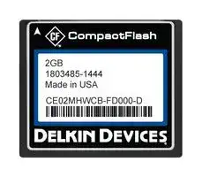
CE02MHWCB-FD000-D
MEMORY CARD, COMPACTFLASH, SLC, 2GB
⚠️ Reference pricing provided. In case of supply shortages, we will connect you with our trusted procurement partners to ensure your project's continuity.
- Manufacturer: DELKIN DEVICES
- Product type: Flash Memory Cards
- Product Range: C500 Series
- Memory Capacity: 2GB
- Blank Media Flash Memory Type: Compact Flash Card, Type I
| Delivery and price | |
|---|---|
| Units per pack | 20 |
| Price | 46.17 € |
| Current stock | 10+ |
| Lead time | 30 days |
Datasheet

Industrial UDMA 6 CompactFlash L500539 Rev. B

# **Industrial UDMA 6 CompactFlash**

# **Engineering Specification**

**Document Number L500539**

**Revision: B**

**CE64MGMCB-FD000-D**

No part of this document may be reproduced, copied, recorded, stored in a retrieval system, or transmitted in any form without the written permission of Delkin Devices. This document is for informational use only and is subject to change without prior notice. Delkin Devices assumes no responsibility for any errors that may appear in this document.

1

©2014 Delkin Devices, Inc.

Industrial UDMA 6 CompactFlash L500539 Rev. B

## **Table of Contents**

|1.0<br>Product Overview ............................................................................................................ 4|
|---|
|1.1<br>Part Numbers ........................................................................................................................................... 6|
|1.2<br>Mechanical Specifications ....................................................................................................................... 7|
|1.3<br>Dimensions .............................................................................................................................................. 7|
|2.0<br>Product Specifications .................................................................................................... 8|
|2.1<br>System Performance ............................................................................................................................... 8|
|2.2<br>Reliability ................................................................................................................................................. 8|
|2.3<br>Environmental Specifications .................................................................................................................. 8|
|3.0<br>CF Card Interface ........................................................................................................... 9|
|3.1<br>Card Pin Assignment ............................................................................................................................... 9|
|3.2<br>Card Pin Explanation ............................................................................................................................. 11|
|4.0<br>Electrical Interface ........................................................................................................ 16|
|4.1<br>Absolute Maximum Conditions .............................................................................................................. 16|
|4.2<br>Input Power ............................................................................................................................................ 16|
|4.3<br>Input Leakage Current ........................................................................................................................... 16|
|4.4<br>Input Characteristics .............................................................................................................................. 16|
|4.5<br>Output Drive Type .................................................................................................................................. 17|
|4.6<br>Output Drive Characteristics .................................................................................................................. 17|
|4.7<br>Interface/Bus Timing .............................................................................................................................. 17|
|4.8<br>CF-ATA Command Description ............................................................................................................. 17|
|4.8.1<br>CF-ATA Command set .................................................................................................................. 17|
|4.8.2<br>Check Power Mode – 98H or E5H ................................................................................................ 19|
|4.8.3<br>Execute Drive Diagnostics – 90H .................................................................................................. 20|
|4.8.4<br>Erase Sector(s) – C0H ................................................................................................................... 21|
|4.8.5<br>Flush Cache – E7h ........................................................................................................................ 21|
|4.8.6<br>Format Track – 50H ....................................................................................................................... 22|
|4.8.7<br>Identify Drive - ECH ....................................................................................................................... 22|
|5.0<br>Comparing CF-ATA to PC Card-ATA and True IDE ..................................................... 25|
|5.1<br>Electrical Differences ............................................................................................................................. 25|
|5.1.1<br>TTL Compatibility ........................................................................................................................... 25|
|5.1.2<br>Pull Up Resistor Input Leakage Current ........................................................................................ 25|
|5.2<br>Functional Differences ........................................................................................................................... 25|
|5.2.1<br>Additional Set Features Codes in CF-ATA .................................................................................... 25|
|5.2.2<br>Additional Commands in CF-ATA .................................................................................................. 25|
|5.2.3<br>Idle Timer ....................................................................................................................................... 25|
|5.2.4<br>Recovery from Sleep Mode ........................................................................................................... 26|
|6.0<br>SMART Functionality .................................................................................................... 27|
|6.1<br>SMART Data Structure .......................................................................................................................... 27|
|6.1.1<br>Spare Block Count Attribute .......................................................................................................... 28|
|6.1.2<br>Spare Block Count Worst Chip Attribute Threshold ...................................................................... 29|
|6.1.3<br>Erase Count Attribute .................................................................................................................... 29|


2

©2014 Delkin Devices, Inc.

Industrial UDMA 6 CompactFlash L500539 Rev. B

|6.1.4|Total ECC Errors Attribute ............................................................................................................. 30|
|---|---|
|6.1.5|Correctable ECC Errors Attribute .................................................................................................. 30|
|6.1.6|UDMA CRC Errors Attribute .......................................................................................................... 31|
|6.1.7|Total Number of Reads Attribute ................................................................................................... 31|
|6.1.8|Power On Count Attribute .............................................................................................................. 31|
|6.1.9|Total LBA’s Written Attribute.......................................................................................................... 32|
|6.1.10|Total LBA’s Read Attribute ............................................................................................................ 32|
|6.1.11|Anchor Block Status Attribute ........................................................................................................ 32|
|6.1.12|Trim Status Attribute ...................................................................................................................... 33|
|6.2<br>SMART Read Attribute Thresholds ....................................................................................................... 33||
|6.2.1|Spare Block Count Attribute Threshold ......................................................................................... 34|
|6.2.2|Spare Block Count Worst Chip Attribute Threshold ...................................................................... 34|
|6.2.3|Erase Count Attribute Threshold ................................................................................................... 34|
|6.2.4|Total ECC Errors Attribute Threshold ............................................................................................ 34|
|6.2.5|Correctable ECC Errors Attribute .................................................................................................. 34|
|6.2.6|UDMA CRC Errors Attribute .......................................................................................................... 34|
|6.2.7|Total Number of Reads Attribute ................................................................................................... 35|
|6.2.8|Power On Count Attribute .............................................................................................................. 35|
|6.2.9|Total LBAs Written Attribute .......................................................................................................... 35|
|6.2.10|Total LBAs Read Attribute ............................................................................................................. 35|
|6.2.11|Anchor Block Status Attribute ........................................................................................................ 35|
|6.2.12|Trim Status Attribute ...................................................................................................................... 35|
|6.3<br>SMART Return Status ........................................................................................................................... 36||
|6.4<br>SMART Read Log .................................................................................................................................. 36||
|6.5<br>SMART Write Log .................................................................................................................................. 37||
|6.6<br>SMART Read Remap Data ................................................................................................................... 38||
|6.7<br>SMART Read Wear Level Data ............................................................................................................. 38||


## **Table of Figures**

Figure 1. CF Card Dimensions ................................................................................................. 7

3

©2014 Delkin Devices, Inc.

Industrial UDMA 6 CompactFlash L500539 Rev. B

## **1.0 Product Overview**

Delkin’s Industrial UDMA 6 CompactFlash memory cards feature significant performance and robustness upgrades for industrial applications. These cards have superior features such as:

- Static and Global Wear Leveling

- BCH ECC error correction 6 or 8 bit / 512 Byte sector or 24 bit /1024 Byte double-sector with additional CRC

- Power loss detection and sudden power fail management

- Read disturb management

- Up to 60 MB/sec sustained write speed*

- °

- Industrial temperature (-40 to 85 C) operating range

- Compliant with CompactFlash Specification Rev. 4.1,  and compatible with 5.0 specifications, Type 1, and ATA/ATAPI-7

- Operating modes –  PIO 0 – 6, MDMA 0 – 6, UDMA 0 – 6 in True-IDE mode

- Compliant with European Union Directive 2002/95/EC (RoHS)

- Shock: 10g’s for 11ms, MIL-STD-810, Method 516.6

- Vibration: 20Hz to 2,000Hz, 7.7GRMS, MIL-STD-810, Method 514.6

- Humidity: 5 - 95% RH, non-condensing

- Altitude: 80,000 feet

- Capacities supported

   - SLC: 2GB - 64GB

- Supports 3.3-Volt and 5-Volt operation

- Fixed Drive and removable configurations available

- Solid State – no moving parts

- Ultrasonic welded case – No press fit components

- Available upon request – Custom CIS, mechanical features, programming, duplication, labels and packaging

- All capacity configurations are available with proprietary conformal coating

*Dependent on card capacity, host configuration and testing equipment.

4

©2014 Delkin Devices, Inc.

Industrial UDMA 6 CompactFlash L500539 Rev. B

The Industrial UDMA 6 CompactFlash cards are manufactured in the USA at our own facilities in Poway, California. The cards are supported by Delkin’s locked-down Bill of Materials that ensures consistent product performance and future compatibility. Delkin’s Industrial line of CompactFlash is the perfect solution for enterprises demanding specific higher qualitative and performance functions in a widely accepted, time-tested form factor.

## **Applications:**

- Industrial Computers

- Embedded Systems

- Data Acquisition

- Automotive

- Flight Systems ● Agriculture

- Manufacturing ● Gaming

- Military

- Telecommunications

## **Optional Conformal Coating**

Delkin’s proprietary conformal coating defends data integrity in harsh environments. Delkin utilizes a low-viscosity silicon elastomer that thoroughly covers exposed board and component surfaces with a protective coating. This process shields memory electronics from moisture and contamination, preventing metal corrosion and insulating conductors against electrical leakage. The coating also ruggedizes devices against the vibration, shock, and thermal stress of severe-service applications. Conformal coating is available as an option for Delkin industrial flash memory products in many form factors, including solid state drives, CompactFlash, Secure Digital, removable and embedded USB, PCMCIA, and mSATA.

5

©2014 Delkin Devices, Inc.

Industrial UDMA 6 CompactFlash L500539 Rev. B

## **1.1 Part Numbers**

Delkin Devices Industrial UDMA 6 CompactFlash cards are available in the following Configurations:

|Capacity *|Configuration|Part Number|
|---|---|---|
|2GB|SLC, Industrial Temp, Fixed Drive, DMA ON|CE02MHWCB-FD000-D|
||SLC, Industrial Temp, Fixed Drive, DMA OFF|CE02MHWCB-F1000-D|
||SLC, Industrial Temp, Removable, DMA ON|CE02MHWCB-XX000-D|
||SLC, Industrial Temp, Removable DMA, OFF|CE02MHWCB-X1000-D|
|4 GB|SLC, Industrial Temp, Fixed Drive, DMA ON|CE04TMCCB-FD000-D<br>CE04MHWCB-FD000-D|
||SLC, Industrial Temp, Fixed Drive, DMA OFF|CE04TMCCB-F1000-D<br>CE04MHWCB-F1000-D|
||SLC, Industrial Temp, Removable, DMA ON|CE04TMCCB-XX000-D<br>CE04MHWCB-XX000-D|
||SLC, Industrial Temp, Removable DMA, OFF|CE04TMCCB-X1000-D<br>CE04MHWCB-X1000-D|
|8 GB|SLC, Industrial Temp, Fixed Drive, DMA ON|CE08TLQCB-FD000-D|
||SLC, Industrial Temp, Fixed Drive, DMA OFF|CE08TLQCB-F1000-D|
||SLC, Industrial Temp, Removable, DMA ON|CE08TLQCB-XX000-D|
||SLC, Industrial Temp, Removable DMA, OFF|CE08TLQCB-X1000-D|
|16 GB|SLC, Industrial Temp, Fixed Drive, DMA ON|CE16TGPCB-FD000-D|
||SLC, Industrial Temp, Fixed Drive, DMA OFF|CE16TGPCB-F1000-D|
||SLC, Industrial Temp, Removable, DMA ON|CE16TGPCB-XX000-D|
||SLC, Industrial Temp, Removable DMA, OFF|CE16TGPCB-X1000-D|
|32 GB|SLC, Industrial Temp, Fixed Drive, DMA ON|CE32MGGCB-FD000-D|
||SLC, Industrial Temp, Fixed Drive, DMA OFF|CE32MGGCB-F1000-D|
||SLC, Industrial Temp, Removable, DMA ON|CE32MGGCB-XX000-D|
||SLC, Industrial Temp, Removable DMA, OFF|CE32MGGCB-X1000-D|
|64 GB|SLC, Industrial Temp, Fixed Drive, DMA ON|CE64MGMCB-FD000-D|
||SLC, Industrial Temp, Fixed Drive, DMA OFF|CE64MGMCB-F1000-D|
||SLC, Industrial Temp, Removable, DMA ON|CE64MGMCB-XX000-D|
||SLC, Industrial Temp, Removable DMA, OFF|CE64MGMCB-X1000-D|
|**Notes:**<br>To add optional Conformal Coating, change the000in the part number to0**5**0.<br>The CompactFlash cards are manufactured at our facilities in Poway, California USA.<br>Many custom configurations are available including custom CHS, mechanical features,<br>labels and packaging.<br>*Usable capacities are within 10% of the gross capacity figures shown above, which is<br>typical with all NAND flash devices, as a small portion of the total is needed for controller<br>firmware and spare block reserves.|||


6

©2014 Delkin Devices, Inc.

Industrial UDMA 6 CompactFlash L500539 Rev. B

## **1.2 Mechanical Specifications**

Delkin Devices Industrial UDMA 6 cards are Type I CompactFlash cards.

## **1.3 Dimensions**

|**1.3 Dimensions**||
|---|---|
|Length:|36.4 ± 0.15 mm (1.433 ±.006 in.)|
|Width:|42.80 ± 0.10 mm (1.685 ±.004 in.)|
|Thickness Including<br>Label Area:|3.3 mm ± 0.10 mm (.130 ± .004 in.)|
|Weight:|12.0 g typical|


**Figure 1. CF Card Dimensions**

7

©2014 Delkin Devices, Inc.

Industrial UDMA 6 CompactFlash L500539 Rev. B

## **2.0 Product Specifications**

## **2.1 System Performance**

|Parameter|Value|
|---|---|
|Data Transfer Rate|Upto 60 MB/s|
|Sustained Read|Upto 30 MB/s|
|Sustained Write|Upto 30 MB/s|


**Note** : All values dependent on configuration and testing environment.

## **2.2 Reliability**

|Parameter|Value|
|---|---|
|Endurance**|2GB:   195 TBW<br>4GB:   234 TBW<br>8GB:   468 TBW<br>16GB: 937 TBW<br>32GB: 1875 TBW<br>64GB:  3750 TBW|
|MTBF***|Up to 2,000,000 hours at 0`°`C|
|Data Retention|Flash dependent<br>2 – 16GB: 10 Years at up to 10% of P/E cycle rating,<br>1 Year at 100% of P/E cycles<br>32 – 64GB: 5 Years at up to 10% of P/E cycle rating,<br>1 Year at 100% of P/E cycles|
|Connector Durability|10,000 insertion cycles|


**Endurance estimates based on writing 8KB file size and calculated using a theoretical model. The figures provided are estimates and not guarantees of endurance. Actual results may vary depending on usage, operating temperature and other conditions. *** Dependent on configuration, testing environment and operating temperature.

## **2.3 Environmental Specifications**

|Features|Operating|
|---|---|
|Storage Temperature|-40 ~ 125°C|
|Industrial OperatingTemperature|-40 ~ 85°C|
|Humidity|5% – 95% RH, non-condensing|
|Vibration|20Hz to 2000Hz(MIL-STD-810, Method 514.5)|
|Shock|10g's for 11ms(MIL-STD-810, Method 516.6)|
|Altitude|80,000 feet max.|


8

©2014 Delkin Devices, Inc.

Industrial UDMA 6 CompactFlash L500539 Rev. B

## **3.0 CF Card Interface**

## **3.1 Card Pin Assignment**

||Memorycard mode|Memorycard mode|I/O card mode|I/O card mode|True IDE mode|True IDE mode|
|---|---|---|---|---|---|---|
|Pin No.|Signal Name|I/O|Signal Name|I/O|Signal Name|I/O|
|1|GND|—|GND|—|GND|—|
|2|D3|I/O|D3|I/O|D3|I/O|
|3|D4|I/O|D4|I/O|D4|I/O|
|4|D5|I/O|D5|I/O|D5|I/O|
|5|D6|I/O|D6|I/O|D6|I/O|
|6|D7|I/O|D7|I/O|D7|I/O|
|7|-CE1|I|-CE1|I|-CS0|I|
|8|A10|I|A10|I|A10|I|
|9|-OE|I|-OE|I|-ATASEL|I|
|10|A9|I|A9|I|A9|I|
|11|A8|I|A8|I|A8|I|
|12|A7|I|A7|I|A7|I|
|13|Vcc|—|Vcc|—|Vcc|—|
|14|A6|I|A6|I|A6|I|
|15|A5|I|A5|I|A5|I|
|16|A4|I|A4|I|A4|I|
|17|A3|I|A3|I|A3|I|
|18|A2|I|A2|I|A2|I|
|19|A1|I|A1|I|A1|I|
|20|A0|I|A0|I|A0|I|
|21|D0|I/O|D0|I/O|D0|I/O|
|22|D1|I/O|D1|I/O|D1|I/O|
|23|D2|I/O|D2|I/O|D2|I/O|
|24|WP|O|-IOIS16|O|-IOCS16|O|
|25|-CD2|O|-CD2|O|-CD2|O|
|26|-CD1|O|-CD1|O|-CD1|O|
|27|D11|I/O|D11|I/O|D11|I/O|
|28|D12|I/O|D12|I/O|D12|I/O|


9

©2014 Delkin Devices, Inc.

Industrial UDMA 6 CompactFlash L500539 Rev. B

||Memorycard mode|Memorycard mode|I/O card mode|I/O card mode|True IDE mode|True IDE mode|
|---|---|---|---|---|---|---|
|Pin No.|Signal Name|I/O|Signal Name|I/O|Signal Name|I/O|
|29|D13|I/O|D13|I/O|D13|I/O|
|30|D14|I/O|D14|I/O|D14|I/O|
|31|D15|I/O|D15|I/O|D15|I/O|
|32|-CE2|I|-CE2|I|-CS1|I|
|33|-VS1|O|-VS1|O|-VS1|O|
|34|-IORD|I|-IORD|I|-IORD|I|
|35|-IOWR|I|-IOWR|I|-IOWR|I|
|36|-WE|I|-WE|I|-WE|I|
|37|RDY/-BSY|O|-IREQ|O|INTRQ|O|
|38|Vcc|—|Vcc|—|Vcc|—|
|39|-CSEL|I|-CSEL|I|-CSEL|I|
|40|-VS2|O|-VS2|O|-VS2|O|
|41|RESET|I|RESET|I|-RESET|I|
|42|-WAIT|O|-WAIT|O|IORDY|O|
|43|-INPACK|O|-INPACK|O|DMARQ|O|
|44|-REG|I|-REG|I|-DMACK|I|
|45|BVD2|I/O|-SPKR|I/O|-DASP|I/O|
|46|BVD1|I/O|-STSCHG|I/O|-PDIAG|I/O|
|47|D8|I/O|D8|I/O|D8|I/O|
|48|D9|I/O|D9|I/O|D9|I/O|
|49|D10|I/O|D10|I/O|D10|I/O|
|50|GND|—|GND|—|GND|—|


10

©2014 Delkin Devices, Inc.

Industrial UDMA 6 CompactFlash L500539 Rev. B

## **3.2 Card Pin Explanation**

|Signal Name|Direction|Pin Number|Description|
|---|---|---|---|
|A10 to A0<br>(PC Card<br>Memorymode)|I|8, 10, 11,<br>12, 14,15,<br>16, 17, 18,<br>19, 20|Address bus is A10 to A0.  A10 is MSB and<br>A0 is LSB.|
|A10 to A0<br>(PC Card<br>Memorymode)||||
|A2 to A0<br>(True IDE mode)||18, 19, 20|Address bus is A10 to A0.  Only A2 to A0<br>are used, A10 to A3 should be grounded<br>bythe host.|
|BVD1<br>(PC Card<br>Memory mode)|I/O|46|BVD1 outputs the battery voltage status in<br>the card. This output line is constantly<br>driven to a high state since a battery is not<br>required for thisproduct.|
|-STSCHG<br>(PC Card I/O<br>mode)|||-STSCHG is used for changing the status<br>of Configuration and status register in<br>attribute area.|
|-PDIAG<br>(True IDE mode)|||-PDIAG is the Pass Diagnostic signal in<br>Master/Slave handshake protocol.|
|BVD2<br>(PC Card<br>Memory mode)|I/O|45|BVD2 outputs the battery voltage status in<br>the card. This output line is constantly<br>driven to a high state since a battery is not<br>required for thisproduct.|
|-SPKR<br>(PC Card I/O<br>mode)|||-SPKR outputs speaker signals.  This<br>output line is constantly driven to a high<br>state since this product does not support<br>the audio function.|
|-DASP<br>(True IDE mode)|||-DASP is the Disk Active/Slave Present<br>signal in the Master/Slave handshake<br>protocol.|
|-CD1, -CD2<br>(PC Card<br>Memory mode)|O|26, 25|-CD1 and -CD2 are the card detection<br>signals. -CD1 and -CD2 are connected to<br>ground, so host can detect that the card is<br>inserted or not.|
|-CD1, -CD2<br>(PC Card I/O<br>mode)||||
|-CD1, -CD2<br>(True IDE mode)||||


11

©2014 Delkin Devices, Inc.

Industrial UDMA 6 CompactFlash L500539 Rev. B

|Signal Name|Direction|Pin Number|Description|
|---|---|---|---|
|-CE1, -CE2<br>PC Card Memory<br>mode)<br>Card Enable|I|7, 32|-CE1 and -CE2 are low active card select<br>signals. Byte/Word/Odd byte modes are<br>defined by combination Card Enable of -<br>CE1, -CE2 and A0.|
|-CE1, -CE2<br>(PC Card I/O<br>mode)<br>Card Enable||||
|-CS0, -CS1<br>(True IDE mode)<br>Card Enable|||-CE2 is used for select the Alternate Status<br>Register and the Device Control Register<br>while -CE1 is the chip select for the other<br>task file registers.|
|-CSEL<br>(PC Card Memory<br>mode)|I|39|This signal is not used.|
|-CSEL<br>(PC Card I/O mode)||||
|-CSEL<br>(True IDE mode)|||This signal is used to configure this device<br>as a<br>Master or a Slave when configured in the<br>True IDE mode. When this pin is grounded,<br>this device is configured as a Master.<br>When the pin is open, this device is<br>configured as a Slave.|
|D15 to D0<br>(PC Card Memory<br>mode)|I/O|31, 30, 29,<br>28, 27, 49,<br>48, 47, 6, 5,<br>4, 3, 2, 23,<br>22, 21|Data bus is D15 to D0. D0 is the LSB of the<br>even byte of the word. D8 is the LSB of the<br>odd byte of the word.|
|D15 to D0<br>(PC Card I/O mode)||||
|D15 to D0<br>(True IDE mode)||||
|GND<br>(PC Card Memory<br>mode)|—|1, 50|Ground|
|GND<br>(PC Card I/O mode)||||
|GND<br>(True IDE mode)||||
|-INPACK<br>(PC Card Memory<br>mode)|O|43|This signal is not used and should not be<br>connected at the host.|


12

©2014 Delkin Devices, Inc.

Industrial UDMA 6 CompactFlash L500539 Rev. B

|Signal Name|Direction|Pin Number|Description|
|---|---|---|---|
|-INPACK<br>(PC Card I/O mode)<br>Input Acknowledge|||This signal is asserted low by this card<br>when the card is selected and responding<br>to an I/O read cycle at the address that is<br>on the address bus during -CE and-IORD<br>are low. This signal is used for the input<br>data buffer control.|
|DMARQ<br>(True IDE mode)|||This signal is a DMA Request that is used<br>for DMA data transfers between host and<br>device.|
|-IORD<br>(PC Card Memory<br>mode)|I|34|This signal is not used.|
|-IORD<br>(PC Card I/O mode)|||-IORD is used for control of read data in<br>I/O task file area. This card does not<br>respond to -IORD until I/O card interface<br>settingup.|
|-IORD<br>(True IDE mode)|||-IORD is used for control of read data in<br>I/O task file area. This card does not<br>respond to -IORD until True IDE interface<br>settingup.|
|-IOWR<br>(PC Card Memory<br>mode)|I|35|This signal is not used.|
|-IOWR<br>(PC Card I/O mode)|||-IOWR is used for control of data write in<br>I/O task file area. This card does not<br>respond to -IOWR until I/O card interface<br>settingup.|
|-IOWR<br>(True IDE mode)|||-IOWR is used for control of data write in<br>I/O task file area. This card does not<br>respond to -IOWR until True IDE interface<br>settingup.|
|-OE<br>(PC Card Memory<br>mode)|I|9|-OE is used for the control of reading<br>register’s data in attribute area or task file<br>area.|
|-OE<br>(PC Card I/O mode)|||-OE is used for the control of reading<br>register’s data in attribute area.|
|-ATASEL<br>(True IDE mode)|||To enable True IDE mode this input should<br>be grounded by the host.|
|RDY/-BSY<br>(PC Card Memory<br>mode)|O|37|The signal is RDY/-BSY pin. RDY/-BSY pin<br>turns low level during the card internal<br>initialization operation at Vcc applied or<br>reset applied, so next access to the card<br>should be after the signal turned high level.|


13

©2014 Delkin Devices, Inc.

Industrial UDMA 6 CompactFlash L500539 Rev. B

|Signal Name|Direction|Pin Number|Description|
|---|---|---|---|
|-IREQ<br>(PC Card I/O mode)|||This signal is active low -IREQ pin.  The<br>signal of low level indicates that the card is<br>requesting software service to host, and<br>high level indicates that the card is not<br>requesting.|
|INTRQ<br>(True IDE mode)|||This signal is the active high Interrupt<br>Request to the host.|
|-REG<br>(PC Card Memory<br>mode)|I|44|-REG is used during memory cycles to<br>distinguish between task file and attribute<br>memory accesses. Attribute memory select<br>High for task file, Low for attribute memory<br>is accessed.|
|-REG<br>(PC Card I/O mode)|||-REG is constantly low when task file or<br>attribute memory is accessed.|
|-DMACK<br>(True IDE mode)|||This is a DMA Acknowledge signal by the<br>host in response to DMARQ to initiate DMA<br>transfers.|
|RESET<br>(PC Card Memory<br>mode)|I|41|This signal is active high RESET pin.  If<br>this signal is asserted high, the card<br>internal initialization begins to operate.<br>During the card internal initialization RDY/-<br>BSY is low.  After the card internal<br>initialization RDY/-BSY is high.|
|RESET<br>(PC Card I/O mode)|||This signal is active high RESET pin.  If<br>this signal is asserted high, the card<br>internal initialization begins to operate.  In<br>this mode, RDY/-BSY signal cannot be<br>used, so using Status Register the<br>Ready/Busystatus can be confirmed.|
|-RESET<br>(True IDE mode)|||This signal is active low -RESET pin.  If this<br>signal is asserted low, all the registers in<br>this card are reset. In this mode, RDY/-<br>BSY signal cannot be used, so using status<br>register the Ready/Busy status can be<br>confirmed.|
|Vcc<br>(PC Card Memory<br>mode)|—|13, 38|+5 V, +3.3 V power.|
|Vcc<br>(PC Card I/O mode)||||
|Vcc<br>(True IDE mode)||||


14

©2014 Delkin Devices, Inc.

Industrial UDMA 6 CompactFlash L500539 Rev. B

|Signal Name|Direction|Pin Number|Description|
|---|---|---|---|
|-VS1, -VS2<br>(PC Card Memory<br>mode)|O|33, 40|These signals are intended to notify Vcc<br>requirement to host.  -VS1 is held<br>grounded and -VS2 is non-connected in<br>this card.|
|-VS1, -VS2<br>(PC Card I/O mode)||||
|-VS1, -VS2<br>(True IDE mode)||||
|-WAIT<br>(PC Card Memory<br>mode)|O|42|This signal is active low -WAIT pin.  In this<br>card this signal is constantly high level.|
|-WAIT<br>(PC Card I/O mode)||||
|IORDY<br>(True IDE mode)|||This output signal may be used as IORDY.<br>In this card this signal is constantly high<br>impedance.|
|-WE<br>(PC Card Memory<br>mode)|I|36|-WE is used for the control of writing<br>register’s data in attribute memory area or<br>task file area.|
|-WE<br>(PC Card I/O mode)|||-WE is used for the control of writing<br>register’s data in attribute memory area.|
|-WE<br>(True IDE mode)|||This input signal is not used and should be<br>connected to Vcc by the host.|
|WP<br>(PC Card Memory<br>mode)|O|24|WP is held low because this card does not<br>have write-protect switch.|
|-IOIS16<br>(PC Card I/O mode)|||-IOIS16 is asserted when task file registers<br>are accessed in 16-bit mode.|
|-IOCS16<br>(True IDE mode)|||This output signal is asserted low when this<br>device is expecting a word data transfer<br>cycle.|


15

©2014 Delkin Devices, Inc.

Industrial UDMA 6 CompactFlash L500539 Rev. B

## **4.0 Electrical Interface**

## **4.1 Absolute Maximum Conditions**

|Parameter|Symbol|Conditions|
|---|---|---|
|Input Power|Vcc|-0.3V min. to 6.7V Max|
|Voltage on any pin except Vcc with<br>respect to GND|V|-0.3V min. to Vcc + 0.3V Max|


## **4.2 Input Power**

|Voltage|Maximum Average<br>RMS Active Current|Maximum Average<br>RMS SleepCurrent|Measurement<br>Method|
|---|---|---|---|
|3.135-3.465V|110 mA|3 mA|3.3V at 25ºC¹|
|4.5-5.5V|75 mA|3 mA|5.0V at 25ºC¹|


## **4.3 Input Leakage Current**

|Type|Parameter|Symbol|Conditions|Min|Typ|Max|Units|
|---|---|---|---|---|---|---|---|
|IxZ|Input Leakage<br>Current|IL|VHI = Vcc / VIL =<br>GND|-1||1|µA|
|IxU|Pull UpResistor|RPU1|Vcc = 5.0V|50k||500k|Ohm|
|IxD|Pull Down Resister|RPD1|Vcc = 5.0V|50k||500k|Ohm|


## **4.4 Input Characteristics**

|Type|Parameter|Symbo<br>l|Min           Typ<br>Max|Min           Typ<br>Max|Min           Typ<br>Max|<br>Min           Typ<br>Max|<br>Min           Typ<br>Max|<br>Min           Typ<br>Max|<br>Units|
|---|---|---|---|---|---|---|---|---|---|
||||Vcc = 3.3V|||Vcc = 5.0V||||
|1|Input Voltage<br>CMOS|Vih<br>Vil|2.4||0.6|4.0||0.8|Volts|
|2|Input Voltage<br>CMOS|Vih<br>Vil|1.5||0.6|2.0||0.8|Volts|
|3|Input Voltage<br>CMOS Schmitt<br>Trigger|Vth<br>Vtl||1.8<br>1.0|||2.8<br>2.0||Volts|


16

©2014 Delkin Devices, Inc.

Industrial UDMA 6 CompactFlash L500539 Rev. B

## **4.5 Output Drive Type**

All outputs drive types are CMOS level.

## **4.6 Output Drive Characteristics**

|Type|Parameter|Symbol|Conditions|Min|Typ|Max|Units|
|---|---|---|---|---|---|---|---|
|O1|Output<br>Voltage|Voh<br>Vol|Ioh = -4<br>mA<br>Iol = 4 mA|Vcc -0.8V||GND<br>+0.4V|Volts|
|02|Output<br>Voltage|Voh<br>Vol|Ioh = -8<br>mA<br>Iol = 8 mA|Vcc -0.8V||GND<br>+0.4V|Volts|


## **4.7 Interface/Bus Timing**

There are two types of bus cycles and timing sequences that occur in the PCMCIA type interface, a direct mapped I/O transfer and a memory access. The two timing sequences are explained in detail in the PCMICA PC Card Standard. Delkin’s CompactFlash Card conforms to the timing in that reference document.

## **4.8 CF-ATA Command Description**

This section defines the software requirements and the format of the commands the host sends to the CompactFlash cards. Commands are issued to the CompactFlash card by loading the required registers in the command block with the supplied parameters, and then writing the command code to the Command register. The manner in which a command is accepted varies. These are three classes of command acceptance, all dependent on the host not issuing commands unless the CompactFlash card is not busy (BSY=0).

## **4.8.1 CF-ATA Command set**

The following table summarizes the CF-ATA command set with the paragraphs that follow describing the individual commands and the tasks file for each.

Class COMMAND Code FR SC SN CY DH LBA

17

©2014 Delkin Devices, Inc.

Industrial UDMA 6 CompactFlash

L500539 Rev. B

|Class|<br>COMMAND|Code|FR|SC|SN|CY|DH|LBA|
|---|---|---|---|---|---|---|---|---|
|1|Check Power Mode|E5h or 98h|-|-|-|-|D|-|
|1|Execute Drive Diagnostic|90h|-|-|-|-|D|-|
|1|Erase Sector(s)|C0h|-|Y|Y|Y|Y|Y|
|1|Flush Cache|E7h|-|-|-|-|D|-|
|2|Format Track|50h|-|Y|-|Y|Y|Y|
|1|Identify Device|ECh|-|-|-|-|D|-|
|1|Idle|E3h or 97h|-|Y|-|-|D|-|
|1|Idle Immediate|E1h or 95h|-|-|-|-|D|-|
|1|Initialize Drive Parameters|91h|-|Y|-|-|Y|-|
|1|Key Management Structure Read|B9 Feature 0-127|C|C|C|C|D C|-|
|1|Key Management Read Keying<br>Material|B9 Feature 80|C|C|C|C|D C|-|
|2|Key Management Change Key<br>Management Value|B9 Feature 81|C|C|C|C|D C|-|
|1|NOP|00h|-|-|-|-|D|-|
|1|Read Buffer|E4h|-|-|-|-|D|-|
|1|Read DMA|C8h|-|Y|Y|Y|Y|Y|
|1|Read Long Sector|22h or 23h|-|-|Y|Y|Y|Y|
|1|Read Multiple|C4h|-|Y|Y|Y|Y|Y|
|1|Read Sector(s)|20h or 21h|-|Y|Y|Y|Y|Y|
|1|Read Verify Sector(s)|40h or 41h|-|Y|Y|Y|Y|Y|
|1|Recalibrate|1Xh|-|-|-|-|D|-|
|1|Request Sense|03h|-|-|-|-|D|-|
|1|Security Disable Password|F6h|-|-|-|-|D|-|
|1|Security Erase Prepare|F3h|-|-|-|-|D|-|
|1|Security Erase Unit|F4h|-|-|-|-|D|-|
|1|Security Freeze Lock|F5h|-|-|-|-|D|-|
|1|Security Set Password|F1h|-|-|-|-|D|-|
|1|Security Unlock|F2h|-|-|-|-|D|-|
|1|Seek|7Xh|-|-|Y|Y|Y|Y|
|1|Set Features|EFh|Y|-|-|-|D|-|
|1|Set Multiple Mode|C6h|-|Y|-|-|D|-|
|1|Set Sleep Mode|E6h or 99h|-|-|-|-|D|-|
|1|Standby|E2h or 96h|-|-|-|-|D|-|
|1|Standby Immediate|E0h or 94h|-|-|-|-|D|-|
|1|Translate Sector|87h|-|Y|Y|Y|Y|Y|


18

©2014 Delkin Devices, Inc.

Industrial UDMA 6 CompactFlash L500539 Rev. B

|Class|<br>COMMAND|Code|FR|SC|SN|CY|DH|LBA|
|---|---|---|---|---|---|---|---|---|
|1|Wear Level|F5h|-|-|-|-|Y|-|
|2|Write Buffer|E8h|-|-|-|-|D|-|
|2|Write DMA|CAh|-|Y|Y|Y|Y|Y|
|2|Write Long Sector|32h or 33h|-|-|Y|Y|Y|Y|
|3|Write Multiple|C5h|-|Y|Y|Y|Y|Y|
|3|Write Multiple w/o Erase|CDh|-|Y|Y|Y|Y|Y|
|2|Write Sector(s)|30h or 31h|-|Y|Y|Y|Y|Y|
|2|Write Sector(s) w/o Erase|38h|-|Y|Y|Y|Y|Y|
|3|Write Verify|3Ch|-|Y|Y|Y|Y|Y|


1. FR = Features Register

2. SC = Sector Count Register

3. SN = Sector Number Register

4. CY = Cylinder Register

5. DH = Card/Drive/Head Register

6. LBA = Logical Block Address Mode Supported (see command description for use).

7. Y = The register contains a valid parameter for this command.

8. For the Drive/Head Register:

   - Y – both the CompactFlash card and head parameters are used;

   - D – only the CompactFlash card parameter is valid and not the head parameter.

## **4.8.2 Check Power Mode – 98H or E5H**

|**Bit –>**|**7**|**6**|**5**|**4**|**3**|**2**|**1**|**0**|
|---|---|---|---|---|---|---|---|---|
|**Command (7)**|98h or E5h||||||||
|**C/D/H (6)**|X|||Drive|X||||
|**Cyl High (5)**|X||||||||
|**Cyl Low (4)**|X||||||||
|**Sec Num (3)**|X||||||||
|**Sec Cnt (2)**|X||||||||
|**Feature (1)**|X||||||||


- This command checks the power mode.

- Because Delkin’s CompactFlash card can recover from sleep in 200ms, idle mode is never enabled.

- CompactFlash card sets BSY, sets the Sector Count Register to 00H, Clears BSY and generates an interrupt.

19

©2014 Delkin Devices, Inc.

Industrial UDMA 6 CompactFlash L500539 Rev. B

## **4.8.3 Execute Drive Diagnostics – 90H**

|**Bit –>**|**7**|**6**|**5**|**4**|**3**|**2**|**1**|**0**|
|---|---|---|---|---|---|---|---|---|
|**Command**<br>**(7)**|90H||||||||
|**C/D/H (6)**|X|||Drive|X||||
|**Cyl High (5)**|X||||||||
|**Cyl Low (4)**|X||||||||
|**Sec Num (3)**|X||||||||
|**Sec Cnt (2)**|X||||||||
|**Feature (1)**|X||||||||


This command performs the internal diagnostic test implemented by the CompactFlash card.

If in PCMCIA configuration this command runs only on the CompactFlash card which is addressed by the Drive/Head register when the diagnostic command is issued. This is because PCMCIA card interface does not allow for direct inter-drive communication (such as the ATA PDIAG and DASP signals). If in True IDE mode the Drive bit is ignored and the diagnostic command is executed by both the master and the slave with the master responding with status for both devices.

The Diagnostic codes shown below are returned in the Error register at the end of the command.

## **Diagnostic Codes**

|Code|Error Type|
|---|---|
|01H|No Error Detected|
|02H|Formatter Device Error|
|03H|Sector Buffer Error|
|04H|ECC Circuitry Error|
|05H|Controlling Microprocessor Error|
|8XH|Slave Error in True IDE mode|


20

©2014 Delkin Devices, Inc.

Industrial UDMA 6 CompactFlash L500539 Rev. B

## **4.8.4 Erase Sector(s) – C0H**

|**Bit –>**|**7**|**6**|**5**|**4**|**3**|**2**|**1**|**0**|
|---|---|---|---|---|---|---|---|---|
|**Command (7)**|C0H||||||||
|**C/D/H (6)**|1|LBA|1|Drive|Head (LBA 27-24)||||
|**Cyl High (5)**|Cylinder High (LBA 23-16)||||||||
|**Cyl Low (4)**|Cylinder Low (LBA 15-8)||||||||
|**Sec Num (3)**|Sector Number (LBA 7-0)||||||||
|**Sec Cnt (2)**|Sector Count||||||||
|**Feature (1)**|X||||||||


This command is used to pre-erase and condition data sectors in advance of a Write without Erase or Write Multiple without Erase command. There is no data transfer associated with this command but a Write Fault error status can occur.

## **4.8.5 Flush Cache – E7h**

|**Flush Cache –**|**E7h**||||||||
|---|---|---|---|---|---|---|---|---|
|**Bit ->**|**7**|**6**|**5**|**4**|**3**|**2**|**1**|**0**|
|**Command (7)**|E7h||||||||
|**C/D/H (6)**|X|||Drive|X||||
|**Cyl High (5)**|X||||||||
|**Cyl Low (4)**|X||||||||
|**Sec Num (3)**|X||||||||
|**Sec Cnt (2)**|X||||||||
|**Feature (1)**|X||||||||


This command causes the card to complete writing data from its cache. The card returns status with RDY=1 and DSC=1 after the data in the write cache buffer is written to the media. If the Compact Flash Card does not support the Flush Cache command, the Compact Flash Card shall return command aborted.

21

©2014 Delkin Devices, Inc.

Industrial UDMA 6 CompactFlash L500539 Rev. B

## **4.8.6 Format Track – 50H**

|**Bit –>**|**7**|**6**|**5**|**4**|**3**|**2**|**1**|**0**|
|---|---|---|---|---|---|---|---|---|
|**Command (7)**|50H||||||||
|**C/D/H (6)**|1|LBA|1|Drive|Head (LBA 27-24)||||
|**Cyl High (5)**|Cylinder High (LBA 23-16)||||||||
|**Cyl Low (4)**|Cylinder Low (LBA 15-8)||||||||
|**Sec Num (3)**|X (LBA 7-0)||||||||
|**Sec Cnt (2)**|Count (LBA mode only)||||||||
|**Feature (1)**|X||||||||


This command writes the desired head and cylinder of the selected drive with a vendor unique data pattern (typically FFH or 00H). To remain host backward compatible, the CompactFlash card expects a sector buffer of data from the host to follow the command with the same protocol as the Write Sector(s) command although the information in the buffer is not used by the CompactFlash card. If LBA=1 then the number of sectors to format is taken from Sec Cnt register (0=256). The use of this command is not recommended.

## **4.8.7 Identify Drive - ECH**

|**Bit –>**|**7**|**6**|**5**|**4**|**3**|**2**|**1**|**0**|
|---|---|---|---|---|---|---|---|---|
|**Command (7)**|ECH||||||||
|**C/D/H (6)**|X|X|X|Drive|X||||
|**Cyl High (5)**|X||||||||
|**Cyl Low (4)**|X||||||||
|**Sec Num (3)**|X||||||||
|**Sec Cnt (2)**|X||||||||
|**Feature (1)**|X||||||||


The Identify Drive command enables the host to receive parameter information from the CompactFlash card. This command has the same protocol as the Read Sector(s) command.

22

©2014 Delkin Devices, Inc.

Industrial UDMA 6 CompactFlash L500539 Rev. B

## **Identify Drive Information**

|Word<br>Address|<br>Default<br>Value|Total<br>Bytes|<br>Data Field Type Information|
|---|---|---|---|
|0|848Ah|<br>2|<br>General configuration - signature for the CompactFlash Card|
||0XXX|2|General configuration – Bit Significant with ATA-4 definitions|
|1|XXXXh|2|Default number of cylinders|
|2|0000h|2|Reserved|
|3|00XXh|2|Default number of heads|
|4|0000h|2|Obsolete|
|5|0000h|2|Obsolete|
|6|XXXXh|2|Default number of sectors per track|
|7-8|XXXXh|4|Number of sectors per card (Word 7=MSW, Word 8=LSW)|
|9|XXXXh|2|Obsolete|
|10-19|aaaa|20|Serial number in ASCII (Right Justified)|
|20|0000h|2|Obsolete|
|21|0000h|2|Obsolete|
|22|0004h|2|Number of ECC bytes passed on Read/Write Long Commands|
|23-26|aaaa|8|Firmware revision in ASCII. Big Endian Byte Order in Word|
|27-46|aaaa|40|Model number in ASCII (Left Justified) Big Endian Byte Order in Word|
|47|XXXXh|2|Maximum number of sectors on Read/Write Multiple command|
|48|0000h|2|Reserved|
|49|XX00h|2|Capabilities|
|50|0000h|2|Reserved|
|51|0X00h|2|PIO data transfer cycle timing mode|
|52|0000h|2|Obsolete|
|53|000Xh|2|Field Validity|
|54|XXXXh|2|Current numbers of cylinders|
|55|XXXXh|2|Current numbers of heads|
|56|XXXXh|2|Current sectors per track|
|57-58|XXXXh|4|Current capacity in sectors (LBAs)(Word 57=LSW, Word 58=MSW)|
|59|01XXh|2|Multiple sector setting|
|60-61|XXXXh|4|Total number of sectors addressable in LBA Mode|
|62|0000h|2|Reserved|
|63|0X0Xh|2|Multiword DMA transfer. In PCMCIA mode this value shall be 0h|
|64|00XXh|2|Advanced PIO modes supported|
|65|XXXXh|2|Minimum Multiword DMA transfer cycle time per word. In PCMCIA mode<br>this value shall be 0h|


23

©2014 Delkin Devices, Inc.

Industrial UDMA 6 CompactFlash L500539 Rev. B

|Word<br>Address|<br>Default<br>Value|Total<br>Bytes|<br>Data Field Type Information|
|---|---|---|---|
|66|XXXXh|<br>2|<br>Recommended Multiword DMA transfer cycle time. In PCMCIA mode this<br>value shall be 0h|
|67|XXXXh|2|Minimum PIO transfer cycle time without flow control|
|68|XXXXh|2|Minimum PIO transfer cycle time with IORDY flow control|
|69-127|0000h|116|Reserved|
|128|XXXXh|2|Security status|
|129-159|<br>0000h|64|Vendor unique bytes|
|160-255|<br>0000h|172|Reserved|


24

©2014 Delkin Devices, Inc.

Industrial UDMA 6 CompactFlash L500539 Rev. B

## **5.0 Comparing CF-ATA to PC Card-ATA and True IDE**

This section details the differences between CF-ATA when compared to the _PC Card-ATA_ and _True IDE_ .

## **5.1 Electrical Differences**

## **5.1.1 TTL Compatibility**

CF is not TTL compatible, it is a purely CMOS interface. Refer to Electrical Specification section covered earlier in this document.

## **5.1.2 Pull Up Resistor Input Leakage Current**

The minimum pull up input leakage current is 50K ohms rather than the 10K ohms stated in the PCMCIA specification.

## **5.2 Functional Differences**

## **5.2.1 Additional Set Features Codes in CF-ATA**

The following _Set Features_ codes provide additional functionality in CF-ATA, but are not standard in PC Card-ATA or True IDE:

1. 69H, Accepted for backward compatibility

2. 96H, Accepted for backward compatibility

3. 97H, Accepted for backward compatibility

4. 9AH, Set the host current source capability

## **5.2.2 Additional Commands in CF-ATA**

The following commands provide additional functionality in CF-ATA, but are not standard PC Card-ATA commands.

PC Card-ATA and True IDE define the following command codes as _vendor unique_ :

1. C0H, Erase Sectors

2. 87H, Translate Sector

3. F5H, Wear Level

PC Card-ATA and True IDE define the following command codes as _reserved_ :

1. 03H, Request Sense

2. 38H, Write Without Erase

3. CDH, Write Multiple Without Erase

## **5.2.3 Idle Timer**

The CF-ATA Idle timer uses an increment value of 5 ms, rather than the 5 second minimum increment value specified in PC Card-ATA/True IDE.

25

©2014 Delkin Devices, Inc.

Industrial UDMA 6 CompactFlash

L500539 Rev. B

## **5.2.4 Recovery from Sleep Mode**

For CF devices, recovery from sleep mode is accomplished by issuing another command to the device. A hardware or software reset is not required.

26

©2014 Delkin Devices, Inc.

Industrial UDMA 6 CompactFlash L500539 Rev. B

## **6.0 SMART Functionality**

Delkin Devices Industrial UDMA 6 CF cards support the following SMART commands, determined by the Feature Register value.

|Value|Command|
|---|---|
|D0h|SMART Read Data|
|D1h|SMART Read Attribute Thresholds|
|D2h|SMART Enable / Disable Attribute Autosave|
|D5h|SMART Read Log|
|D6h|SMART Write Log|
|D8h|SMART Enable Operations|
|D9h|SMART Disable Operations|
|DAh|Return Status|
|E0h|SMART Read Remap Data|
|E1h|SMART Read Wear Level Data|


SMART commands with Feature Register values not mentioned in the above table are not supported and will be aborted.

## **6.1 SMART Data Structure**

The following 512 bytes make up the device SMART data structure. Users can obtain the data using the “Read Data” command (D0h.)

|Byte|Value|Description|
|---|---|---|
|0 – 1|0010h|SMART structure version|
|2 – 361||Attribute entries 1 to 30 (12 bytes each)|
|362|00h|Off-line data collection status  (no off-line data collection)|
|363|00h|Self-test execution status byte (self-test completed)|
|364 – 365|0000h|Total time in seconds to complete off-line data collection activity|
|366|00h|Vendor specific|
|367|00h|Off-line data collection capability (no off-line data collection)|
|368 – 369|0003h|SMART capability|
|370|00h|Error logging capability (no error logging)|
|371|00h|Vendor specific|


27

©2014 Delkin Devices, Inc.

Industrial UDMA 6 CompactFlash L500539 Rev. B

|372|00h|Short self-test routine recommended polling time (in minutes)|
|---|---|---|
|373|00h|Extended self-test routine recommended polling time (in<br>minutes)|
|374 – 385|00h|Reserved|
|386 – 387|0004h|SMART Structure Version|
|388 – 391||Firmware “Commit” Counter|
|392 - 395||Firmware Wear Level Threshold|
|396||Global Wear Leveling Active|
|397||Global Bad Block Management active<br>(returns 0 if bad block management is still at local chip level, and returns 1 if global<br>bad block management has begun.)|
|398 – 401||Average Flash Block Erase Count|
|402 – 405||Number of Flash Blocks involved in the Wear Leveling|
|406 – 409||Number of total ECC errors during firmware initialization|
|410 – 413||Number of correctable ECC errors during firmware initialization|
|414 – 510|00h|Vendor specific|
|511||Data structure checksum|


## **6.1.1 Spare Block Count Attribute**

This attribute gives information about the amount of available spare blocks.

|Offset|Value|Description<br>Attribute ID – Reallocation Count<br>Flags – Pre-fail type, attribute value is updated during normal<br>operation<br>Attribute value.  The value returned here is the percentage of<br>remaining spare blocks summed over all flash chips, i.e.<br>(100 x current spare blocks / initial spare blocks)<br>Attribute value (worst value)<br>Sum of the initial number of spare blocks for all flash chips<br>Sum of the current number of spare blocks for all flash chips<br>Reserved|
|---|---|---|
|0|196||
|1 – 2|0003h||
|3|||
|4|||
|5 – 7|||
|8 – 10|||
|11|00h||


This attribute is used for the SMART Return Status command.  If the attribute value field is less than the spare block threshold (set with the –tsbc preformat option), the SMART Return Status command will indicate a threshold exceeded condition.

28

©2014 Delkin Devices, Inc.

Industrial UDMA 6 CompactFlash L500539 Rev. B

## **6.1.2 Spare Block Count Worst Chip Attribute Threshold**

This attribute gives information about the amount of available spare blocks on the flash chip that has the lowest current number of spare blocks.

|Offset|Value|Description|
|---|---|---|
|0|213|Attribute ID – Spare Block Count Worst Chip (vendor specific)|
|1 – 2|0002h|Flags – Advisory type, attribute value is updated during normal<br>operation|
|3|64h|Attribute value.  This value is fixed at 100.|
|4|64h|Attribute value (worst value)|
|5 – 7||Initial number of spare blocks for the flash chip with the lowest current<br>number of spare blocks.|
|8 – 10||Current number of spare blocks for the flash chip with the lowest<br>current number of spare blocks.|
|11|00h|Reserved|


## **6.1.3 Erase Count Attribute**

This attribute gives information about the amount of flash block erases that have been performed.

|Offset|Value|Description|
|---|---|---|
|0|229|Attribute ID – Erase Count Usage (vendor specific)|
|1 – 2|000Xh|Flags – Pre-fail or Advisory type, attribute value is updated during<br>normal operation|
|3||Attribute value.  The value returned here is an estimation of the<br>remaining card life, in percent, based on the number of flash block<br>erases compared to the target number of erase cycles per block.|
|4||Attribute value (worst value)|
|5 - 10||Estimated total number of block erases.|
|11|00h|Reserved|


This attribute is used for the SMART Return Status command.  If the attribute value field is less than the erase count threshold (set with the –tec preformat option), the SMART Return Status command will indicate a threshold exceeded condition.

The target number of erase cycles per flash block is taken from the –mbec preformat option, or if this option is absent, from the MaxBlockEraseCount column in the Device Description file.

The attribute type (pre-fail or advisory) can be set with the –ecwl preformat option.

29

©2014 Delkin Devices, Inc.

Industrial UDMA 6 CompactFlash L500539 Rev. B

## **6.1.4 Total ECC Errors Attribute**

This attribute gives information about the total number of ECC errors that have occurred on flash read commands during firmware runtime.  This attribute is not used for the SMART Return Status command.

|Offset|Value|Description|
|---|---|---|
|0|203|Attribute ID – Number of ECC Errors|
|1 – 2|0002h|Flags – Advisory type, attribute value is updated during normal operation|
|3|64h|Attribute value.  This value is fixed at 100.|
|4|64h|Attribute value (worst value)|
|5 – 8||Total number of ECC errors (correctable and uncorrectable)|
|9 – 10||---|
|11|00h|Reserved|


## **6.1.5 Correctable ECC Errors Attribute**

This attribute gives information about the total number of correctable ECC errors that have occurred on flash read commands during firmware runtime.  This attribute is not used for the SMART Return Status command.

|Offset|Value|Description|
|---|---|---|
|0|204|Attribute ID – Number of corrected ECC Errors|
|1 – 2|0002h|Flags – Advisory type, attribute value is updated during normal operation|
|3|64h|Attribute value.  This value is fixed at 100.|
|4|64h|Attribute value (worst value)|
|5 – 8||Total number of correctable ECC errors|
|9 - 10||---|
|11|00h|Reserved|


30

©2014 Delkin Devices, Inc.

Industrial UDMA 6 CompactFlash L500539 Rev. B

## **6.1.6 UDMA CRC Errors Attribute**

This attribute gives information about the total number of UDMA CRC errors that have occurred on flash read commands.  This attribute is not used for the SMART Return Status command.

|Offset|Value|Description|
|---|---|---|
|0|199|Attribute ID – UDMA CRC error rate|
|1 – 2|0002h|Flags – Advisory type, attribute value is updated during normal operation|
|3|64h|Attribute value.  This value is fixed at 100.|
|4|64h|Attribute value (worst value)|
|5 – 8||Total number of UDMA CRC errors|
|9 – 10||---|
|11|00h|Reserved|


## **6.1.7 Total Number of Reads Attribute**

This attribute gives information about the total number of flash read commands. This can be useful for interpretation of the number of correctable or total ECC errors.  This attribute is not used for the SMART Return Status command.

|Offset|Value|Description|
|---|---|---|
|0|232|Attribute ID – Number of Reads (vendor specific)|
|1 – 2|0002h|Flags – Advisory type, attribute value is updated during normal operation|
|3|64h|Attribute value.  This value is fixed at 100.|
|4|64h|Attribute value (worst value)|
|5 – 10||Total number of flash read commands|
|11|00h|Reserved|


## **6.1.8 Power On Count Attribute**

|Offset|Value|Description|
|---|---|---|
|0|12|Attribute ID – Power On Count|
|1 – 2|0002h|Flags – Advisory type, attribute value is updated during normal operation|
|3|64h|Attribute value.  This value is fixed at 100.|
|4|64h|Attribute value (worst value)|
|5 – 8||Number of Power On cycles|
|9 – 10||---|
|11|00h|Reserved|


31

©2014 Delkin Devices, Inc.

Industrial UDMA 6 CompactFlash L500539 Rev. B

## **6.1.9 Total LBA’s Written Attribute**

This attribute gives the total amount of data written to the disk, in units of 32MB (65536 sectors.)  This number can be converted to Terabytes written (TBW) by dividing the raw attribute value by 2[31] .

|Offset|Value|Description|
|---|---|---|
|0|241|Attribute ID – Total LBA’s Written (vendor specific)|
|1 – 2|0002h|Flags – Advisory type, attribute value is updated during normal operation|
|3|64h|Attribute value.  This value is fixed at 100.|
|4|64h|Attribute value (worst value)|
|5 – 10||Total number of LBA’s written to the disk, divided by 65536|
|11|00h|Reserved|


## **6.1.10 Total LBA’s Read Attribute**

This attribute gives the total amount of data read from the disk, in units of 32MB (65536 sectors.)  This number can be converted to Terabytes read (TBW) by dividing the raw attribute value by 2[31] .

|Offset|Value|Description|
|---|---|---|
|0|242|Attribute ID – Total LBA’s Read (vendor specific)|
|1 – 2|0002h|Flags – Advisory type, attribute value is updated during normal operation|
|3|64h|Attribute value.  This value is fixed at 100.|
|4|64h|Attribute value (worst value)|
|5 – 10||Total number of LBA’s read from the disk, divided by 65536|
|11|00h|Reserved|


## **6.1.11 Anchor Block Status Attribute**

This attribute reports how many times the Anchor Block of the card has been re-written, either by the Anchor Block repair routine or by a firmware update.

|Anchor Block|repair routine or|by a firmware update.|
|---|---|---|
|Offset|Value|Description|
|0|214|Attribute ID – Anchor Block Status (vendor specific)|
|1 – 2|0002h|Flags – Advisory type, attribute value is updated during normal operation|
|3|64h|Attribute value.  This value is fixed at 100.|
|4|64h|Attribute value (worst value)|
|5 – 8||Anchor Block Write Count|
|9 – 10||---|
|11|00h|Reserved|


32

©2014 Delkin Devices, Inc.

Industrial UDMA 6 CompactFlash L500539 Rev. B

## **6.1.12 Trim Status Attribute**

This attribute gives percent ratio for the disk space that is currently in the trimmed state, reported as the attribute value.  The range for the attribute value is 1 to 99, and does not reach 100 even for a fully trimmed card since the management blocks are also counted, which do not have trim status.

|Offset|Value|Description|
|---|---|---|
|0|215|Attribute ID – Trim Status (vendor specific)|
|1 – 2|0002h|Flags – Advisory type, attribute value is updated during normal operation|
|3|64h|Attribute value.|
|4|64h|Attribute value (worst value)|
|5 – 10||---|
|11|00h|Reserved|


## **6.2 SMART Read Attribute Thresholds**

COMMAND CODE – B0h with a Feature Register value of D1h

PROTOCOL – PIO  data in

INPUTS -

|INPUTS -|||||||||
|---|---|---|---|---|---|---|---|---|
|Register|7|6|5|4|3|2|1|0|
|Features|D1h||||||||
|Sector Count|||||||||
|Sector Number|||||||||
|Cylinder Low|4Fh||||||||
|Cylinder High|C2h||||||||
|Device / Head|1|1|1|D|||||
|Command|B0h||||||||


NORMAL OUTPUTS – None required

ERROR OUTPUTS – Aborted if either the signature in the Cylinder registers is invalid or if SMART is not enabled.

DESCRIPTION – This command returns one sector of SMART attribute thresholds.  The data structure returned is:

|Offset|Value|Description|
|---|---|---|
|0 - 1|0010h|SMART structure version|
|2 – 361||Attribute threshold entries 1 to 30(12 bytes each)|
|362 – 379|00h|Reserved|
|380 – 510|00h|----|
|511||Data structure checksum|


33

©2014 Delkin Devices, Inc.

Industrial UDMA 6 CompactFlash L500539 Rev. B

## **6.2.1 Spare Block Count Attribute Threshold**

|Offset|Value|Description|
|---|---|---|
|0|196|Attribute ID – Reallocation Count|
|1||Spare Block Count Threshold as defined inpreformat|
|2 – 11|00h|Reserved|


## **6.2.2 Spare Block Count Worst Chip Attribute Threshold**

|Offset|Value|Description|
|---|---|---|
|0|213|Attribute ID – Spare Block Count Worst Chip (vendor specific)|
|1|00h|No threshold for the Spare Block Count Worst ChipAttribute|
|2 – 11|00h|Reserved|


## **6.2.3 Erase Count Attribute Threshold**

|Offset|Value|Description|
|---|---|---|
|0|229|Attribute ID – Erase Count Usage(vendor specific)|
|1||Erase Count Threshold as defined inperformat|
|2 – 11|00h|Reserved|


## **6.2.4 Total ECC Errors Attribute Threshold**

|Offset|Value|Description|
|---|---|---|
|0|203|Attribute ID – Number of ECC errors|
|1|00h|No threshold for the Total ECC Errors Attribute|
|2 – 11|00h|Reserved|


## **6.2.5 Correctable ECC Errors Attribute**

|Offset|Value|Description|
|---|---|---|
|0|204|Attribute ID – Number of corrected ECC errors|
|1|00h|No threshold for the Correctable ECC Errors Attribute|
|2 – 11|00h|Reserved|


## **6.2.6 UDMA CRC Errors Attribute**

|Offset|Value|Description|
|---|---|---|
|0|199|Attribute ID – UDMA CRC error rate|
|1|00h|No threshold for the UDMA CRC Errors Attribute|
|2 – 11|00h|Reserved|


34

©2014 Delkin Devices, Inc.

Industrial UDMA 6 CompactFlash L500539 Rev. B

## **6.2.7 Total Number of Reads Attribute**

|Offset|Value|Description|
|---|---|---|
|0|232|Attribute ID – Number of Reads(vendor specific)|
|1|00h|No threshold for the Total Number of Reads Attribute|
|2 – 11|00h|Reserved|


## **6.2.8 Power On Count Attribute**

|Offset|Value|Description|
|---|---|---|
|0|12|Attribute ID – Power On Count|
|1|00h|No threshold for the Power On Count Attribute|
|2 – 11|00h|Reserved|


## **6.2.9 Total LBAs Written Attribute**

|Offset|Value|Description|
|---|---|---|
|0|241|Attribute ID – Total LBAs Written(vendor specific)|
|1|00h|No threshold for the Total LBAs Written Attribute|
|2 – 11|00h|Reserved|


## **6.2.10 Total LBAs Read Attribute**

|Offset|Value|Description|
|---|---|---|
|0|242|Attribute ID – Total LBAs Read(vendor specific)|
|1|00h|No threshold for the Total LBAs Read Attribute|
|2 – 11|00h|Reserved|


## **6.2.11 Anchor Block Status Attribute**

|Offset|Value|Description|
|---|---|---|
|0|214|Attribute ID – Anchor Block Status(vendor specific)|
|1|00h|No threshold for the Anchor Block Status Attribute|
|2 – 11|00h|Reserved|


## **6.2.12 Trim Status Attribute**

|Offset|Value|Description|
|---|---|---|
|0|215|Attribute ID – Trim Status(vendor specific)|
|1|00h|No threshold for the Trim Status Attribute|
|2 – 11|00h|Reserved|


35

©2014 Delkin Devices, Inc.

Industrial UDMA 6 CompactFlash L500539 Rev. B

## **6.3 SMART Return Status**

COMMAND CODE – B0h with a Feature Register value of DAh

PROTOCOL –  non-data

INPUTS -

|INPUTS -|||||||||
|---|---|---|---|---|---|---|---|---|
|Register|7|6|5|4|3|2|1|0|
|Features|DAh||||||||
|SectorCount|||||||||
|Sector Number|||||||||
|Cylinder Low|4Fh||||||||
|Cylinder High|C2h||||||||
|Device / Head|1|1|1|D|||||
|Command|B0h||||||||


NORMAL OUTPUTS – Returns a status indication as described below.

ERROR OUTPUTS – Aborted if either the signature in the Cylinder registers is invalid or if SMART is not enabled.

DESCRIPTION – This command checks the device reliability status.  If a threshold exceeded condition exists for either the Spare Block Count attribute or the Erase Count attribute, the device will set the Cylinder Low register to F4h and the Cylinder High register to 2Ch.  If no threshold exceeded condition exists, the device will set the Cylinder Low register to F4h and the Cylinder High register to C2h.

## **6.4 SMART Read Log**

COMMAND CODE – B0h with a Feature Register value of D5h

PROTOCOL – PIO data in.

INPUTS -

|INPUTS -|||||||||
|---|---|---|---|---|---|---|---|---|
|Register|7|6|5|4|3|2|1|0|
|Features|D5h||||||||
|Sector Count|Number of sectors to be read||||||||
|Sector Number|Logaddress||||||||
|Cylinder Low|4Fh||||||||
|Cylinder High|C2h||||||||
|Device /Head|1|1|1|D|||||
|Command|B0h||||||||


## NORMAL OUTPUTS – None required.

ERROR OUTPUTS – Aborted if either the signature in the Cylinder registers, the Log address or the number of sectors is invalid, or if SMART is not enabled.

DESCRIPTION – This command will return data of the SMART log.  The following Log addresses are defined:

Address Description

36

©2014 Delkin Devices, Inc.

Industrial UDMA 6 CompactFlash L500539 Rev. B

|0x00|LogDirectory|
|---|---|
|0x80 – 0x9F|Host Vendor Specific Logs|
|0xA0|SMART Wear Level Data|
|0xA1|SMART RemapData|
|0xA2|Reserved|


The Log Directory (at Log address 0) returns one sector that shows the number of sectors for Log addresses 1 to 255:

|Offset|Value|Description|
|---|---|---|
|0 - 1|1|SMART LoggingVersion|
|256 – 319|16|Number of sectors in the logs at addresses 0x80 – 0x9F|
|320 – 321|4|Number of sectors in the logs at address 0xA0|
|322 – 323|1|Number of sectors in the logs at address 0xA1|
|324 – 325|1|Number of sectors in the logs at address 0xA2|


All other bytes in the Log Directory are zero.

The Host Vendor Specific Logs can be used by the host to store and retrieve arbitrary data.

The SMART Wear Level Data and SMART Remap Data Logs return the same data that is also returned by the SMART Read Wear Level Data and SMART Read Remap Data commands.

## **6.5 SMART Write Log**

COMMAND CODE – B0h with a Feature Register value of D6h

PROTOCOL – PIO data out.

INPUTS -

|INPUTS -|||||||||
|---|---|---|---|---|---|---|---|---|
|Register|7|6|5|4|3|2|1|0|
|Features|D6h||||||||
|Sector Count|Number of sectors to be written||||||||
|Sector Number|Logaddress||||||||
|Cylinder Low|4Fh||||||||
|Cylinder High|C2h||||||||
|Device /Head|1|1|1|D|||||
|Command|B0h||||||||


NORMAL OUTPUTS – None required.

ERROR OUTPUTS – Aborted if either the signature in the Cylinder registers, the Log address or the number of sectors is invalid, or if SMART is not enabled.

DESCRIPTION – This command can be used to write data into the SMART log (see section 6.4 for the definition of the log addresses.) Writes are allowed only to the Host Vendor Specific logs, all other log addresses can only be read.

37

©2014 Delkin Devices, Inc.

Industrial UDMA 6 CompactFlash L500539 Rev. B

## **6.6 SMART Read Remap Data**

COMMAND CODE – B0h with a Feature Register value of E0h

PROTOCOL – PIO data in.

INPUTS -

|INPUTS -|||||||||
|---|---|---|---|---|---|---|---|---|
|Register|7|6|5|4|3|2|1|0|
|Features|E0h||||||||
|SectorCount|01h||||||||
|Sector Number|||||||||
|Cylinder Low|4Fh||||||||
|Cylinder High|C2h||||||||
|Device / Head|1|1|1|D|||||
|Command|B0h||||||||


## NORMAL OUTPUTS – None required.

ERROR OUTPUTS – Aborted if either the signature in the Cylinder registers is invalid, if the Sector Count is not 1, or if SMART is not enabled.

DESCRIPTION – This command returns one sector of spare block information.  The information is the initial number of blocks (directly after the preformat) per flash chip available for bad block remap, and the current number of blocks per flash chip available for bad block remap.  The layout of the returned sector is:

|Offset|Description|
|---|---|
|0 - 31|Initial number of replacement blocks for chips 0 – 15,2 bytesper entry|
|32 – 63|Current number of replacement blocks for chips 0 – 15,2 bytesper entry|
|64 - 511|----|


## **6.7 SMART Read Wear Level Data**

COMMAND CODE – B0h with a Feature Register value of E1h

PROTOCOL – PIO data in.

INPUTS -

|INPUTS -|||||||||
|---|---|---|---|---|---|---|---|---|
|Register|7|6|5|4|3|2|1|0|
|Features|E1h||||||||
|Sector Count|04h||||||||
|Sector Number|||||||||
|Cylinder Low|4Fh||||||||
|Cylinder High|C2h||||||||
|Device / Head|1|1|1|D|||||
|Command|B0h||||||||


NORMAL OUTPUTS – None required.

38

©2014 Delkin Devices, Inc.

Industrial UDMA 6 CompactFlash L500539 Rev. B

ERROR OUTPUTS – Aborted if either the signature in the Cylinder registers is invalid, if the Sector Count is not 4, or if SMART is not enabled.

DESCRIPTION – This command will return four sectors of information regarding the status of the wear leveling.  The information returned is the distribution of the blocks into the 1024 possible wear level classes.  The layout of the returned sector is:

|leveling.  The<br>classes.  The|information returned is the distribution of the blocks into the 1024 poss<br>layout of the returned sector is:|
|---|---|
|Offset|Description|
|0 - 3|Marker Bytes,fixed value 0xFFFFFFFF|
|4 – 5|Lowest Wear Level Class|
|6 – 7|Highest Wear Level Class|
|8 – 15|Wear Level Class entry1|
|16 – 23|Wear Level Class entry2|
|24 – 31|Wear Level Class entry3|
|….|….|
|2040 - 2047|Wear Level Class entry255|


Each Wear Level Class entry consists of this data:

|Offset|Description|
|---|---|
|0 - 3|Wear Level Class Index|
|4 – 7|Number of blocks in this Wear Level Class|


Unused Wear Level Class entries are zero.

A block moves from one wear level class into the next when it reaches the number of erases that is specified as the “Wear Level Threshold” in the preformat.  A common threshold number is 4095, this means that blocks in wear level class 0 have seen 0 to 4095 erases, blocks in wear level class 1 have seen 4096 to 8191 erases, and so on.  Using this information, statements about the wear of the card and of the estimated remaining life can be made.

39

©2014 Delkin Devices, Inc.
Updated at February 9, 2023
About Novapart
Novapart is a B2B electronic component broker specialising in stock shortages and cost reduction. We source hard-to-find parts and identify compliant alternatives across a catalogue of 410,000+ components from 500+ manufacturers.
Learn more →Stock Shortage Specialist
When a component is unavailable, discontinued or has an unacceptable lead time, we tap into our network of vetted European and Asian distributors to source what you need — without compromising on quality or traceability.
Request a quote →Compliant Alternatives
We identify pin-to-pin, electrically equivalent substitutes that meet the same certifications (RoHS, AEC-Q100, REACH) as your original specification — validated against datasheets, not just part numbers. Often at a lower cost.
BOM Analysis service →