
Image not available
Illustrative purposes only

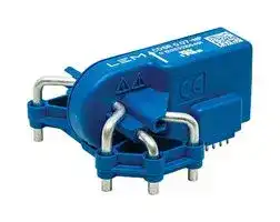
CDSR 0.07-NP
Current Transducer, Voltage, SPI Digital, 3.33V to 3.26V, −150mA to 150mA, 1ms, CDSR Series
⚠️ Reference pricing provided. In case of supply shortages, we will connect you with our trusted procurement partners to ensure your project's continuity.
- Manufacturer: LEM
- Product type: Current Sensors
- SVHC: No SVHC (25-Jun-2025)
- Accuracy: ± 8.3%
- Product Range: CDSR-NP Series
- Response Time: 1ms
- Primary Current: 70mA
- Sensor Mounting: Through Hole
- Measured Current: AC / DC / Pulsed
- Sensor Output Type: Voltage, SPI Digital
- Supply Voltage Range: 3.26V to 3.33V
- Secondary Signal Type: Voltage
- Supply Voltage DC Max: 3.33V
- Supply Voltage DC Min: 3.26V
- Current Sensor Technology: Open Loop, Flux Gate
- Operating Temperature Max: 85°C
- Operating Temperature Min: -40°C
- Current Measuring Range AC: -150mA to 150mA
- Current Measuring Range DC: -150mA to 150mA
| Delivery and price | |
|---|---|
| Units per pack | 50 |
| Price | 27.67 € |
| Current stock | 10+ |
| Lead time | 30 days |
Datasheet

## **Current Transducer CDSR 0.07-NP**

## _I_ **= 70 mA** P R N

For the electronic measurement of current: DC, AC, pulsed..., with galvanic separation between the primary and the secondary circuit.

## **Features**

- ●Open loop current transducer

- ●Voltage and SPI digital output

- ●Single supply voltage 3.3 V

- ●PCB mounting.

## **Special feature**

- ●Embedded primary jumpers.

## **Advantages**

- ●Very low error at small currents

- ●High overload capability

- ●High insulation capability

- ●Test winding.

## **Applications**

- ●Leakage current measurement in an IC-CPD in-cable (mode 2) and for wall boxes (mode 3) contact and protection device

- ●Single phase nominal current up to ±32 A RMS.

## **Complies with applications using these standards**

- ●IEC 61851-1: 2017

- ●IEC 62752: 2016

- ●IEC 62955: 2018

- ●UL 2231-1: 2012

- ●UL 2231-2: 2012

- ●UL 2594: 2016.

## **Application Domain**

- ●Residential.

N° 97.W7.Q5.000.0

Page 1/18 LEM International SA Route du Nant-d’Avril, 152 1217 Meyrin www.lem.com

LEM reserves the right to carry out modifications on its transducers, in order to improve them.

24November2022/Version 4

**CDSR 0.07-NP**

## **Safety**

## ⚠

## Caution

If the device is used in a way that is not specified by the manufacturer, the protection provided by the device may be compromised. Always inspect the electronics unit and connecting cable before using this product and do not use it if damaged. Mounting assembly shall guarantee the maximum primary busbar temperature, fulfill clearance and creepage distance, minimize electric and magnetic coupling, and unless otherwise specified can be mounted in any orientation

The plastic housing is conform to IK06 level (1 Joule). The device was certified for indoor use only and at an altitude below 2000 m.

## Caution, risk of electrical shock

This transducer must be used in limited-energy secondary circuits SELV according to IEC 61010-1, in electric/electronic equipment with respect to applicable standards and safety requirements in accordance with the manufacturer’s operating specifications. When operating the transducer, certain parts of the module can carry hazardous voltage (e.g. primary busbar, power supply). De-energize all circuits and hazardous live parts before installing the product.

All installations, maintenance, servicing operations and use must be carried out by trained and qualified personnel practicing applicable safety precautions.

If the transducer is used in a manner not specified by the manufacturer, the protection provided by the equipment may be impaired. Ignoring this warning can lead to injury and/or cause serious damage.

This transducer is a build-in device, whose hazardous live parts must be inaccessible after installation.

This transducer must be mounted in a suitable end-enclosure and its measuring jumpers must be at some point in the final installation protected behind a properly dimensioned circuit breaker that can be easily accessed by the end user of the application. Use caution during installation and use of this product; high voltages and currents may be present in circuit under test. Main supply must be able to be disconnected.

Never connect the output to any equipment with a common mode voltage to earth greater than 30 volts.

Always wear protective clothing and gloves if hazardous live parts are present in the installation where the measurement is carried out.

This transducer is a built-in device, not intended to be cleaned with any product. Nevertheless if the user must implement cleaning or washing process, validation of the cleaning program has to be done by himself.

## ESD susceptibility

The product is susceptible to be damaged from an ESD event and the personnel should be grounded when handling it. Do not dispose of this product as unsorted municipal waste. Contact a qualified recycler for disposal.

Although LEM applies utmost care to facilitate compliance of end products with applicable regulations during LEM product design, use of this part may need additional measures on the application side for compliance with regulations regarding EMC and protection against electric shock. Therefore LEM cannot be held liable for any potential hazards, damages, injuries or loss of life resulting from the use of this product.

Underwriters Laboratory Inc. recognized component

"This Arrow indicates the positive residual current measurement"

Page 2/18 LEM International SA Route du Nant-d’Avril, 152 1217 Meyrin www.lem.com

LEM reserves the right to carry out modifications on its transducers, in order to improve them.

24November2022/Version 4

**CDSR 0.07-NP**

## **Absolute maximum ratings**

**==> picture [511 x 23] intentionally omitted <==**

**----- Start of picture text -----**<br>
Parameter Symbol Unit Value<br>**----- End of picture text -----**<br>


|**Parameter**|**Symbol**|**Unit**|**Value**|
|---|---|---|---|
|||||
|Maximum supply voltage|±_U_C max|V|3.6|
|Maximum primary conductor temperature|_T_Bmax|°C|100|
|Maximum withstand primary peak current|_Î_P max|A|3300|
|Electrostatic discharge voltage (HBM - Human Body Model)|_U_ESD HBM|kV|6|


Absolute maximum ratings apply at 25 °C unless otherwise noted. Stresses above these ratings may cause permanent damage. Exposure to absolute maximum ratings for extended periods may degrade reliability.

## **UL 508: Ratings and assumptions of certification**

File # E189713 - Vol. 2.

## **Standards**

- ●CSA C22.2 NO. 14-10 INDUSTRIAL CONTROL EQUIPMENT - Date 2011/08/01

- ●UL 508 STANDARD FOR INDUSTRIAL CONTROL EQUIPMENT - Date 2013

- ●UL 61010

## **Ratings**

**==> picture [511 x 20] intentionally omitted <==**

**----- Start of picture text -----**<br>
Parameter Symbol Unit Value<br>**----- End of picture text -----**<br>


|**Parameter**|**Symbol**|**Unit**|**Value**|
|---|---|---|---|
|||||
|Primary involved potential||V RMS|300|
|Maximum surrounding air temperature|_T_A|°C|85|
|Primary current|_I_P|A|32|
|Secondary supply voltage|_U_C|V DC|3.3|
|Output voltage|_U_out|V|0 to 3.3|


## **Conditions of acceptability**

When installed in the end-use equipment, consideration shall be given to the following:

- _1 - These devices must be mounted in a suitable end-use enclosure._

- _2 -  The terminals have not been evaluated for field wiring._

- _3 - The CDSR xx-NP Series shall be used in a pollution degree 2 environment or better._

- _4 -  Low voltage circuits are intended to be powered by a circuit derived from an isolating source (such as a transformer, optical isolator, limiting impedance or electro-mechanical relay) and having no direct connection back to the primary circuit (other than through the grounding means).The maximum current supplied to the device must be protected/limited to a maximum of 5 Amperes._

- _5 -  These devices are intended to be mounted on the printed wiring board of the end-use equipment (with a minimum CTI of 100)._

- _6 -  CDSR xx-NP Series: based on results of temperature tests, in the end-use application, a maximum of 110°C cannot be exceeded on the primary jumper._

- _7 -  Primary feeder of the devices shall be connected after an overvoltage device or system which has been evaluated by the Standard for Transient Voltage Surge Suppressors, UL 1449 with a maximum clamping voltage of 6 kV._

## **Marking**

Only those products bearing the UL or UR Mark should be considered to be Listed or Recognized and covered under UL’s FollowUp Service. Always look for the Mark on the product.

## **Performances**

All described performances are valid for the whole temperature range at _U_ C = 3.3 V, unless otherwise noted.

Page 3/18 LEM International SA Route du Nant-d’Avril, 152 1217 Meyrin www.lem.com

LEM reserves the right to carry out modifications on its transducers, in order to improve them.

24November2022/Version 4

**CDSR 0.07-NP**

## **Insulation coordination**

**==> picture [512 x 24] intentionally omitted <==**

**----- Start of picture text -----**<br>
Parameter Symbol Unit ≤  Value Comment<br>**----- End of picture text -----**<br>


||**Symbol**|**Unit**|_≤_**Value**|_≤_**Value**|
|---|---|---|---|---|
||||||
|RMS voltage for AC insulation test, 50 Hz, 1 min|_U_d|kV|3.3|According to IEC 60664|
|Impulse withstand voltage 1.2/50 μs|_U_Ni|kV|6|According to IEC 60664|
|Partial discharge RMS test voltage (_q_m< 10 pC)|_U_t|V|825|According to IEC 60664|
|Clearance (pri. - sec.)|_d_CI|mm|10.15|Shortest distance through air|
|Creepage distance (pri. - sec.)|_d_Cp|mm|10.15|Shortest path along device body|
|Clearance (pri. - pri.)|_d_CI|mm|5.64|Shortest distance through air|
|Creepage distance (pri. - pri.)|_d_Cp|mm|5.64|Shortest path along device body|
|Case material|-|-|V0|According to UL 94|
|Comparative tracking index|_CTI_||600||
|Application example<br>RMS voltage line-to-neutral||V|300|Reinforced insulation according to<br>IEC 60664-1 or IEC 61010-1<br>CAT III, PD2|


## **Environmental and mechanical characteristics**

|**Parameter**|**Symbol**|**Unit**|**Min**|**Typ**|**Max**|**Comment**|
|---|---|---|---|---|---|---|
|Ambient operating temperature|_T_A|°C|−40||85||
|Ambient storage temperature|_T_A st|°C|−50||85||
|Relative humidity|_RH_|%||85|||
|Mass|_m_|g||32|||


Page 4/18 LEM International SA Route du Nant-d’Avril, 152 1217 Meyrin www.lem.com

LEM reserves the right to carry out modifications on its transducers, in order to improve them.

24November2022/Version 4

**CDSR 0.07-NP**

**General electrical data** (see Min, Max, typ, definition paragraph in page 6)

**==> picture [512 x 21] intentionally omitted <==**

**----- Start of picture text -----**<br>
Parameter Symbol Unit Min Typ Max Comment<br>**----- End of picture text -----**<br>


|**Parameter**|**Symbol**|**Unit**|**Min**|**Typ**|**Max**|**Comment**|
|---|---|---|---|---|---|---|
||||||||
|Primary nominal residual RMS current|_I_P R N|mA||70|||
|Primary residual current, measuring range|_I_P R M|mA|−150||150||
|Supply voltage⎓|_U_C|V|3.26|3.3|3.33|Note1)|
|Current consumption⎓|_I_C|mA|||50||
|Electrical ofset current referred to primary|_I_O E|mA||2|||
|Temperature coefcient of_I_O Ereferred to primary|_TCI_O E|µA/K|−5.5||5.5|For digital output|
||||−8||8|For analog output (taking into<br>account laboratory equipment<br>dispersion)|
|Magnetic ofset current (@_I_P R= 250 A)|_I_O M|mA||0.6|||
|Primary current common mode rejection ratio||dB|79|||Common mode current 32 A<br>RMS. Residual current 0 mA|


## **Analog output performances (common mode current = 0 A,** − **40 ... +85 °C,** _**U**_ **C = 3.3 V)**

|**Parameter**|**Symbol**|**Unit**|**Min**|**Typ**|**Max**|**Comment**|
|---|---|---|---|---|---|---|
|Nominal sensitivity|_S_N|V/A||8.79|||
|RMS noise current 1 Hz ... 2 kHz<br>referred to primary|_I_no|mA||0.11||@ 25 °C|
|Delay time to 90 % of the fnal output value for_I_P Nstep|_t_D 90|ms|||1||
|Frequency bandwidth (−3 dB)|_BW_|kHz||2|||
|Sum of sensitivity and linearity error 0 <_I_P< 6 mA|_ε_S L|mA|−0.5||0.5|Measurement integration time<br>10 NPLC (50 Hz)|
|Sum of sensitivity and linearity error 6_≤_ _I_P _≤_10 mA|_ε_S L|mA|−1||1||
|Sum of sensitivity and linearity error 10 mA <_I_P|_ε_S L|%_I_P|−10||10||


## **Digital high accuracy output performances (Common mode current = 0 A,** − **40 ... +85 °C,** _**U**_ **C = 3.3 V)**

**==> picture [512 x 22] intentionally omitted <==**

**----- Start of picture text -----**<br>
Parameter Symbol Unit Min Typ Max Comment<br>**----- End of picture text -----**<br>


|**Parameter**|**Symbol**|**Unit**|**Min**|**Typ**|**Max**|**Comment**|
|---|---|---|---|---|---|---|
||||||||
|Nominal sensitivity|_S_N|LSB/mA||87.99|||
|Sum of sensitivity and linearity error 0 <_I_P< 6 mA|_ε_S L|mA|−0.5||0.5|Measurement integration time<br>10 NPLC (50 Hz)|
|Sum of sensitivity and linearity error 6_≤_ _I_P _≤_10 mA|_ε_S L|mA|−1||1||
|Sum of sensitivity and linearity error 10 mA <_I_P|_ε_S L|%_I_P|−10||10||
|Delay time to 90 % of the fnal output value for_I_P Nstep|_t_D 90|ms|||40|Not including SPI time frame|
|Frequency bandwidth (−3 dB)|_BW_|Hz||10|||


## − **Digital high bandwidth output performances (Common mode current = 0 A, 40 ... +85 °C,** _**U**_ **C = 3.3 V)**

**==> picture [512 x 22] intentionally omitted <==**

**----- Start of picture text -----**<br>
Parameter Symbol Unit Min Typ Max Comment<br>**----- End of picture text -----**<br>


|**Parameter**|**Symbol**|**Unit**|**Min**|**Typ**|**Max**|**Comment**|
|---|---|---|---|---|---|---|
||||||||
|Nominal sensitivity|_S_N|LSB/mA||87.99|||
|Sum of sensitivity and linearity error 0 <_I_P< 6 mA|_ε_S L|mA|−1||1|Measurement integration time<br>2 NPLC (50 Hz)|
|Sum of sensitivity and linearity error 6_≤_ _I_P _≤_10 mA|_ε_S L|mA|−1||1||
|Sum of sensitivity and linearity error 10 mA <_I_P|_ε_S L|%_I_P|−10||10||
|Delay time to 90 % of the fnal output value for_I_P Nstep|_t_D 90|ms|||1|Not including SPI time frame|
|Frequency bandwidth (−3 dB)|_BW_|kHz||2|||


Note:[1) ] The sensitivity of the transducer depends on the power supply ( _U_ C) accuracy. A variation of 1 % of _U_ C may lead to a sensitivity drift of 1 %.

Page 5/18 LEM International SA Route du Nant-d’Avril, 152 1217 Meyrin www.lem.com

LEM reserves the right to carry out modifications on its transducers, in order to improve them.

24November2022/Version 4

**CDSR 0.07-NP**

## **Definition of typical, minimum and maximum values**

Minimum and maximum values for specified limiting and safety conditions have to be understood as such as well as values shown in “typical” graphs.

On the other hand, measured values are part of a statistical distribution that can be specified by an interval with upper and lower limits and a probability for measured values to lie within this interval.

Unless otherwise stated (e.g. “100 % tested”), the LEM definition for such intervals designated with “min” and “max” is that the probability for values of samples to lie in this interval is 99.73 %.

For a normal (Gaussian) distribution, this corresponds to an interval between −3 sigma and +3 sigma. If “typical” values are not obviously mean or average values, those values are defined to delimit intervals with a probability of 68.27 %, corresponding to an interval between −sigma and +sigma for a normal distribution.

Typical, maximal and minimal values are determined during the initial characterization of the product.

Page 6/18 LEM International SA Route du Nant-d’Avril, 152 1217 Meyrin www.lem.com

LEM reserves the right to carry out modifications on its transducers, in order to improve them.

24November2022/Version 4

**CDSR 0.07-NP**

## **Digital signals electrical parameters**

**==> picture [511 x 22] intentionally omitted <==**

**----- Start of picture text -----**<br>
Parameter Symbol Unit Min Typ Max Comment<br>**----- End of picture text -----**<br>


|**Parameter**|**Symbol**|**Unit**|**Min**|**Typ**|**Max**|**Comment**|
|---|---|---|---|---|---|---|
||||||||
|Input logic low|_U_in L|V|−0.3||0.8||
|Input logic high|_U_in H|V|2||_U_C+<br>0.2||
|Output logic low|_U_out L|V|||0.4||
|Output logic high|_U_out H|V|_U_C− 0.4||||
|Sink / drive output maximum current|_I_out max|mA|−4||4||


## **General switching parameters**

**==> picture [511 x 22] intentionally omitted <==**

**----- Start of picture text -----**<br>
Parameter Symbol Unit Min Typ Max Comment<br>**----- End of picture text -----**<br>


|**Parameter**|**Symbol**|**Unit**|**Min**|**Typ**|**Max**|**Comment**|
|---|---|---|---|---|---|---|
||||||||
|Start-up time|_t_start|ms|||100|Also valid after a reset pulse|
|Minimum reset time|_t_res min|µs|5||||
|Frequency of fault output|_f_out fault|kHz|11||21||
|Fault signal threshold|_I_Th|mA|152||175||
|Fault signal reaction time|_t_fault|µs|||200||


## **Serial interface switching parameters and format**

|**Parameter**|**Parameter**|**Parameter**|**Parameter**|**Parameter**|**Parameter**|**Symbol**|**Symbol**|**Symbol**|**Symbol**|**Symbol**|**Symbol**|**Unit**|**Min**|**Min**|**Min**|**Typ**|**Typ**|**Typ**|**Max**|**Max**|**Max**|**Max**|**Comment**|**Comment**|**Comment**|
|---|---|---|---|---|---|---|---|---|---|---|---|---|---|---|---|---|---|---|---|---|---|---|---|---|---|
|Delay to valid SCLK||||||_t_SS SCL||||K||ns|100|||||||||||||
|Delay time, fnal SCLK falling edge to<br>SS rising edge||||||_t_SCLK S||||S||ns|100|||||||||||||
|Pulse duration, SS high||||||_t_SS H||||||ns|200|||||||||||||
|SCLK period||||||_t_per SCL||||K||ns|250|||||||||||||
|Pulse duration, SCLK high||||||_t_PW SCLK||||H||ns|100|||||||||||||
|Pulse duration, SCLK low||||||_t_PW SCL||||K L||ns|100|||||||||||||
|Hold time, SCLK rising edge to<br>MISO invalid||||||_t_hold MIS||||O||ns|0|||||||||||||
|SS<br>SCLK<br>MISO||||||||||||||||||||||||||
|||||||||||||||||||||||||||
||_t_|_t_||||||||||||||||||||||||
||S|S SCLK<br>per SCLK||||||||||||_t_PW SCLK H||||||||||_t_SCLK SS||
|||||||||||||||||||||||||||
||Hi-Z<br>|_t_SS MISO D||||||||||||||||||||||||
|||||||||||||||||||||||||||


Figure 1

Page 7/18 LEM International SA Route du Nant-d’Avril, 152 1217 Meyrin www.lem.com

LEM reserves the right to carry out modifications on its transducers, in order to improve them.

24November2022/Version 4

**CDSR 0.07-NP**

## **SPI Communication**

## **Normal operation**

**==> picture [512 x 224] intentionally omitted <==**

**----- Start of picture text -----**<br>
SPI word N°1 SPI CRC BYTE<br>16 bits word N°2<br>16 bits word N°1 high bandwidth Error control<br>high accuracy<br>Overcurrent situation/HW fault situation<br>SPI word N°1 SPI CRC BYTE<br>All '1' Don't care Error control<br>Bit Nb 15                       6       5        4          3         2         1         0<br>All '1'  = '0'   = '0'   = '1'   = '0'  = '1'  = '1'<br>alert for current  RFU1* RFU0* HW  out of  critical<br>measure error Fault range  overload<br>residual  residual<br>current** current<br>SPI word N°2<br>SPI word N°2<br>**----- End of picture text -----**<br>


- RFU = Reserved for Future Use

- ** see "Fault signal threshold" min/max values.

## **SPI management**

The transducer's SPI is defined as mode 1 (CPOL = 0 , CPHA = 1, CKE/NCPHA = 0). The transducer will be always in slave configuration and half-duplex communication.

The Chip Select and Serial Clock must be generated by the master (User).

The dynamic time parameter for the SPI communication are indicated in a parameter table (see above page for more details). The transducer complete SPI command is composed of 5 bytes, defined as follows:

- -2 bytes Word No1: digital high-Bandwidth output.

- -2 bytes Word No2: digital high-Accuracy output.

-1-byte Checksum CRC error detection:

The 1-byte CRC-8 Error detection is computed using the CRC-8-CCITT polynomial :

_x_ 8 + _x_ 2 + _x_ + 1

Each of the 5 bytes from the SPI data frame will have to be fed (Most Significant Byte first) to a “crc8” function as in the hereunder pseudo-code. Note that the initial CHECKSUM value is set to 0xFF:

CHECKSUM = 0xFF;

CHECKSUM = crc8(CHECKSUM, SPI_BYTE_1); CHECKSUM = crc8(CHECKSUM, SPI_BYTE_2); CHECKSUM = crc8(CHECKSUM, SPI_BYTE_3); CHECKSUM = crc8(CHECKSUM, SPI_BYTE_4); CHECKSUM = crc8(CHECKSUM, SPI_BYTE_5);

The expected CHECKSUM value at the end shall be 0x00 if no transmission error occurred. The crc8 function must be coded in the following way (example given C language): unsigned char crc8( unsigned char crc_in, unsigned char data_in) { unsigned char i; unsigned char data; data = crc_in ^ data_in; for ( i = 0; i < 8; i++ ) { if (( data & 0x80 ) != 0 ) { data <<= 1; data ^= 0x07; } else { data <<= 1; } } return data; }

24November2022/Version 4

Page 8/18 LEM International SA Route du Nant-d’Avril, 152 1217 Meyrin www.lem.com

LEM reserves the right to carry out modifications on its transducers, in order to improve them.

**CDSR 0.07-NP**

For reference, here is the CRC-8 calculation results for an example SPI data frame:

-- SPI data frame content: SPI_BYTE_1 = 0x83 SPI_BYTE_2 = 0x20 SPI_BYTE_3 = 0xE3 SPI_BYTE_4 = 0x96 SPI_BYTE_5 = 0x0E

-- checksum calculation: CHECKSUM = 0xFF; crc8(0xFF, 0x83) => CHECKSUM = 0x73 crc8(0x73, 0x20) => CHECKSUM = 0xBE crc8(0xBE, 0xE3) => CHECKSUM = 0x94 crc8(0x94, 0x96) => CHECKSUM = 0x0E crc8(0x0E, 0x0E) => CHECKSUM = 0x00

The final CHECKSUM value = 0x00: There were no communication error.

## **Error definition**

## **Digital output**

The Transducer detects 3 potential hazardous situations:

- 1)  “out-of-range residual current” (measured residual current higher than specified Fault Signal threshold. Internally the transducer is still capable of calculating residual current as in normal operation, but without guaranteeing error min/max tolerance)

- 2)  “critical residual current overload” (in this case, the residual current is high enough for preventing the transducer to function correctly and calculate any residual current).

- 3)  “HW fault” (when the internal HW self check has raised an error flag). This flag will be kept raised until the next device power cycle.

When any of above error are detected, the SPI command changes based on following definition:

*16-bits word N°1:

- -vector slice bit 15 -MSB- down to bit 6: are set to logic '1' value.

- -bit 5: don’t care, reserved for future use.

- -bit 4: don’t care, reserved for future use.

- -bit 3: set to logic ‘1’ when “HW fault” is detected.

- -bit 2: set to logic ‘0’ value.

- -bit 1 : set to logic ‘1’ value when “out-of-range residual current” is measured.

- -bit 0: set to logic ‘1’ value when “critical residual current overload” is detected.

- 16-bits word N°2: High accuracy stream. This data should not be considered in the event of an error detection.

- 8-bits CRC byte: Error control byte.

Here below an example of error communication where only the first 16 bits have been represented (in this example, a residual current out of range has been detected):

|**BIT NUMBER**|**15**|**14**|**13**|**12**|**11**|**10**|**9**|**8**|**7**|**6**|**5**|**4**|**3**|**2**|**1**|**0**|
|---|---|---|---|---|---|---|---|---|---|---|---|---|---|---|---|---|
|**BIT VALUE**|**1**|**1**|**1**|**1**|**1**|**1**|**1**|**1**|**1**|**1**|**0**|**0**|**0**|**0**|**1**|**0**|


## **Analog output**

The same 16-bit word N°1 is the input value of the First-Order Sigma-Delta modulator used for the analog output (see pin 3 and 6 definition).

Therefore, error can also be detected by the analog output.

Page 9/18 LEM International SA Route du Nant-d’Avril, 152 1217 Meyrin www.lem.com

LEM reserves the right to carry out modifications on its transducers, in order to improve them.

24November2022/Version 4

**CDSR 0.07-NP**

## **Performance parameters definition**

## **Magnetic offset referred to primary**

The magnetic offset current on the primary side (“memory effect” of the transducer’s ferro- _I_ O M is the consequence of a current magnetic parts). It is measured using the following primary current cycle. _I_ O M depends on the current value _I_ P R _≥ I_ P R N.

## _K_ OL: Overload factor

**==> picture [224 x 133] intentionally omitted <==**

**----- Start of picture text -----**<br>
Primary current cycle<br>1<br>0<br>-1<br>1 2 3 4 5<br>Step<br>)N<br>P<br>I ·<br>OL  = 1 .. 10<br>K OL<br> ( / K<br>P R<br>I with<br>**----- End of picture text -----**<br>


## **Delay times**

respect to the primary are shown in the next figure.The delay time _t_ D 10 to 10 % and the delay time _t_ D 90 @ 90 % with Both slightly depend on the primary current d _i_ /d _t_ . They are measured at nominal current.

**==> picture [169 x 115] intentionally omitted <==**

**----- Start of picture text -----**<br>
I<br>100 %<br>90 %<br>I P U out<br>t D 90<br>10 %<br>t D 10 t<br>**----- End of picture text -----**<br>


Figure 3: _t_ D 10 (delay time to 10 %) and _t_ D 90 (delay time @ 90 %).

Figure 2:  Current cycle used to measure magnetic and electrical offset (transducer supplied)

**==> picture [96 x 25] intentionally omitted <==**

## **Electrical offset referred to primary**

Using the current cycle shown in figure 2, the electrical offset current _I_ O E is the residual output referred to primary when the input current is zero.

**==> picture [92 x 26] intentionally omitted <==**

The temperature variation _I_ O _T_ of the electrical offset current _I_ O E is the variation of the electrical offset from 25 °C to the considered temperature.

_U_ O _T_ ( _T_ ) = _U_ O E ( _T_ ) − _U_ O E (25 °C)

Page 10/18 LEM International SA Route du Nant-d’Avril, 152 1217 Meyrin www.lem.com

LEM reserves the right to carry out modifications on its transducers, in order to improve them.

24November2022/Version 4

**CDSR 0.07-NP**

## **CDSR typical mounting and interfacing**

**==> picture [461 x 202] intentionally omitted <==**

**----- Start of picture text -----**<br>
primary jumpers<br>16 P1_In P1_Out 12<br>Test voltage source 470R 1718 P2_InP3_In P2_OutP3_Out 1314<br>PTVS4V5D1BL 15 N_In N-Out 11<br>or equivalent ** Positive Residual Current<br>GND 21 Test_inGND<br>Analog measurements Analog_pos 4k7* 4k7* 33R 345 Analog_posUcRESET<br>Analog_neg 1nF*4k7* 1nF*4k7* 1nF* 1nF* 33R33R33R33R 106789 Analog_negFaultSSSCLKMISO CDSR-NP<br>Digital measurements Uc<br>GND<br>* To be placed as close as possible to the transducer 47uF* 100nF* 10nF*<br>** Equivalence with PTVS4V5D1BL must respect following criteria:<br>-Robustness against IEC 61000-4-5 8/20 µs current waveform.<br>-Maximum clamping voltage < 20V under 8/20us waveform test. GND<br>-Breakdown voltage / Reverse standoff voltage > 4V.<br>-Bidirectionnal protection.<br>1<br>2<br>**----- End of picture text -----**<br>


**==> picture [134 x 18] intentionally omitted <==**

**----- Start of picture text -----**<br>
Pin N° Function<br>**----- End of picture text -----**<br>


|1|Test_in|
|---|---|
|2|GND|
|~~3~~|Analog_pos|
|4|_U_C|
|||
|~~5~~|~~Reset~~|
|6|Analog_neg|
|7|Fault|
|8|SS|
|9|SCLK|
|10|MISO|


## *** Pin de** ~~**scrip**~~ **ti** ~~**on:**~~

~~Pin No 1 'Test~~ _ ~~in':~~ Th ~~i~~ s ~~p~~ in i ~~s conn~~ ected t ~~o~~ a 10-turns coil ~~.~~ It pe ~~r~~ mits the use ~~r~~ to ~~c~~ heck periodically the transducer

~~perform~~ ance ~~b~~ y inj ~~e~~ cting a precise curr ~~en~~ t thr ~~o~~ ug ~~h~~ the pin.The other coil end terminal is connected to the transducer ground.

Pin No 2 'GND': Ground. Pin No 3 'Analog_pos': 48 MHz Sigma-Delta bitstream to be filter ~~ed~~ . ~~P~~ in No 4 ' ~~_U_ C~~ ': Power supply.

~~Pin No 5 'Reset~~ ' ~~: Active low-level reset signal. Plea~~ se refer to Start-up time ( _t_ start) for ~~n~~ ominal ~~operation.~~ Pin No 6 'Analog_neg': Inver ~~te~~ d signal of pin No 3 ' ~~A~~ nalo ~~g~~ _pos'. Pin ~~No~~ 7 'Fault': See "Fault p ~~in~~ Signal" parag ~~r~~ aph page 14. Pin No 8 'SS': SPI active low-level Chip Select sign ~~al.~~ Pin No 9 'SCLK': SPI Serial Clock signal. Pin No 10 'MISO': SPI MISO signal.

Page 11/18 LEM International SA Route du Nant-d’Avril, 152 1217 Meyrin www.lem.com

LEM reserves the right to carry out modifications on its transducers, in order to improve them.

24November2022/Version 4

**CDSR 0.07-NP**

## **Example of CDSR output readings**

## **Analog output**

The analog current measurement is provided on pin 3 and 6 by a differential 48 Mhz Sigma-Delta bitstream to be filtered. User must apply identical low-pass filtering to both outputs. The first stage (R = 4.7k/C = 1 nF) of a 3rd order hardware low pass filter is already embedded into the transducer. 2 last stages are added for analog output measurements. Refer to “CDSR typical mounting and interfacing” for typical HW design.

The cutoff frequency of the described filter is 6.4 kHz, compatible with a 2 kHz output bandwidth.

Primary residual current conversion from analog samples is described in below equation:

> (analog positive [ _mV_ ] − analog negative [ _mV_ ] − initial offset compensation [ _mV_ ]

> Primary residual current mA [ ] =

> Nominal sensitivity [ _mV_ / _mA_ ]

## **Initial analog offset compensation:**

The first current measurement done after the transducer start-up should be used for an initial offset compensation. Consecutive transducer residual current reading must be compensated by the initial offset.

## Here below an example of reading operation:

After start-up, residual current _I_ primary = 0 mA (user must be certain there is no residual current when initial offset compensation is applied).

Analog voltage reading (measurement should ideally be integrated over 10 NPLC): _U_ (analog_pos) − _U_ (analog_neg) = _U_ 0 = 2.2 mV.

Injected residual current I primary = 10 mA.

New analog voltage reading: _U_ (analog_pos) − _U_ (analog_neg) = _U_ 1 = 90 mV.

After applying initial offset compensation _U_ compensated = _U_ 1 − _U_ 0 = 87.8 mV.

Conversion to primary current:

_I_ = _U_ compensated / 8.79 [mV/mA] = 9.984 mA.

## **Digital output**

The SPI’s digital data-frame provides the user with 2 measurements 16 bits words: “High bandwidth” and “High accuracy”. The high accuracy word (limited to 10 Hz bandwidth) can be used for DC measurement. The high bandwidth can be used for AC measurement.

While both words have the exact same source of data, the fundamental difference between the 2 words is their respective bandwidth. The "high accuracy" word, with a 10 Hz bandwidth is the digitally filtered image of the "high bandwidth" word of 2 kHz bandwidth. The "High accuracy" word can be used to subtract the DC component from the residual current measurement of the "high bandwidth" word. Therefore, the "high accuracy" word should be used to detect smooth DC residual currents while the "high bandwidth" should rather be used to measure and compute AC RMS residual currents.

The SPI’s digital samples are coded on a 16 bits full-scale (i.e from 0LSB to 65535LSB). Because both positive and negative residual currents can be measured by the transducer, the 0 mA residual current value is centered @ 50 % of the full scale

216 ( = 32768). 2

Therefore the SPI’s digital samples must always be subtracted with 32768LSB before converting the value into primary residual current as described in below equation:

Here below an example of reading operation for the digital high-bandwidth value:

> (Digital sample [ _LSB_ ] − 32768) − initial offset compensation [ _LSB_ ]

> Primary residual current mA [ ] =

> Nominal sensitivity [ _LSB_ / _mA_ ]

## After start-up,

_I_ primary = 0 mA

‘Digital sample’ _D_ 0 = 32814 LSB (the 16-bits word converted to decimal)

216 = 32768) 2

Subtracting center value 50 % of 16 bits full-scale ( = 32768) 2 Conversion to primary current (ignoring initial offset compensation value for the sake of this example): _D_ 1 = _D_ 0 − 32768 = 46 LSB. _I_ = 46 LSB / 87.99 LSB/mA = 0.522 mA

Page 12/18 LEM International SA Route du Nant-d’Avril, 152 1217 Meyrin www.lem.com

24November2022/Version 4 LEM reserves the right to carry out modifications on its transducers, in order to improve them.

**CDSR 0.07-NP**

## **Initial digital offset compensation:**

Likewise the analog output reading, an initial offset compensation must be applied onto the digital stream after each transducer start-up. It is strongly recommended to perform initial offset compensation based on the “high accuracy” stream.

Here below an example of reading operation:

After start-up, residual current _I_ primary = 0 mA (user must be certain there is no residual current when initial offset compensation is applied).

Digital "High accuracy" stream sampling(sampling should ideally be performed over 10 NPLC and then averaged): Digital sample −32768 = _D_ 0 = 45 LSB = initial offset compensation value.

Injected residual current _I_ primary = 10 mA.

New digital “High bandwidth” and “High accuracy” readings:

High bandwidth sample −32768 = _D_ 1 −32768 = 920 LSB High accuracy sample −32768 = _D_ 2 −32768 = 923 LSB.

After applying initial offset compensation : High bandwidth sample offset compensated = 920 − 45 = 875 LSB High accuracy sample offset compensated = 923 − 45 = 878 LSB.

Conversion to primary current:

875 _LSB_ High bandwidth primary current sample = = 9.94 mA 87.99 _LSB_ / mA 878 _LSB_ High accuracy primary current sample = = 9.98 mA 87.99 _LSB_ / mA

## **General recommendations for analog and digital sampling rates:**

Both analog stream and “High bandwidth” digital stream have a 2 kHz bandwidth.

It is recommended to acquire samples at a minimum rate of 8 kSa/s or even further for proper RMS calculations.

This can be achieved using DMA-driven SPI/analog acquisition HW so such feature should be strongly considered on a system level.

Page 13/18 LEM International SA Route du Nant-d’Avril, 152 1217 Meyrin www.lem.com

LEM reserves the right to carry out modifications on its transducers, in order to improve them.

24November2022/Version 4

**CDSR 0.07-NP**

## **Fault-pin Signal**

Dynamic diagnostic signal: when a fault is detected the signal remains in any steady state (can be a logic low (0) or high (1)).

Detected faults:

- ●Over-current

- ●Critical over-current

- ●Internal hardware self-test

Figure 4: Fault-pin signal illustration

## **“Test-in” pin**

The “Test in” pin is connected to a 10 turns coil inside the transducer: 1 mA injected to this pin will result in 10 mA measurement. This enables users to test the transducer.

Due to transformer effect a high impedance source is required to generate the test current. Below an example of a 3.3 mA current generation in the test coil.

Figure 5: "Test-in" pin illustration

It is also required to connect a bidirectional protection device in order to protect the user PCBA against hazardous transient high pulse current through the primary jumper.

Standard Transient Voltage suppressor could accomplish this function (voltage rating to be defined based on specific user application but has to be > 4 V not to perturbate the transducer proper functioning). See CDSR typical mounting and interfacing on page 11.

Page 14/18 LEM International SA Route du Nant-d’Avril, 152 1217 Meyrin www.lem.com

LEM reserves the right to carry out modifications on its transducers, in order to improve them.

24November2022/Version 4

**CDSR 0.07-NP**

## **PCB footprint**

**==> picture [239 x 232] intentionally omitted <==**

Note: The dimension of customer PCB tracks (width & thickness) and the LEM transducer’s primary jumpers are linked and can influence on each other regarding thermal exchanges and self heating.

## **Assembly on PCB**

- ●Recommended PCB hole diameter

- ●Recommended primary via ring diameter:

- ●Wave soldering profile No clean process only

⌀ 3.3 mm +0.15 mm/−0 mm for primary pin

⌀ 1.4 mm +0.15 mm/−0 mm for secondary pin min 3.9 mm maximum 260 °C, 10 s

Page 15/18 LEM International SA Route du Nant-d’Avril, 152 1217 Meyrin www.lem.com

LEM reserves the right to carry out modifications on its transducers, in order to improve them.

24November2022/Version 4

**CDSR 0.07-NP**

**Dimensions** (in mm, general tolerance ±0.6 mm)

**==> picture [512 x 565] intentionally omitted <==**

**----- Start of picture text -----**<br>
d Cl d Cp Connectio n<br>10.15 10.15<br>**----- End of picture text -----**<br>


Page 16/18 LEM International SA Route du Nant-d’Avril, 152 1217 Meyrin www.lem.com

LEM reserves the right to carry out modifications on its transducers, in order to improve them.

24November2022/Version 4

**CDSR 0.07-NP**

## **Creepage and Clearance**

**==> picture [512 x 365] intentionally omitted <==**

Page 17/18 LEM International SA Route du Nant-d’Avril, 152 1217 Meyrin www.lem.com

LEM reserves the right to carry out modifications on its transducers, in order to improve them.

24November2022/Version 4

**CDSR 0.07-NP**

## **Packaging information**

Standard delivery in cardboard:  L × W × H: 300 × 200 × 200 mm

Each cardboard contains 60 parts, placed into 5 Polystyrene-made trays of 12 parts each one. Both trays and cardboard are ESD-compliant. The typical weight of the cardboard is 3.3 Kg.

Page 18/18 LEM International SA Route du Nant-d’Avril, 152 1217 Meyrin www.lem.com

LEM reserves the right to carry out modifications on its transducers, in order to improve them.

24November2022/Version 4
Updated at June 10, 2026
About Novapart
Novapart is a B2B electronic component broker specialising in stock shortages and cost reduction. We source hard-to-find parts and identify compliant alternatives across a catalogue of 410,000+ components from 500+ manufacturers.
Learn more →Stock Shortage Specialist
When a component is unavailable, discontinued or has an unacceptable lead time, we tap into our network of vetted European and Asian distributors to source what you need — without compromising on quality or traceability.
Request a quote →Compliant Alternatives
We identify pin-to-pin, electrically equivalent substitutes that meet the same certifications (RoHS, AEC-Q100, REACH) as your original specification — validated against datasheets, not just part numbers. Often at a lower cost.
BOM Analysis service →