


CD214A-B340R
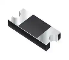
Schottky Rectifier, 40 V, 3 A, Single, DO-214AC (SMA), 2 Pins, 500 mV
- Manufacturer: BOURNS
- Product type: Schottky Rectifier Diodes
- Repetitive Reverse Voltage Vrrm Max:40V; Forward Current If(AV):3A; Diode Configuration:Single; Diode Case Style:DO-214AC; No. of Pins:2Pins; Forward Voltage VF Max:500mV; Forward Su
- SVHC: Lead (04-Feb-2026)
- No. of Pins: 2Pins
- Product Range: CD214A-B3xR
- Qualification: -
- Diode Mounting: Surface Mount
- Diode Case Style: DO-214AC (SMA)
- Diode Configuration: Single
- Forward Voltage Max: 500mV
- Forward Surge Current: 80A
- Average Forward Current: 3A
- Operating Temperature Max: 125°C
- Repetitive Peak Reverse Voltage: 40V
| Delivery and price | |
|---|---|
| Units per pack | 5000 |
| Price | 0.151 € |
| Current stock | 1000+ |
| Lead time | 30 days |
**==> picture [44 x 43] intentionally omitted <==**

**----- Start of picture text -----**<br>
*RoHS COMPLIANT<br>**----- End of picture text -----**<br>


## **Features**

n RoHS compliant* n Low profile n Low power loss, high efficiency n UL 94V-0 classification

## **Applications**

n Switch Mode Power Supplies n Portable equipment batteries n High frequency rectification n DC/DC Converters n Telecommunications

## BOURNS ~~IA~~ **CD214A-B3xR Series Schottky Barrier Rectifier Chip Diode**

## ~~**General Information**~~

Portable communications, computing and video equipment manufacturers are challenging the semiconductor industry to develop increasingly smaller electronic components.

Bourns offers Schottky Rectifier Diodes for rectification applications, in a compact chip package compatible with DO-214AC (SMA) size format. The Schottky Rectifier Diodes offer a forward current of 3 A with a choice of repetitive peak reverse voltage of 20 V up to 60 V.

## ~~**Absolute Maximum Ratings (@ TA = 25 °C Unless Otherwise Noted)**~~

|**Parameter**|**Symbol**|**CD214A-**|**CD214A-**|**CD214A-**|**CD214A-**|**CD214A-**|**Unit**|
|---|---|---|---|---|---|---|---|
|||**B320R**|**B320LR**|**B340R**|**B340LR**|**B360R**||
|Maximum Repetitive Peak Reverse Voltage|VRRM|20|20|40|40|60|V|
|Maximum Average Forward Current|IF(AV)|3|||||A|
|Maximum Peak Forward Surge Current<br>(8.3 ms Single Half Sine-Wave)|IFSM|80|||||A|
|Operating Junction Temperature Range|TOPR|-55 to +125|||||°C|
|Storage Temperature Range|TSTG|-55 to +150|||||°C|


## ~~**Electrical Characteristics (@ TA = 25 °C Unless Otherwise Noted)**~~

|**Parameter**<br>~~a~~|**Symbol**|**Condition or Model**|**Condition or Model**|**Min.**|**Typ.**|**Max.**|**Unit**|
|---|---|---|---|---|---|---|---|
|Maximum Instantaneous Forward Voltage<br> (NOTE 1)|VF|IF = 1 A<br>~~—~~|CD214A-B320R<br>CD214A-B340R<br>~~—~~||0.37||V<br>~~a~~<br>~~a~~<br>~~a~~|
||||CD214A-B360R<br>~~—~~<br>~~a~~|~~a~~|0.42<br>~~a~~|~~a~~||
||||CD214A-B320LR<br>CD214A-B340LR<br>~~—~~<br>~~a~~<br>~~a~~|~~a~~<br>~~a~~|0.3<br>~~a~~<br>~~a~~|~~a~~<br>~~a~~||
|||IF = 3 A<br>~~—~~|CD214A-B320R<br>CD214A-B340R<br>~~—~~|~~—~~|0.46<br>~~—~~|0.5<br>~~—~~||
||||CD214A-B360R<br>~~—~~<br>~~a~~|~~—~~<br>~~a~~|0.58<br>~~—~~<br>~~a~~|0.7<br>~~—~~<br>~~a~~||
||||CD214A-B320LR<br>CD214A-B340LR<br>~~—~~|~~—~~|0.39<br>~~—~~|0.42<br>~~—~~||
|DC Reverse Current<br>~~PR~~|IR<br>~~PR~~|VR =<br>VRRM<br>~~—~~<br>~~PR~~|CD214A-B320R<br>CD214A-B340R<br>CD214A-B360R<br>~~—~~<br>~~Sf~~<br>~~PR~~|~~—~~<br>~~Sf~~<br>~~PR~~|0.02<br>~~—~~<br>~~Sf~~<br>~~PR~~|0.2<br>~~—~~<br>~~Sf~~<br>~~PR~~|mA<br>~~PR~~|
||||CD214A-B320LR<br>CD214A-B340LR<br>~~PR~~|~~PR~~|0.55<br>~~PR~~|1<br>~~PR~~||
|Typical Junction Capacitance<br>~~PR~~|CJ<br>~~PR~~|VR =<br>4 V,<br>f = 1.0<br>MHz<br>~~PR~~|CD214A-B320R<br>CD214A-B340R<br>~~PR~~|~~PR~~|160<br>~~PR~~|~~PR~~|pF<br>~~PR~~<br>~~a~~<br>~~i~~|
||||CD214A-B360R<br>~~a~~|~~a~~|135<br>~~a~~|~~a~~||
||||CD214A-B320LR<br>CD214A-B340LR<br>~~i~~|~~i~~|120<br>~~i~~|~~i~~||


NOTE: (1) Pulse width 300 microsecond, 1 % duty cycle.

*RoHS Directive 2015/863, Mar 31, 2015 and Annex. Specifications are subject to change without notice.

The device characteristics and parameters in this data sheet can and do vary in different applications and actual device performance may vary over time. Users should verify actual device performance in their specific applications.

## **CD214A-B3xR Series Schottky Barrier Rec ifier Chip Diode3312 - 2 mm SMD Trimming Potentiometer**

||**3312 - 2 mm SMD Trimming Potentiometer**<br>**CD214A-B3xR Series Schottky Barrier Rec ifer Chip Diode**|**3312 - 2 mm SMD Trimming Potentiometer**<br>**CD214A-B3xR Series Schottky Barrier Rec ifer Chip Diode**|**3312 - 2 mm SMD Trimming Potentiometer**<br>**CD214A-B3xR Series Schottky Barrier Rec ifer Chip Diode**|**3312 - 2 mm SMD Trimming Potentiometer**<br>**CD214A-B3xR Series Schottky Barrier Rec ifer Chip Diode**|**3312 - 2 mm SMD Trimming Potentiometer**<br>**CD214A-B3xR Series Schottky Barrier Rec ifer Chip Diode**|**3312 - 2 mm SMD Trimming Potentiometer**<br>**CD214A-B3xR Series Schottky Barrier Rec ifer Chip Diode**|**3312 - 2 mm SMD Trimming Potentiometer**<br>**CD214A-B3xR Series Schottky Barrier Rec ifer Chip Diode**|**3312 - 2 mm SMD Trimming Potentiometer**<br>**CD214A-B3xR Series Schottky Barrier Rec ifer Chip Diode**|
|---|---|---|---|---|---|---|---|---|
||~~**Electrical Characteristics (@ TA = 25 °C Unless Otherwise Noted)**~~<br>**Parameter**<br>**Symbol**<br>**Condition or Model**<br>**Min.**<br>**Typ.**<br>**Max.**<br>**Unit**<br>Typical Thermal Resistance<br>(NOTE 2)<br>Junction to<br>Ambient<br>RθJA<br>CD214A-B320R<br>CD214A-B340R<br>CD214A-B360R<br>86<br>°C/W<br>CD214A-B320LR<br>CD214A-B340LR<br>55<br>Junction to<br>Lead<br>RθJL<br>CD214A-B320R<br>CD214A-B340R<br>CD214A-B360R<br>24<br>CD214A-B320LR<br>CD214A-B340LR<br>17||||||||
||**Parameter**||**Symbol**|**Condition or Model**|**Min.**|**Typ.**|**Max.**|**Unit**|
||Typical Thermal Resistance<br>(NOTE 2)|Junction to<br>Ambient|RθJA|CD214A-B320R<br>CD214A-B340R<br>CD214A-B360R||86||°C/W|
|||||CD214A-B320LR<br>CD214A-B340LR||55|||
|||Junction to<br>Lead|RθJL|CD214A-B320R<br>CD214A-B340R<br>CD214A-B360R||24|||
|||||CD214A-B320LR<br>CD214A-B340LR||17|||


NOTE: (2) Mounted on PCB with 5.0 x 5.0 mm (0.2 x 0.2 inch) copper pad areas.

Specifications are subject to change without notice. The device characteristics and parameters in this data sheet can and do vary in different applications and actual device performance may vary over time. Users should verify actual device performance in their specific applications.

## **CD214A-B3xR Series Schottky Barrier Rectifier Chip Diode**

## ~~**Performance Graphs**~~

## ~~**Forward Current Derating Curve**~~

**==> picture [178 x 151] intentionally omitted <==**

**----- Start of picture text -----**<br>
3.0<br>2.0<br>1.0 RESISTIVE OR<br>INDUCTIVE LOAD<br>PCB MOUNTED ON<br>5.0 x 5.0 MM (0.2 x 0.2 IN.)<br>COPPER PAD AREAS<br>0<br>0 25 50 75 100 125 150<br>Lead Temperature (°C)<br>Average Forward Rectified Current (Amps)<br>**----- End of picture text -----**<br>


## ~~**Typical Instantaneous Forward Characteristics**~~

**==> picture [182 x 219] intentionally omitted <==**

**----- Start of picture text -----**<br>
10<br>1<br>0.10<br>CD214A-B320R, -B340R<br>0.01 CD214A-B360R<br>CD214A-B320LR, -B340LR<br>0.001<br>0 0.1 0.2 0.3 0.4 0.5 0.6 0.7<br>Instantaneous Forward Voltage (Volts)<br>Instantaneous Forward Current (A)<br>**----- End of picture text -----**<br>


## ~~**Maximum Peak Forward Surge Current**~~

**==> picture [182 x 396] intentionally omitted <==**

**----- Start of picture text -----**<br>
80<br>8.3 ms<br>70 Single Half<br>Sine-Wave<br>60<br>(JEDEC Method)<br>50<br>40<br>30<br>20<br>10<br>0<br>0 10 100<br>Number of Cycles @ 60 Hz<br>Typical Reverse Characteristics<br>100<br>TJ = 80 °C<br>10<br>TJ = 100 °C<br>1<br>TJ = 100 °C<br>0.1<br>TJ = 25 °C<br>0.01<br>TJ = 25 °C<br>CD214A-B320R, -B340R<br>CD214A-B360R<br>CD214A-B320LR, -B340LR<br>0.001<br>0 20 40 60 80 100<br>Percent of Rated Peak Reverse Voltage (%)<br>Peak Forward Surge Current (Amps)<br>Instantaneous Reverse Current (mA)<br>**----- End of picture text -----**<br>


## ~~**Typical Reverse Characteristics**~~

## ~~**Typical Junction Capacitance**~~

**==> picture [177 x 115] intentionally omitted <==**

**----- Start of picture text -----**<br>
1000<br>TJ = 25 °C<br>f = 1.0 MHz<br>Vsig = 50 mVP-P<br>100<br>CD2 14A-B 3 SERIES<br>10<br>0.1 1.0 10 100<br>Reverse Voltage (Volts)<br>Junction Capacitance (pF)<br>**----- End of picture text -----**<br>


Specifications are subject to change without notice. The device characteristics and parameters in this data sheet can and do vary in different applications and actual device performance may vary over time. Users should verify actual device performance in their specific applications.

## **CD214A-B3xR Series Schottky Barrier Rectifier Chip Diode**

**==> picture [423 x 563] intentionally omitted <==**

**----- Start of picture text -----**<br>
Recommended Pad Layout<br>A<br>F<br>B C G<br>DIA.<br>H<br>I<br>D D<br>Dimension CD214A-B3 Series<br>2.60<br>F<br>(0.102)  [MAX.]<br>E<br>1.47<br>G<br>(0.058)  [MIN.]<br>Dimension CD214A-B3 Series<br>1.27<br>H<br>A 4.5 ± 0.10  (0.050)  [MIN.]<br>(0.177 ± 0.004)<br>5.14<br>I<br>B 2.20 ± 0.10  (0.202)  [REF.]<br>(0.087 ± 0.004)<br>MM<br>0.50  DIMENSIONS:<br>C (Dia.) (INCHES)<br>(0.020)<br>0.95 ± 0.20<br>D<br>(0.037 ± 0.008)<br>0.96 +0.20/-0.10  Environmental Specifcations<br>E<br>(0.038 +0.008/-0.004)<br>Moisture Sensitivity Level ................................................................1<br>MM<br>DIMENSIONS: ESD Classification (HBM)............................................................. 3B<br>(INCHES)<br>Typical Part Marking<br>CD 214A - B  3  20  L  R<br>DATE CODE:<br>    Y = LAST<br>          DIGIT OF<br>          YEAR<br>302<br>WW = WEEK<br>YWW<br>          NUMBER<br>**----- End of picture text -----**<br>


**==> picture [256 x 13] intentionally omitted <==**

**----- Start of picture text -----**<br>
Product Dimensions<br>**----- End of picture text -----**<br>


**==> picture [255 x 13] intentionally omitted <==**

**----- Start of picture text -----**<br>
Recommended Pad Layout<br>**----- End of picture text -----**<br>


Moisture Sensitivity Level ................................................................1 ESD Classification (HBM)............................................................. 3B

## ~~**How to Order**~~

**==> picture [225 x 63] intentionally omitted <==**

**----- Start of picture text -----**<br>
DATE CODE: DEVICE CODE:<br>    Y = LAST  302   = CD214A-B320R<br>          DIGIT OF  302L = CD214A-B320LR<br>          YEAR 304   = CD214A-B340R<br>302<br>WW = WEEK  YWW 304L = CD214A-B340LR<br>          NUMBER 306   = CD214A-B360R<br>**----- End of picture text -----**<br>


Common Code CD = Chip Diode Package 214A = SMA/DO-214AC Compatible Model B = Schottky Barrier Series Maximum Average Forward Rectified Current 3 = 3 A Maximum Repetitive Peak Reverse Voltage 20 =   20 V 40 =   40 V 60 = 60 V Forward Voltage Suffix L  = Low Forward Voltage

Specifications are subject to change without notice.

The device characteristics and parameters in this data sheet can and do vary in different applications and actual device performance may vary over time. Users should verify actual device performance in their specific applications.

## **CD214A-B3xR Series Schottky Barrier R3312 - 2 mm SMD Trimming Potentiometerctifier Chip Diode**

## ~~**Packaging Information**~~

The product is dispensed in tape and reel format (see diagram below).

**==> picture [506 x 175] intentionally omitted <==**

**----- Start of picture text -----**<br>
P0<br>P1 E T<br>d Index Hole<br>120 °<br>F D2<br>W<br>B<br>D1 D<br>P A C<br>Trailer Device Leader<br>....... ....... ....... ....... W1<br>End ....... ....... ....... ....... Start MM<br>DIMENSIONS:<br>(INCHES)<br>30 pitches 30 pitches<br>**----- End of picture text -----**<br>


|Direction of Feed|Direction of Feed|Direction of Feed|Direction of Feed|Direction of Feed|
|---|---|---|---|---|
|**Item**|**Symbol**|**CD214A-B3 Series**|||
|Carrier Width|A||2.45 ± 0.10<br>(0.096 ± 0.004)||
|Carrier Length|B||4.75±0.10<br>(0.187 ± 0.004)||
|Carrier Depth|C||1.51 ±0.10<br>(0.059 ± 0.004)||
|Sprocket Hole|d||1.50 ± 0.10<br>(0.059 ± 0.004)||
|Reel Outside Diameter|D||178 ± 2.0<br>(7.008 ± 0.079)||
|Reel Inner Diameter|D1||<br>|50.0<br>(1.969)MIN.|
|Feed Hole Diameter|D2||13.0±0.50<br>(0.512 ± 0.020)||
|Sprocket Hole Position|E||1.75 ± 0.10<br>(0.069 ± 0.004)||
|Punch Hole Position|F||5.50 ± 0.05<br>(0.217 ± 0.002)||
|Punch Hole Pitch|P||4.00 ± 0.10<br>(0.157 ± 0.004)||
|Sprocket Hole Pitch|P0||4.00 ± 0.10<br>(0.157 ± 0.004)||
|Embossment Center|P1||2.00 ± 0.10<br>(0.079 ± 0.004)||
|Overall Tape Thickness|T||(|0.40<br>0.016)MAX.|
|Tape Width|W||12.00 ± 0.30<br>(0.472 ± 0.012)||
|Reel Width|W1||(|18.7<br>0.736)MAX.|
|Quantity per Reel|--|||3,000|


## **Asia-Pacific:**

Tel: +886-2 2562-4117 Email: asiacus@bourns.com **Europe:**

Tel: +36 88 520 390 Email: eurocus@bourns.com

**The Americas:** Tel: +1-951 781-5500 Email: americus@bourns.com **www.bourns.com**

Specifications are subject to change without notice. The device characteristics and parameters in this data sheet can and do vary in different applications and actual device performance may vary over time. Users should verify actual device performance in their specific applications.

01/18
Updated at April 29, 2026
Bourns, Inc. is a globally recognized manufacturer of high-reliability electronic components, headquartered in Riverside, California. Renowned for its engineering excellence, the company delivers critical solutions across a diverse range of demanding markets, including automotive, industrial, consumer electronics, telecommunications, and medical equipment. The Bourns product portfolio is anchored by an industry-leading selection of passive components and circuit protection devices. The brand is particularly dominant in magnetic components, offering thousands of high-performance power inductors, alongside specialized RF and toroidal inductors engineered for optimized power management and signal integrity. Equally prominent is their comprehensive suite of circuit protection solutions. This robust lineup features a vast array of standard and resettable fuses, transient voltage suppressors (including TVS varistors and diodes), and gas discharge tubes (GDTs) designed to rigorously safeguard sensitive electronics against overvoltage and overcurrent faults. Beyond its core passives and protection technologies, Bourns manufactures highly effective EMC and RFI suppression components, such as common mode chokes and power line filters. The company's offering also extends into discrete semiconductors and power management, including Schottky diodes, fast recovery rectifiers, bridge rectifiers, and board-level transformers. This expansive breadth of quality components provides design engineers with a trusted foundation for developing resilient, efficient, and long-lasting electronic systems.
About Novapart
Novapart is a B2B electronic component broker specialising in stock shortages and cost reduction. We source hard-to-find parts and identify compliant alternatives across a catalogue of 410,000+ components from 500+ manufacturers.
Learn more →Stock Shortage Specialist
When a component is unavailable, discontinued or has an unacceptable lead time, we tap into our network of vetted European and Asian distributors to source what you need — without compromising on quality or traceability.
Request a quote →Compliant Alternatives
We identify pin-to-pin, electrically equivalent substitutes that meet the same certifications (RoHS, AEC-Q100, REACH) as your original specification — validated against datasheets, not just part numbers. Often at a lower cost.
BOM Analysis service →