


CD0603-S01575
DIODE, ULTRAFAST RECOVERY, 150mA, 100V,
- Manufacturer: BOURNS
- Product type: Small Signal Diodes
- No. of Pins: 2Pins
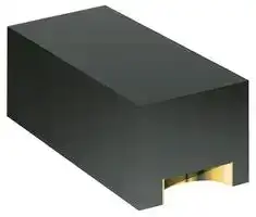
- Diode Case Style: 0603
- Diode Configuration: Single
- Forward Voltage Max: 1V
- Forward Surge Current: 4A
- Reverse Recovery Time: 4ns
- Average Forward Current: 150mA
- Operating Temperature Max: 125°C
- Repetitive Peak Reverse Voltage: 100V
| Delivery and price | |
|---|---|
| Units per pack | 20000 |
| Price | 0.043 € |
| Current stock | 10+ |
| Lead time | 30 days |
## **Features**

■ RoHS compliant*

■ Leadless 0603 (1608) chip

- High speed switching

## **Applications**

■ Cellular phones

■ PDAs

■ Desktop PCs and notebooks

■ Digital cameras

■ MP3 players

## **CD0603-S01575 Switching Chip Diode**

## ~~**General Information**~~

The markets of portable communications, computing and video equipment are challenging the semiconductor industry to develop increasingly smaller electronic components.

Bourns offers small-signal high-speed Switching Diodes for switching digital signal applications, in compact chip package 0603 size format, which offers PCB real estate savings and are considerably smaller than competitive parts. The Switching Diodes offer a Repetitive Peak Forward Current of 200 mA and a reverse voltage of 75 V. The diodes are RoHS compliant and are compatible with lead-free manufacturing processes, conforming to many industry and government regulations on lead-free components. Bourns[®] Chip Diodes conform to JEDEC standards, are easy to handle on standard pick and place equipment and their fl at confi guration minimizes roll away.

## ~~**Absolute Maximum Ratings (@ T**~~ **A** ~~**= 25 °C Unless Otherwise Noted)**~~

|**Parameter**|**Symbol**|**Value**|**Unit**|
|---|---|---|---|
|Repetitive Peak Reverse Voltage|VRRM|100|V|
|Reverse Voltage|VR|80|V|
|Average Forward Current|IF(AV)|100|mA|
|Repetitive Peak Forward Current|IFRM|225|mA|
|Non-repetitive Surge Forward Current<br>@t < 1 s<br>@t < 8.3 ms|IFSM|400<br>800|mA|
|Power Dissipation|PD|150|mW|
|Thermal Resistance Junction to Ambient Air|RƟJA|375|°C/W|
|Storage Temperature|TSTG|-55 to +150|°C|
|Operating Temperature|TJ|-55 to +150|°C|


## ~~**Electrical Characteristics (@ T**~~ **A** ~~**= 25 °C Unless Otherwise Noted)**~~

|**Parameter**|**Symbol**|**Value**|**Unit**|
|---|---|---|---|
|Forward Voltage (Max.)|VF|1.00 (If = 50 mA)<br>1.20 (If= 100 mA)|V|
|Capacitance Between Terminals (Max.)|CT|3<br>(Vr= 1 V, f = 1 MHz)|pF|
|Reverse Recovery Time (Max.)|trr|4<br>(IF= IR= 10 mA, RL= 50 ohms)|nS|
|Reverse Current (Max.)|IR|2.5<br>(VR = 70 V)|μA|


~~**How to Order**~~

**CD 0603  S  015  75** Common Code Chip Diode Package •  0603 Model **EMEA:** S = High-speed Switching Average Forward Current (Io) Code 015 = 150 mA _(Code x 1000 mA = Average Forward Current)_ ==)" Reverse Voltage (VR) Code 75 = 75 V

**Asia-Pacifi c:** Tel: +886-2 2562-4117 • Fax: +886-2 2562-4116 **EMEA:** Tel: +36 88 520 390 • Fax: +36 88 520 211

**The Americas:** Tel: +1-951 781-5500 • Fax: +1-951 781-5700 **www.bourns.com**

*RoHS Directive 2002/95/EC Jan. 27, 2003 including annex and RoHS Recast 2011/65/EU June 8, 2011. Specifi cations are subject to change without notice. The device characteristics and parameters in this data sheet can and do vary in different applications and actual device performance may vary over time. Users should verify actual device performance in their specifi c applications.

## **CD0603-S01575 Switching Chip Diode**

**==> picture [499 x 254] intentionally omitted <==**

**----- Start of picture text -----**<br>
Product Dimensions Recommended Pad Layout<br>1.55 ± 0.1 A<br>(0.061 ± .004)<br>0.80  ± 0.1<br>(0.031 ± .004)<br>D<br>B C<br>0.65 ± 0.1<br>(0.026 ± .004)<br>Dimensions<br>1.8 - 2.6<br>A<br>0.35 ± 0.1 (0.075 - 0.102)<br>(0.14 ± .004) 0.8<br>B<br>MM (0.031)<br>DIMENSIONS:<br>(INCHES) 0.5 - 0.9<br>C<br>(0.020 - 0.035)<br>0.8 - 1.0<br>D<br>(0.031 - 0.039)<br>**----- End of picture text -----**<br>


**Dimensions** 1.8 - 2.6 A (0.075 - 0.102) 0.8 B (0.031) 0.5 - 0.9 C (0.020 - 0.035) 0.8 - 1.0 D (0.031 - 0.039) MM DIMENSIONS: (INCHES)

~~**Physical Specif cations**~~ Case .......................................................0603 (1608) Molded plastic Terminals ..................... Solder plated, solderable per MIL-STD-750, Method 2026 Polarity.....................................................Indicated by cathode band Mounting Position ........................................................................Any

Specifi cations are subject to change without notice. The device characteristics and parameters in this data sheet can and do vary in different applications and actual device performance may vary over time. Users should verify actual device performance in their specifi c applications.

## **CD0603-S01575 Switching Chip Diode**

## ~~**Rating and Characteristic Curves: CD0603-S01575**~~

## ~~**Forward Characteristics**~~

**==> picture [231 x 200] intentionally omitted <==**

**----- Start of picture text -----**<br>
1000<br>100<br>10<br>25 °C<br>125 °C 85 °C -25 °C<br>1<br>0.0 0.2 0.4 0.6 0.8 1.0 1.2<br>Forward Voltage (Volts)<br>Forward Current (mAmps)<br>**----- End of picture text -----**<br>


## ~~**Derating Curve**~~

**==> picture [221 x 209] intentionally omitted <==**

**----- Start of picture text -----**<br>
120<br>Mounting on glass epoxy PCBs<br>100<br>80<br>60<br>40<br>20<br>0<br>0 25 50 75 100 125 150<br>Ambient Temperature (°C)<br>I0 Current (%)<br>**----- End of picture text -----**<br>


## ~~**Reverse Characteristics**~~

**==> picture [241 x 193] intentionally omitted <==**

**----- Start of picture text -----**<br>
100.0<br>10.0<br>125  ° C<br>1.0 85 °C<br>0.1<br>25 °C<br>0<br>0 10 20 30 40 50 60 70 80<br>Reverse Voltage (Volts)<br>Reverse Current (nA)<br>**----- End of picture text -----**<br>


## ~~**Capacitance Between Terminals**~~

**==> picture [227 x 211] intentionally omitted <==**

**----- Start of picture text -----**<br>
5.0<br>F = 100 MHz<br>Ta = 25 °C<br>4.0<br>3.0<br>2.0<br>1.0<br>0.0<br>0 2 4 6 8 10 12 14<br>Reverse Voltage (Volts)<br>Capacitance Between Terminals (pF)<br>**----- End of picture text -----**<br>


Specifi cations are subject to change without notice. The device characteristics and parameters in this data sheet can and do vary in different applications and actual device performance may vary over time. Users should verify actual device performance in their specifi c applications.

## **CD0603-S01575 Switching Chip Diode**

## ~~**Packaging Information**~~

The product is dispensed in tape and reel format (see diagram below).

P0 d P1 E T Index Hole F W . B ~~eocey~~ P A C ~~icine~~ Se Trailer Device Leader ~~_—— -— JL~~ ....... ....... ....... ....... End ....... ....... ....... ....... 10 pitches (min.) 10 pitches (min.) ~~|__| |_____.|~~

Direction of Feed

~~ee~~ **Item Symbol** ~~ee~~ **0603** 1.00 ± 0.10 Carrier Width A (0.039 ± 0.004) 1.70 ± 0.10 Carrier Length B ~~—ST~~ (0.067 ± 0.004) 1.00 ± 0.10 Carrier Depth C ~~eeee ee~~ (0.039 ± 0.004) 1.55 ± 0.10 Sprocket Hole d ~~eeeeee~~ (0.061 ± 0.004) ~~e~~ 178 Reel Outside Diameter D ~~eeee~~ (7.008) ~~ee~~ 60.0 Reel Inner Diameter D1 ~~eeee~~ (2.362)[MIN.] 13.0 ± 0.20 Feed Hole Diameter D2 ~~eeee ee~~ (0.512 ± 0.008) 1.75 ± 0.10 Sprocket Hole Position E ~~eeeeee~~ (0.069 ± 0.004) 3.50 ± 0.05 Punch Hole Position F ~~eeee ee~~ (0.138 ± 0.002) 4.00 ± 0.10 Punch Hole Pitch P ~~eeeeee~~ (0.157 ± 0.004) 4.00 ± 0.10 Sprocket Hole Pitch P0 ~~eeee ee~~ (0.157 ± 0.004) 2.00 ± 0.05 Embossment Center P1 ~~eeee~~ (0.079 ± 0.002) 0.20 ± 0.05 Overall Tape Thickness T ~~eeee ee~~ (0.008 ± 0.002) 8.00 ± 0.20 Tape Width W (0.315 ± 0.008) ~~ee ee~~ 13.5 Reel Width W1 ~~ee~~ (0.531)[MAX.] ~~es~~ Quantity per Reel -- 5,000

Start

120 ° D2 D1 D ~~3B O~~ . ~~| ~~~ W1 MM DIMENSIONS: (INCHES) ~~_~~

Devices are packed in accordance with EIA-481 standard and specifi cations shown here.

REV. 02/15

Specifi cations are subject to change without notice. The device characteristics and parameters in this data sheet can and do vary in different applications and actual device performance may vary over time. Users should verify actual device performance in their specifi c applications.
Updated at February 9, 2023
Bourns, Inc. is a globally recognized manufacturer of high-reliability electronic components, headquartered in Riverside, California. Renowned for its engineering excellence, the company delivers critical solutions across a diverse range of demanding markets, including automotive, industrial, consumer electronics, telecommunications, and medical equipment. The Bourns product portfolio is anchored by an industry-leading selection of passive components and circuit protection devices. The brand is particularly dominant in magnetic components, offering thousands of high-performance power inductors, alongside specialized RF and toroidal inductors engineered for optimized power management and signal integrity. Equally prominent is their comprehensive suite of circuit protection solutions. This robust lineup features a vast array of standard and resettable fuses, transient voltage suppressors (including TVS varistors and diodes), and gas discharge tubes (GDTs) designed to rigorously safeguard sensitive electronics against overvoltage and overcurrent faults. Beyond its core passives and protection technologies, Bourns manufactures highly effective EMC and RFI suppression components, such as common mode chokes and power line filters. The company's offering also extends into discrete semiconductors and power management, including Schottky diodes, fast recovery rectifiers, bridge rectifiers, and board-level transformers. This expansive breadth of quality components provides design engineers with a trusted foundation for developing resilient, efficient, and long-lasting electronic systems.
About Novapart
Novapart is a B2B electronic component broker specialising in stock shortages and cost reduction. We source hard-to-find parts and identify compliant alternatives across a catalogue of 410,000+ components from 500+ manufacturers.
Learn more →Stock Shortage Specialist
When a component is unavailable, discontinued or has an unacceptable lead time, we tap into our network of vetted European and Asian distributors to source what you need — without compromising on quality or traceability.
Request a quote →Compliant Alternatives
We identify pin-to-pin, electrically equivalent substitutes that meet the same certifications (RoHS, AEC-Q100, REACH) as your original specification — validated against datasheets, not just part numbers. Often at a lower cost.
BOM Analysis service →