
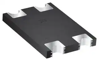


CD-DF410S
Bridge Rectifier, Single Phase, 1 kV, 4 A, SMD, 4 Pins, 950 mV
- Manufacturer: BOURNS
- Product type: Bridge Rectifier Diodes
- No. of Phases:Single Phase; Repetitive Reverse Voltage Vrrm Max:1kV; Forward Current If(AV):4A; Bridge Rectifier Case Style:SMD; Forward Voltage VF Max:950mV; No. of Pins:4Pins; Operat
- SVHC: Lead (04-Feb-2026)
- No. of Pins: 4Pins
- No. of Phases: Single Phase
- Product Range: CD-DF4xxS
- Forward Voltage Max: 950mV
- Forward Surge Current: 150A
- Average Forward Current: 4A
- Bridge Rectifier Mounting: Surface Mount
- Operating Temperature Max: 175°C
- Bridge Rectifier Case Style: SMD
- Repetitive Peak Reverse Voltage: 1kV
| Delivery and price | |
|---|---|
| Units per pack | 1500 |
| Price | 0.287 € |
| Current stock | 1000+ |
| Lead time | 30 days |
## **Features**

■ Working voltage 3.3 V ■ SMT - DFN package ■ Low capacitance - 4 pF ■ IEC 61000-4-2 (ESD) ■ IEC 61000-4-4 (EFT) ■ IEC 61000-4-5 (Surge)

Model CDDFN10-3304N is currently available, although not recommended for new designs. Model CDDFN10-3304NA is preferred.

## POURNS ~~Ei~~ **CDDFN10-3304N - TVS/Steering Diode Array**

## ~~**General Information**~~

The CDDFN10-3304N device provides ESD, EFT and Surge protection for high speed data ports meeting IEC 61000-4-2 (ESD), IEC 61000-4-4 (EFT) and IEC 61000-4-5 (Surge) requirements. The Transient Voltage Suppressor array, protecting up to 4 data lines, offers a Working Peak Voltage of 3.3 V.

The DFN-10 packaged device will mount directly onto the industry standard DFN-10 footprint. Bourns[®] Chip Diodes are easy to handle with standard pick and place equipment.

## ~~**Absolute Maximum Ratings,  T**~~ **A** ~~**= 25 °C (Unless Otherwise Noted)**~~

|**Parameter**|**Symbol**|**CDDFN10-3304N**|**Unit**|
|---|---|---|---|
|Peak Pulse Power (tp= 8/20 μs)(NOTE 1)|PPK|450|W|
|Peak Pulse Current (tp = 8/20 μs)<br>per IEC 61000-4-5|IPP|25|A|
|Storage Temperature|TSTG|-55 to +150|ºC|
|Operating Temperature|TOPR|-55 to +125|ºC|
|ESD Protection per IEC 61000-4-2<br>Contact Discharge<br>Air Discharge||30 max.<br>30 max.|kV<br>kV|
|EFT Protection per IEC 61000-4-4 @ 5/50 ns||40 min.|A|


Notes:

1. See Peak Pulse Power vs. Pulse Time.

~~**Electrical Characteristics (@ T**~~ **A** ~~**= 25 °C Unless Otherwise Noted)**~~

|~~a~~||~~(~~||||
|---|---|---|---|---|---|
|**Parameter**<br>~~(OD~~<br>~~a~~|**Symbol**<br>~~(OD~~|**Min.**<br>~~(OD~~<br>~~(~~|**Typ.**<br>~~(OD~~|**Max.**<br>~~(OD~~|**Unit**<br>~~(OD~~|
|Breakdown Voltage @ 1 mA<br>~~a~~|VBR|3.9<br>~~(~~|||V|
|Working Peak Voltage<br>~~ee~~<br>~~ee~~|VWM<br>~~ee~~<br>~~GO~~|~~ee~~<br>~~GO~~|~~ee~~<br>~~GO~~|3.3<br>~~ee~~|V<br>~~ee~~|
|Leakage Current1@ VWM<br>~~ee~~|ID<br>~~GO~~|~~GO~~|~~GO~~|1|μA|
|Clamping Voltage2@ IP= 5 A 8/20 μs<br>~~ee ~~<br>~~GG~~|VC<br> ~~GO~~<br>~~GG~~|~~GO~~<br>~~GG~~|~~GO~~<br>~~GG~~|15<br>~~GG~~|V<br>~~GG~~|
|Clamping Voltage2@ IP= 15 A 8/20 μs<br>~~GO~~|VC<br>~~GO~~|~~GO~~|~~GO~~|18<br>~~GO~~|V<br>~~GO~~|
|Clamping Voltage2@ IP= 20 A 8/20 μs<br>~~GO~~<br>~~GG~~|VC<br>~~GO~~<br>~~GG~~|~~GO~~<br>~~GG~~|~~GO~~<br>~~GG~~|20<br>~~GO~~<br>~~GG~~|V<br>~~GO~~<br>~~GG~~|
|Junction Capacitance2@ 0 V 1 MHz<br>~~Ge~~|CD<br>~~Ge~~|~~GO~~|4.0<br>~~GO~~|5.0<br>~~GO~~|pF|
|Junction Capacitance3@ 0 V 1 MHz<br>~~Ge~~<br>~~p~~|CIO<br>~~Ge~~<br>~~p~~|~~GO~~<br>~~pO~~|1.5<br>~~GO~~<br>~~O~~|~~GO~~<br>~~O~~|pF<br>~~O~~|


Note 1: Pin 5 to ground. Note 2: Pin 1,3,7 or 9 to ground. Note 3: Between Pin 1,3,7 and 9.

**WARNING  Cancer and Reproductive Harm -** www.P65Warnings.ca.gov

*RoHS Directive 2015/863, Mar 31, 2015 and Annex.

Specifications are subject to change without notice. Users should verify actual device performance in their specific applications. The products described herein and this document are subject to specific legal disclaimers as set forth on the last page of this document, and at www.bourns.com/docs/legal/disclaimer.pdf.

## **CDDFN10-3304N - TVS/Steering Diode Array**

## ~~**Rating & Characteristic Curves**~~

## ~~**Peak Pulse Power vs. Pulse Time**~~

**==> picture [243 x 523] intentionally omitted <==**

**----- Start of picture text -----**<br>
10,000<br>1000 450 W, 8/20 µs Waveform<br>100<br>10<br>0.01 1 10 100 1,000 10,000<br>td – Pulse Duration (µs)<br>Clamping Voltage vs Peak Pulse Current<br>22<br>20<br>18 Any I/O Pin to GND<br>16<br>14<br>12<br>10<br>8<br>6 Waveform<br>4 Parameters:<br>tr = 8 µs<br>2 td = 20 µs<br>0<br>0 5 10 15 20 25<br>Peak Pulse Current (A)<br>Typical Voltage vs. Capacitance<br>4.5<br>4.0 Any I/O Pin to GND<br>3.5<br>3.0<br>2.5<br>2.0<br>1.5<br>1.0<br>VDD = Floating, GND = 0 V,<br>0.5<br>f = 1 MHz, T = 25 °C<br>0.0<br>0.0 0.5 1.0 1.5 2.0 2.5 3.0 3.5<br>Input Voltage (V)<br> – Peak Pulse  (W)<br>PP<br>P<br>Clamping Voltage (V)<br>Input Capacitance  (pF)<br>**----- End of picture text -----**<br>


## ~~**Pulse Waveform**~~

**==> picture [224 x 527] intentionally omitted <==**

**----- Start of picture text -----**<br>
120<br>Test Waveform Parameters<br>100 tt tt = 8 µs<br>td = 20 µs<br>80<br>e [t]<br>60<br>40<br>td = t|IPP/2<br>20<br>0<br>0 5 10 15 20 25 30<br>t – Time (µs)<br>Clamping Voltage vs Peak Pulse Current<br>24<br>22<br>20 Any I/O Pin to Another I/O Pin<br>18<br>16<br>14<br>12<br>10<br>8<br>6 Waveform<br>Parameters:<br>4<br>tr = 8 µs<br>2 td = 20 µs<br>0<br>0 5 10 15 20 25<br>Peak Pulse Current (A)<br>Power Derating Curve<br>100<br>Peak Pulse Power<br>8/20 µs<br>80<br>60<br>40<br>20<br>Average Power<br>0<br>0 25 50 75 100 125 150<br>TL - Lead Temperature (°C)<br>)PP<br> – Peak Pulse Current (% of I<br>IPP<br>Clamping Voltage (V)<br>% of Rated Power<br>**----- End of picture text -----**<br>


## ~~**Clamping Voltage vs Peak Pulse Current**~~

~~**Power Derating Curve**~~

Specifications are subject to change without notice. Users should verify actual device performance in their specific applications. The products described herein and this document are subject to specific disclaimers as set forth on the last page of this document, and at www.bourns.com/legal/disclaimer.pdf.

## **CDDFN10-3304N - TVS/Steering Diode Array**

## ~~**Product Dimensions**~~

This is a molded DFN10 package with lead free Nickel-PaladiumGold (Ni/Pd/Au) on the lead frame. It has a flammability rating of UL 94V-0.

**==> picture [188 x 357] intentionally omitted <==**

**----- Start of picture text -----**<br>
2.45 - 2.55<br>(0.096 - 0.100)<br>2.45 - 2.55<br>(0.096 - 0.100)<br>PIN 1<br>INDICATOR<br>0.50 - 0.60<br>(0.020 - 0.024)<br>0.152<br>(0.006)<br>0.20 - 0.30 0.50<br>(0.008 - 0.012) (0.020)<br>PIN 1<br>0.2<br>R (.008) 1.15 - 1.25<br>(0.045 - 0.049)<br>1.85 - 1.95 0.35 - 0.45<br>(0.073 - 0.077) (0.014 - 0.018)<br>2.10 - 2.20<br>(0.083 - 0.087)<br>**----- End of picture text -----**<br>


## ~~**How to Order**~~

## **CD DFN10 - 33  04  N**

Common Diode Chip Diode Package DFN10 = DFN-10 Package Working Peak Voltage 33 = 3.3 VRWM (Volts) Number of Lines 04 = 4 Data Lines

Suffix N = Low Capacitance

## ~~**Recommended Footprint**~~

**==> picture [185 x 135] intentionally omitted <==**

**----- Start of picture text -----**<br>
0.50 0.30<br>(.020) (.012)<br>3.15<br>(.124)<br>1.26 2.50<br>1.85 (.050) (.100)<br>(.073)<br>MM<br>DIMENSIONS:<br>0.65 2.05 (INCHES)<br>(.026) (.081)<br>**----- End of picture text -----**<br>


## ~~**Typical Part Marking**~~

|334<br>YWLLL<br>DEVICE CODE:<br>334 = CDDFN10-3304N<br>LOT<br>TRACEABILITY<br>CODE<br>DATE CODE<br>YEAR CODE:<br>5 = 2015<br>6 = 2016<br>WEEK CODE:<br>4 = WEEK 15 to WEEK 21<br>5 = WEEK 22 to WEEK 28|**Week**<br>**Code**|**Duration**|
|---|---|---|
||2|Week 1~Week 7|
||3|Week 8~Week 14|
||4|Week 15~Week 21|
||5|Week 22~Week 28|
||6|Week 29~Week 35|
||7|Week 36~Week 42|
||8|Week 43~Week 49|
||9|Week 50~Week 52|


## ~~**Pin Out**~~

**==> picture [229 x 183] intentionally omitted <==**

**----- Start of picture text -----**<br>
Pin Function<br>1 I/O<br>2 N.C.<br>CH1 1 10 NC<br>3 I/O<br>NC 2 9 CH2 4 N.C.<br>CH3 3 GND 8 NC 5 VCC<br>(CENTER TAB)<br>NC 4 7 CH4 6 N.C.<br>7 I/O<br>VDD 5 6 NC<br>8 N.C.<br>TOP VIEW<br>9 I/O<br>10 N.C.<br>CENTER<br>GROUND<br>TAB<br>**----- End of picture text -----**<br>


Specifications are subject to change without notice. Users should verify actual device performance in their specific applications. The products described herein and this document are subject to specific disclaimers as set forth on the last page of this document, and at www.bourns.com/legal/disclaimer.pdf.

## **CDDFN10-3304N - TVS/Steering Diode Array**

## ~~**Packaging Information**~~

The product will be dispensed in tape and reel format (see diagram below).

**==> picture [204 x 160] intentionally omitted <==**

**----- Start of picture text -----**<br>
120 °<br>D2<br>D1 D<br>W1<br>MM<br>DIMENSIONS:<br>(INCHES)<br>**----- End of picture text -----**<br>


**==> picture [277 x 191] intentionally omitted <==**

**----- Start of picture text -----**<br>
P0<br>P1 E T<br>d Index Hole<br>Pin 1<br>Location<br>F<br>W<br>B<br>P A C<br>Trailer Device Leader<br>....... ....... ....... .......<br>End ....... ....... ....... ....... Start<br>10 pitches (min.) 10 pitches (min.)<br>Direction of Feed<br>**----- End of picture text -----**<br>


Devices are packed in accordance with EIA standard RS-481-A.

|**Item**|**Symbol**||||**DFN-10**|**DFN-10**|
|---|---|---|---|---|---|---|
|Carrier Width|A||||2.80 ± 0.10<br>(0.110 ± 0.004)||
|Carrier Length|B||||2.85±0.10<br>(0.112 ± 0.004)||
|Carrier Depth|C||||1.00 ± 0.05<br>(0.039 ± 0.002)||
|Sprocket Hole|d||||||
|Reel Outside Diameter|D||||180 ± 3<br>(7.087 ± 0.118)||
|Reel Inner Diameter|D1||||<br>(|50.0<br>1.969)MIN.|
|Feed Hole Diameter|D2||||||
|Sprocket Hole Position|E||||1.75 ± 0.10<br>(0.069 ± 0.004)||
|Punch Hole Position|F||||5.50 ± 0.05<br>(0.217 ± 0.002)||
|Punch Hole Pitch|P||||4.00 ± 0.10<br>(0.157 ± 0.004)||
|Sprocket Hole Pitch|P0||||4.00 ± 0.10<br>(0.157 ± 0.004)||
|Embossment Center|P1||||2.00 ± 0.05<br>(0.079 ± 0.002)||
|Overall Tape Thickness|T||||<br>(|0.60<br>0.024)MAX.|
|Tape Width|W||||<br>(|12.3<br>0.484)MAX.|
|Reel Width|W1||||<br>(|18.4<br>0.724)MAX.|
|Quantity per Reel|--|||||3000|


## **Asia-Pacific:**

Tel: +886-2 2562-4117 Email: asiacus@bourns.com **Europe:**

Tel: +36 88 885 877 Email: eurocus@bourns.com **The Americas:** Tel: +1-951 781-5500 Email: americus@bourns.com **www.bourns.com**

## REV. 08/19

Specifications are subject to change without notice. Users should verify actual device performance in their specific applications. The products described herein and this document are subject to specific legal disclaimers as set forth on the last page of this document, and at www.bourns.com/docs/legal/disclaimer.pdf.

®

## **Legal Disclaimer Notice**

This legal disclaimer applies to purchasers and users of Bourns[®] products manufactured by or on behalf of Bourns, Inc. and

Unless otherwise expressly indicated in writing, Bourns[®] products and data sheets relating thereto are subject to change

and complete before placing orders for Bourns[®] products.

The characteristics and parameters of a Bourns[®] product set forth in its data sheet are based on laboratory conditions, and statements regarding the suitability of products for certain types of applications are based on Bourns’ knowledge of typical requirements in generic applications.  The characteristics and parameters of a Bourns[®] product in a user application may

® product with other components ®

the actual performance of the Bourns[®]

® product as meeting the requirements of a particular industry

failure of an individual Bourns ® product to meet the requirements of such industry standard or particular qualification. Users of Bourns[®] products are responsible for ensuring compliance with safety-related requirements and standards applicable to

Bourns[®]

on a case-by-case basis, use of any Bourns[®]

®

®

®

Bourns[®]

® standard products that are suitable for use in aircraft “Applications.” Unless expressly and specifically ® standard

the user’s sole risk.

and the user for which such Bourns[®] custom and the user regarding the use and level of also apply to such Bourns[®] custom products.

® custom products shall be negotiated on a case-by-case basis by Bourns are specially designed. Absent a written agreement between Bourns testing, the above provisions applicable to Bourns ® standard products shall

Users shall not sell, transfer, export or re-export any Bourns[®]

Bourns[®]

regulations. Further, Bourns ® products and Bourns technology and technical data may not under any circumstance be exported or re-exported to countries subject to international sanctions or embargoes.  Bourns[®] products may not, without

_bilingual versions are available at:_

_Web Page: http://www.bourns.com/legal/disclaimers-terms-and-policies PDF: http://www.bourns.com/docs/Legal/disclaimer.pdf_
Updated at June 4, 2026
Bourns, Inc. is a globally recognized manufacturer of high-reliability electronic components, headquartered in Riverside, California. Renowned for its engineering excellence, the company delivers critical solutions across a diverse range of demanding markets, including automotive, industrial, consumer electronics, telecommunications, and medical equipment. The Bourns product portfolio is anchored by an industry-leading selection of passive components and circuit protection devices. The brand is particularly dominant in magnetic components, offering thousands of high-performance power inductors, alongside specialized RF and toroidal inductors engineered for optimized power management and signal integrity. Equally prominent is their comprehensive suite of circuit protection solutions. This robust lineup features a vast array of standard and resettable fuses, transient voltage suppressors (including TVS varistors and diodes), and gas discharge tubes (GDTs) designed to rigorously safeguard sensitive electronics against overvoltage and overcurrent faults. Beyond its core passives and protection technologies, Bourns manufactures highly effective EMC and RFI suppression components, such as common mode chokes and power line filters. The company's offering also extends into discrete semiconductors and power management, including Schottky diodes, fast recovery rectifiers, bridge rectifiers, and board-level transformers. This expansive breadth of quality components provides design engineers with a trusted foundation for developing resilient, efficient, and long-lasting electronic systems.
About Novapart
Novapart is a B2B electronic component broker specialising in stock shortages and cost reduction. We source hard-to-find parts and identify compliant alternatives across a catalogue of 410,000+ components from 500+ manufacturers.
Learn more →Stock Shortage Specialist
When a component is unavailable, discontinued or has an unacceptable lead time, we tap into our network of vetted European and Asian distributors to source what you need — without compromising on quality or traceability.
Request a quote →Compliant Alternatives
We identify pin-to-pin, electrically equivalent substitutes that meet the same certifications (RoHS, AEC-Q100, REACH) as your original specification — validated against datasheets, not just part numbers. Often at a lower cost.
BOM Analysis service →