
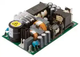


CCB200PS15
AC/DC Open Frame Power Supply (PSU), ITE & Medical, 1 Output, 200 W, 80V AC to 264V AC
- Manufacturer: XP POWER
- Product type: AC / DC Open Frame Power Supplies
- No. of Outputs:1 Output; Power Rating (Covection Cooling):200W; Power Rating (Forced Cooling):-; Input Voltage VAC:80V AC to 264V AC; Power Supply Output Type:Adjustable, Fixed;
- SVHC: No SVHC (15-Jan-2018)
- Product Range: CCB200 Series
- No. of Outputs: 1 Output
- Output Power Max: 200W
- Input Voltage VAC: 80V AC to 264V AC
- Input Voltage AC Max: 264V
- Input Voltage AC Min: 80V
- Power Supply Output Type: Adjustable, Fixed
- Output Current - Output 1: 13.3A
- Output Current - Output 2: -
- Output Current - Output 3: -
- Output Current - Output 4: -
- Output Voltage - Output 1: 15VDC
- Output Voltage - Output 2: -
- Output Voltage - Output 3: -
- Output Voltage - Output 4: -
- Power Supply Applications: ITE & Medical
- Power Rating (Forced Cooling): -
- Power Rating (Convection Cooling): 200W
| Delivery and price | |
|---|---|
| Units per pack | 10 |
| Price | 136.14 € |
| Current stock | 10+ |
| Lead time | 30 days |
**200/250 Watts**

xppower.com

## **CCB200/250 Series**

- 200 & 250 W Convection Cooled

- Very Low Heat Loss

- +70 °C Full Power Operation (CCB200)

- Very High Efficiency up to 95%

- 5 V Standby, Inhibit & Power Fail Signals

- IT & Medical (BF) Safety Approvals

- 3 Year Warranty

## ~~**Specification**~~

## **Input**

- Input Voltage • See derating curve Input Frequency • 47-63 Hz Input Current • 1.8/2.4 A typical at 115 VAC, full load (CCB200/250) 0.9/1.2 A typical at 230 VAC, full load (CCB200/250)

- Inrush Current • 30 A typical at 230 VAC, cold start at 25 °C Power Factor • >0.9 Earth Leakage Current • 250 μ A max at 264 VAC/60 Hz No Load Input Power • <0.5 W when inhibit used (CCB200) Patient Leakage Current • 100 μ A max, 264 VAC 60 Hz Input Protection • Internal T5.0 A/250 V fuse in line and neutral

- **Output put ut** Output Voltage • 12-48 VDC (see tables) Output Voltage Trim • ±3% CCB250, ±5% CCB200 (See Mechanical Details)

- Initial Set Accuracy • ±0.5% V1, ±5% V2 Minimum Load • No minimum load required Start Up Delay • 1 s typical Start Up Rise Time • 0.5 s typical Hold Up Time • 16/20 ms min at 90 VAC (CCB250/200) Drift • ±0.2% after 20 min warm up Line Regulation • ±0.5% max Load Regulation • ±1% V1, ±5% V2 Over/Undershoot • 5% max Transient Response • 4% max. deviation, recovery to within 1% in 500 μ s for a 50-75-50% load change

- Ripple & Noise • 1% pk-pk, 20 MHz bandwidth Overvoltage Protection • 115-140% Vnom, recycle input to reset (V1 only)

- Overload Protection • 125-165% Inom V1 (CCB250), 110 - 150% Inom V1 (CCB200)

- Short Circuit Protection • Continuous trip and restart (hiccup mode) Temperature • 0.05%/°C Coefficient Remote On/Off • Uncommitted isolated optocoupler diode, (Inhibit/Enable) powered diode inhibits V1

## **Output put ut**

- Efficiency • Up to 95% Isolation • 4000 VAC Input to Output 2 x MOPP, 1500 VAC Input to Ground 1 x MOPP, 1500 VAC Output to Ground 1 x MOPP

- Switching Frequency • See longform datasheet Signals • Power Fail Inhibit, 5 V Standby

- MTBF • 369/230 kHrs to MIL-HDBK-217F at 25 °C, GB (CCB250/200)

## **Environmental**

- Operating Temperature • See derating curve & longform datasheet Cooling • Convection cooled Operating Humidity • 95% RH, non-condensing Storage Temperature • -40 °C to +85 °C Operating Altitude • 3048 m for CCB250, 5000 m for CCB200 Shock • ±3 x 30g shocks in each plane, total 18 shocks. 30g = 11ms (±0.5 ms), half sine, conforms to EN60068-2-27 & EN60068-2-47

- Vibration • Single axis 10 - 500 Hz at 2g sweep and endurance at resonance in all 3 planes. Conforms to EN60068-2-6

## **EMC & Safety**

|**EMC & Safetyy**||
|---|---|
|Low Voltage PSU EMC|• EN61204-3, high severity level|
|Emissions|• EN55011/32 level B conducted|
||EN55011/32 level A radiated,|
||See longform datasheet for level A|
|Harmonic Currents|• EN61000-3-2, class A, >140w class C|
|Voltage Flicker|• EN61000-3-3|
|Radiated Immunity|• EN61000-4-3, level 3 Perf Criteria A|
|EFT/Burst|• EN61000-4-4, level 3 Perf Criteria A|
|Surge|• EN61000-4-5, installation class 3|
||Perf Criteria A|
|Conducted Immunity|• EN61000-4-6, level 3 Perf Criteria A|
|Dips & Interruptions|• EN61000-4-11 , 30% 10 ms, 60% 100 ms,|
||100% 5000 ms, Perf Criteria A, B, B ,|
|Safety Approvals|EN60601-1-2, 30% 500 ms, 60% 100 ms,<br>100% 10 ms, 100% 5000 ms, Perf Criteria<br>A, A, A, B - 230 VAC. Consult longform<br>datasheet for 115 V operation.<br>• IEC60950-1 & IEC62368-1 CB report,<br>UL62368-1, EN62368-1,|
||IEC60601-1 CB report, UL60601-1,|
||EN60601-1,EN60601-1, ANSI/AAMI|
||ES60601-1, CSA22.2 No.60601-1 per cUL|
||BF Rated, Including Risk Management,|
||CE & UKCA meets all applicable directives|
||& legislation.|


**General**

**CCB200**

## ~~**Models and Ratings**~~

|Output Power|Output Voltage V1<br>Max Output Current V1|Max Output Current V1<br>5 V Standby (Optional)|Model Number|
|---|---|---|---|
|200 W|12.0 V<br>16.7 A|16.7 A<br>5 V/0.5 A|CCB200PS12|
|200 W|15.0 V<br>13.3 A|13.3 A<br>5 V/0.5 A|CCB200PS15|
|200 W|24.0 V|8.3 A<br>5 V/0.5 A|CCB200PS24|
|200 W|28.0 V|7.1 A<br>5 V/0.5 A|CCB200PS28|
|200 W|48.0 V|4.2 A<br>5 V/0.5 A|CCB200PS48|
|200 W|56.0 V|3.6 A<br>5 V/0.5 A|CCB200PS56|


## ~~**Notes**~~

_1. For covered version add suffix -C to model number e.g. CCB200PS12-C_

2. Add suffix -A for 5 V standby option, or -AC for standby and cover options combined.

## ~~**Mechanical Details**~~

**==> picture [418 x 553] intentionally omitted <==**

**----- Start of picture text -----**<br>
5.00 ±0.02 (127.0 ±0.5) (0.307.50)<br>ø0.14 (3.5)<br>thru in 4 positions<br>Output<br>ai e 3 L3 K JS | VoltageControl<br>A<br>C64<br>2.55 C53 -VE<br>(64.77) 0.92<br>(23.48) 1<br>—_ 2 neee. 1.49 Zam +VE<br>T1 (37.91)<br>Output Terminals<br>M4 Screws in<br>0.22 4.55 2 positions.<br>(5.71)0.22 (5.71) (115.57) (20.2)0.80 Torque to 8lbs-in (90 Ncm) max.<br>Pin 2 Pin 1<br>ae.<br>1.43 ±0.04<br>(36.32 ±1.0) Pin 10 Pin 9<br>Mounting holes marked with Detail A<br>must be connected to safety earth. ® PM | | ) | 10 way JST B10B-PHDSSSignals Connector CON4 —<br>0.13<br>(3.5)<br>ø0.14 (3.5)<br>thru in 4 positions 5.00 ±0.02 (127.0 ±0.51) 0.30 (7.5)<br>A<br>L3<br>A Output<br>C64 C53 under  Voltage<br>standby board Control<br>— (64.7)2.55 se Ee® Fa kt B -VE<br>Standby<br>Board<br>T1 3.00 ±0.02(Option -A) 37.8)1.49 +VE<br>(76.2 ±0.51)<br>Output<br>Terminals<br>M4 Screws in<br>(5.71)0.22 (23.4)0.92 (5.71)0.22 4.55 (115.5) (20.2)0.80 Pin 4 2 positions.Torque to 8lbs-in<br>Pin 3 (90 Ncm) max.<br>Pin 2<br>Pin 1<br>1.43 ±0.04<br>(36.32 ±1.0) Detail B<br>Standby Board O/P<br>Connector Cons<br>JST S48-PH-K-S<br>0.13<br>(3.5)<br>Mates with JST PHR-4 housing<br>and JST SPH-002T-P0.5L crimp<br>terminals<br>In put Connector CON 1 Output Connector CON 3 Signals Connector CON 4 Standby Output<br>1 Line 1 +VE 1 Power Fail (Emitter) (Option -A)<br>2 Neutral 2 -VE 2 Power Fail (Collector) 1 +5 V<br>3 Inhibit (Cathode) 2 +5 V<br>Mates with Molex housing   4 Inhibit (Anode) 3 0 V<br>09-50-1031 and Molex series  5 N/C 4 0 V<br>5194 crimp terminals.  6 N/C<br>7 - VE Sense<br>8 - VE Sense<br>9 +VE Sense<br>10 +VE Sense<br>Mates with JST PHDR-10VS<br>housing and JST SPHD-001T-<br>P0.5 crimp terminals<br>3.00 ±0.02 (76.2 ±0.5)<br>**----- End of picture text -----**<br>


## **CCB200PSxx Models**

## **CCB200PSxx-A Models**

## ~~**Notes**~~

1. All dimensions in inches (mm).

3. Weight: 0.88 lb (400 g) approx

2. Tolerance .xx = ±0.02 (0.50); .xxx = ±0.01 (0.25)

**CCB200**

## ~~**Mechanical Details**~~

## **CCB200PSxx-C Models**

**==> picture [496 x 621] intentionally omitted <==**

**----- Start of picture text -----**<br>
M3 Mounting Holes<br>in 2 positions<br>0.39 4.72 (120.0)<br>(9.85) é/ Pin 2 Di Az) Pin 1<br>Pin 10 5} Pin 9<br>0.93<br>(23.7) Signals Connector CON4Detail A<br>10 way JST B10B-PHDSS<br>1.75 (44.4) - 5.50 ±0.02 (139.7 ±0.5) — — 0.59 (15.0)<br>Con 4<br>TI Si A : oy a5 Output Voltage Control<br>| [Sota] ! i Con 3<br>1 | eeSoe ere) 3.48 ±0.02 (88.5 ±0.5) LoetT os | -VE Output Terminals<br>Con 1 [im= —— 2 | ee (43.9)1.73 Jr M4 Screws in 2 positions<br>+VE torque to 8 lbs<br>mcs | oaet e oes 1.03 Pelle (90 cNm) max.<br>(26.1)<br>La:—_ ab a tap e oS e a [ED] a ©l Con 2<br>0.39 4.72 (120.0)<br>(9.85) = [ae]<br>|<br>M3 mounting holes in 4 positions<br>o maximum penetration by screw to be3.0 mm from bottom face of cover In put Connector CON 1<br>: 1 Line<br>2 Neutral<br>1.97<br>(50.0) Mates with Molex housing<br>09-50-1031 and Molex<br>series 5194 crimp terminals.<br>Output Connector<br>0.7 Con 2, +VE<br>(19.3) Con 3, -VE<br>Signals Connector CON 4<br>M3 Mounting Holes 1 Power Fail (Emitter)<br>0.39 4.72 (120.0) in 2 positions 2 Power Fail (Collector)<br>(9.85) Pin 2 Pin 1 3 Inhibit (Cathode)<br>4 Inhibit (Anode)<br>(23.7)0.93 d/ Pin 1010 way JST B10B-PHDSSSignals Connector CON4 WJN izc Detail A tfees } Pin 9 5678 - VE Sense- VE SenseN/CN/C<br>9 +VE Sense<br>— 1.75 (44.4) [to] 5.50 ±0.02 (139.7 ±0.5) E 0.59 (15.0) 10 +VE Sense<br>Con 4<br>A : Hq Output Voltage Control Mates with JST PHDR-<br>TI | SieS68 r z 10VS housing and JST<br>Con 3 SPHD-001T-P0.5 crimp<br>1 3.48 ±0.02 (88.5 ±0.5) ha B -VE Output Terminals  terminals<br>Con 1 oO=oi ———— 2 | a ee e e (43.9)1.73 iz | +VE SS M4 Screws in 2 positionstorque to 8 lbs (90 cNm) max. Standby Output (Option -A)<br>ula | eos [e] [a][e] = (26.1)1.03 oR; 1 +5 V<br>| [a][|] cages e eeeters)42 aFilED:a Ic] Con 2 2 +5 V<br>0.39 4.72 (120.0) 3 0 V<br>(9.85) = [a] 4 0 V<br>O} M3 mounting holes in 4 positions _—<br>° maximum penetration by screw to be3.0 mm from bottom face of cover Mates with JST PHR-4<br>P<br>housing and JST<br>SPH-002T-P0.5L crimp<br>1.97<br>(50.0) terminals<br>° 2<br>0.7<br>(19.3)<br>**----- End of picture text -----**<br>


**==> picture [89 x 55] intentionally omitted <==**

**----- Start of picture text -----**<br>
In put Connector CON 1<br>1 Line<br>2 Neutral<br>Mates with Molex housing<br>09-50-1031 and Molex<br>series 5194 crimp terminals.<br>**----- End of picture text -----**<br>


## **CCB200PSxx-AC Models**

## ~~**Notes**~~

1. All dimensions in inches (mm). 2. Tolerance .xx = ±0.02 (0.50); .xxx = ±0.01 (0.25)

**==> picture [103 x 7] intentionally omitted <==**

**----- Start of picture text -----**<br>
3. Weight: 1.36 lb (618 g) approx<br>**----- End of picture text -----**<br>


**CCB250**

## ~~**Models and Ratings**~~

|Output Power|Output Power|Output Voltage V1<br>Nominal|Output Current V1|Standby Supply V2|Standby Supply V2<br>Model Number|
|---|---|---|---|---|---|
|Nominal|Nominal<br>Peak(1)||Nominal<br>Peak(1)|||
|250 W|250 W<br>300 W|12.0 V<br>20.8 A|20.8 A<br>25.00 A|5.0 V/0.5 A|CCB250PS12|
|250 W|250 W<br>300 W|15.0 V<br>16.7 A|16.7 A<br>20.00 A|5.0 V/0.5 A|CCB250PS15|
|250 W|250 W<br>300 W|24.0 V<br>10.4 A|10.4 A<br>12.50 A|5.0 V/0.5 A|CCB250PS24|
|250 W|250 W<br>300 W|28.0 V<br>8.9 A|8.9 A<br>10.70 A|5.0 V/0.5 A|CCB250PS28|
|250 W|250 W<br>300 W|36.0 V<br>6.9 A|6.9 A<br>8.30 A|5.0 V/0.5 A|CCB250PS36|
|250 W|250 W<br>300 W|48.0 V<br>5.2 A|5.2 A<br>6.25 A|5.0 V/0.5 A|CCB250PS48|


## ~~**Notes**~~

_1. Peak duration is 500ms max, average power must not exceed 250 W._

## ~~**Mechanical Details**~~

**==> picture [515 x 232] intentionally omitted <==**

**----- Start of picture text -----**<br>
6.00 (152.4)<br>0.24<br>(6.1)<br>| _ 4 Output<br>Signal Connector* Voltage<br>Adjustment<br>ø 3.5 L2<br>through<br>3) | 8 4 places fa Ea oa, a iL  tole -VE<br>CON 3<br>(94.6)3.73 C12 101.6(4.0) 2.60 +VE<br>Output  (66.3)<br>aU ! I og og gon a | Lie Moy = connectors 'eaiee<br>CON 4 NL allow connectionsfrom either  (50.4)1.98 Output TerminalsM4 Screws in 2 positions<br>0.74 E top or side torque to 8 lbs-in<br>(19.0) (90 cNm) max<br>©<br>0.14  C21<br>(3.5) 0.14  5.73 (145.42)<br>(3.5) *Signal Connector<br>BO Oo Pin 2 > all Pin 1 CON 1 10-way<br>JST-BI0B-PHDSS<br>Mating Half - p/n<br>o p = = H —— q q \¥ 38.1 ao JST PHDR-10VS,<br>Mounting holes married with (1.5) Pin 10 Pin 9 Contact- 26-22 AWG<br>must be connected to safety earth. p/n JST SPHD-001T-P0.5<br>**----- End of picture text -----**<br>


**==> picture [302 x 110] intentionally omitted <==**

**----- Start of picture text -----**<br>
Signals Connector CON 1 Output Connector CON 3 In put Connector CON 4<br>1 5 V Standby Return 1 +VE 1 Line<br>2 -VE 2 Neutral<br>2 5 V Standby<br>3 Earth<br>3 5 V Standby Return<br>4 5 V Standby Mates with Molex housing<br>5 5 V Standby Return 09-50-3051 and Molex series<br>6 5 V Standby 2478 crimp terminals.<br>7 Power Fail (Collector)<br>8 Power Fail (Emitter)<br>9 Remote On / Off (Cathode)<br>10 Remote On / Off (Anode)<br>**----- End of picture text -----**<br>


## ~~**Notes**~~

3. Weight 1.7 lb (780 g) approx

1. All dimensions in inches (mm). 2. Tolerance .xx = ±0.02 (0.50); .xxx = ±0.01 (0.25)

**CCB**

## ~~**Mechanical Details**~~

## ~~**Signals - CCB200**~~

**==> picture [500 x 544] intentionally omitted <==**

**----- Start of picture text -----**<br>
Power Fail Inhibit (High) Inhibit (Low)<br>5 V 5 V<br>POWER SUPPLY<br>POWER SUPPLY POWER SUPPLY<br>8V Max 3 mA Pin 2 CON 4Power Fail 5 mA    8 V Max 1K<br>Collector  Inhibit Hi  8 V Max<br>Pin 4 CON 4 Inhibit Hi<br>Transistor On: Input & Output Not OK Pin 4<br>Power Fail Transistor Off: Input & Output OK CON 4<br>Emitter<br>Pin 1 CON 4 Inhibit Lo Inhibit Lo<br>Pin 3 CON 4 5 mA Pin 3 CON 4<br>oo Signal Connector ! Pin 7 CON 4VI RTN ! Signal Connector | Pin 7 CON 4VI RTN Signal Connector<br>Signals Notes & Conditions<br>Power Fail Uncomitted opto isolated transistor, normally off when AC is good (see fig.5)<br>Provides 5 - 15ms warning of loss of output from AC failure<br>Remote On/Off (Inhibit/Enable) Uncommited isolated optocoupler diode, powered diode inhibits the supply (see fig.6 & 7)<br>5 V Standby (Optional -A) 5 V/0.5 A Supply, always present when AC applied<br>Input Voltage & Temperature Derating - CCB200<br>220 200<br>193 Open Frame Convection<br>200 182<br>Standby Open Frame (-A)<br>180 150<br>144.75 Covered Convection (-C)<br>160 136.5<br>Standby Covered<br>140 100 Convection (-AC)<br>120<br>0<br>== -20 0 +50 +70 +85<br>80 85 90 264 300<br>Input Voltage (VAC) Ambient Temperature (ºC)<br>Signals - CCB250<br>Power Fail Inhibit (High) Inhibit (Low)<br>POWER SUPPLY POWER SUPPLY<br>Pin 2, 4 & 6CON 15 V Standby   2K2 5 V Standby 2, 4 & 6 CON 1 Pin 2, 4 & 6 5 V Standby  POWER SUPPLY<br>CON 1<br>Oo 5 mA    8 V Max oe pe<br>8V Max 3 mA Pin 7 CON 1<br>Power FailCollector  Pin 10 CON 1Inhibit Hi  Inhibit Hi 8 V Max<br>Pin 10<br>Power FailEmitter Transistor Off (>4.5 V): Input & Output OKTransistor On (<0.8 V): Input & Output Not OK Inhibit Lo Inhibit LoCON 1<br>Pin 8 CON 1 Pin 9 CON 1 1K 5 mA Pin 9 CH 1 1K<br>5 V Standby RtnPin 1, 3 & 5CON 1 Logic GND Pin1, 3 & 5 CON 1 Logic GND Pin 1, 3 & 5 CON 1<br>Signal Connector Signal Connector Signal Connector<br>Signals Notes & Conditions<br>Power Fail Uncommitted opto isolated transistor, normally off when AC is good<br>Provides  ≥  5 ms (typically 20-30 ms) warning of loss of output from AC failure<br>Remote On/Off (Inhibit/Enable) Uncommitted isolated optocoupler diode, powered diode inhibits the supply<br>Standby Supply V2 Isolated 5 V/0.5 A supply, always present when AC supplied.<br>Output Power (W)<br>Output Power (Watts)<br>5 Seconds Maximum<br>**----- End of picture text -----**<br>


## ~~**Input Voltage & Temperature Derating - CCB200**~~

## ~~**Input Voltage & Temperature Derating - CCB250**~~

**==> picture [422 x 83] intentionally omitted <==**

**----- Start of picture text -----**<br>
300 300<br>Peak Power Availability Peak Power Availability<br>250 250<br>200 200<br>150 a ee ee 150 Qs<br>100 ae 100<br>50 eeee 50<br>ee ee 0 _t | |<br>80 85 90 264 275 -20 -10 0 10 40 50 60 70<br>Input Voltage (VAC) Ambient Temperature (°C)<br>Output Power (W)<br>Output Power (W)<br>**----- End of picture text -----**<br>


09 June 2022
Updated at June 8, 2026
XP Power is a globally recognized leader in the design and manufacture of critical power solutions for the electronics industry. With a steadfast commitment to total quality and in-house engineering expertise, the company delivers highly reliable components that support complex applications across the industrial, healthcare, and technology sectors. Their extensive manufacturing capabilities provide engineers with a broad and dependable source for innovative power products. Our extensive portfolio of XP Power components is heavily focused on robust power and line protection. The core of this offering features a vast selection of high-performance AC/DC converters, designed to meet the rigorous efficiency and footprint demands of modern electronic systems. Complementing these are numerous reliable DC/DC converters, providing versatile options for precise voltage regulation and seamless system integration. Beyond their primary power conversion ranges, XP Power manufactures specialized components to address specific design challenges. Our selection includes essential passive components, such as power line filters for effective EMC and RFI suppression, ensuring signal integrity and strict regulatory compliance. Additionally, we provide dedicated AC/DC LED power supplies tailored for reliable, long-lasting performance in advanced commercial and industrial lighting applications.
About Novapart
Novapart is a B2B electronic component broker specialising in stock shortages and cost reduction. We source hard-to-find parts and identify compliant alternatives across a catalogue of 410,000+ components from 500+ manufacturers.
Learn more →Stock Shortage Specialist
When a component is unavailable, discontinued or has an unacceptable lead time, we tap into our network of vetted European and Asian distributors to source what you need — without compromising on quality or traceability.
Request a quote →Compliant Alternatives
We identify pin-to-pin, electrically equivalent substitutes that meet the same certifications (RoHS, AEC-Q100, REACH) as your original specification — validated against datasheets, not just part numbers. Often at a lower cost.
BOM Analysis service →