


CAN4313119000871B
ANTENNA, 870MHZ
- Manufacturer: YAGEO
- Product type: Antennas - Single Band Chip
- Centre Frequency:870MHz; Antenna Case Size:16.5mm x 14mm x 0.9mm; Product Range:-; SVHC:No SVHC (15-Jan-2019); Antenna Type:Multilayer; Bandwidth:100Hz; Frequency:900MHz; Gain:1.5dB; Impedance:50ohm; VSW
- Product Range: -
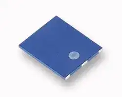
- Centre Frequency: 870MHz
- Antenna Case Size: 16.5mm x 14mm x 0.9mm
| Delivery and price | |
|---|---|
| Units per pack | 500 |
| Price | 3.18 € |
| Current stock | 10+ |
| Lead time | 30 days |
## **WIDE BAND MULTILAYER CERAMIC ANTENNA FOR 850~950MHz**

## **Product Specification[1] (Preliminary)**

## **QUICK REFERENCE DATA**

Working Frequency                            850~950MHz Gain                                                    1.5 dBi Max VSWR                                                2 max Polarization                                         Linear Azimuth Omni-directional Impedance                                           50Ω Operating Temperature -55~125[ o] C Termination Ni/Sn (Environmentally-Friendly Leadless) Resistance to soldering heat 260[o] C, 10 sec.

_Special Environmental Concerns- Green Products Design: The foil making process is using environmentally friendly aqueous solvent technology. Termination is lead free and packing materials can be re-cycled_

|R&D|Print date 02/04/26<br>Preliminary use only|Print date 02/04/26<br>Preliminary use only|Print date 02/04/26<br>Preliminary use only|Print date 02/04/26<br>Preliminary use only|Print date 02/04/26<br>Preliminary use only|Print date 02/04/26<br>Preliminary use only|Print date 02/04/26<br>Preliminary use only|Print date 02/04/26<br>Preliminary use only|
|---|---|---|---|---|---|---|---|---|
||**Multilayer Ceramic Antenna**<br>**(LP Mode) for 850~950MHz**<br>~~es~~|||**4311 119 00087**|||Oct. 24, 01||
||||||||Nov. 6, 01<br>Jan. 7, 02||
||||||||||
|Grant/Cliff.|~~Rs~~|2002-01-07<br>~~Rs~~<br>~~es~~|~~Rs~~|Page1/7<br>~~Rs~~|sheet 190-1<br>~~Rs~~|~~Rs~~|~~Rs~~|A4|
|spec.doc|PHYCOMP Ltd.<br>~~es~~||||||||


## **APPLICATION**

**==> picture [444 x 168] intentionally omitted <==**

**----- Start of picture text -----**<br>
17mm 2mm<br>Suggested Layout (60*20 mm ground plane)<br> Ground plane (back side) Clearance<br>(no ground plane)<br>3mm<br> RF Ceramic<br>Module Antenna<br>3mm<br>**----- End of picture text -----**<br>


50 `•` Transmission Line

## **Solder Land Pattern for Antenna**

|||**_Figure_**||**Dimensions**|**_Remark_**|
|---|---|---|---|---|---|
|S1<br>F<br>S1||L<br>C<br>C<br>S1<br>S2<br>S1<br>W|L<br>W<br>F<br>C<br>S1<br>S2|17.00±0.10 mm<br>14.40±0.10 mm<br>1.00±0.10 mm<br>0.90±0.10 mm<br>1.40±0.10 mm<br>1.00±0.10 mm|Feed pad<br>Mount pad<br>Mount pad|


|R&D|Print date 02/04/26<br>Preliminary use only|Print date 02/04/26<br>Preliminary use only|Print date 02/04/26<br>Preliminary use only|Print date 02/04/26<br>Preliminary use only|Print date 02/04/26<br>Preliminary use only|Print date 02/04/26<br>Preliminary use only|Print date 02/04/26<br>Preliminary use only|Print date 02/04/26<br>Preliminary use only|
|---|---|---|---|---|---|---|---|---|
||**Multilayer Ceramic Antenna**<br>**(LP Mode) for 850~950MHz**|||**4311 119 00087**|||Oct. 24, 01||
||||||||Nov. 6, 01<br>Jan. 7, 02||
||||||||||
|Grant/Cliff.||2002-01-07||Page2/7|sheet 190-2|||A4|
|spec.doc|PHYCOMP Ltd.||||||||


## **MECHANICAL DATA**

|||**Figure**|**Dimension**|**Port**|
|---|---|---|---|---|
|**s1**<br>**s2**<br><br>**s1**<br>**F**<br>**C**<br>**C**|**s1**<br>**s2**<br>|**w**<br>**L**<br>**s1**<br>**F**<br>**s1**<br>**T**<br>**s1**<br>**s2**<br>**s1**<br>**s1**<br>**s1**|L<br>W<br>T<br>F<br>C<br>S1<br>S2<br>16.5`±`0.5mm<br>14.0`±`0.5mm<br>0.9`±`0.2mm<br>0.9`±`0.25mm<br>0.5`±`0.3mm<br>1.25`±`0.35mm<br>0.9`±`0.25mm|-<br>-<br>-<br>Feed termination<br>-<br>Solder termination<br>Solder termination|
||||||


## **Radiation Pattern Polar plot**

**==> picture [203 x 216] intentionally omitted <==**

**----- Start of picture text -----**<br>
-180<br>-135 -225<br>-90 -270<br>-45 45<br>0<br>E Plane<br>**----- End of picture text -----**<br>


**==> picture [191 x 207] intentionally omitted <==**

**----- Start of picture text -----**<br>
-180<br>-135 -225<br>-90 -270<br>-45 45<br>0<br>H Plane<br>**----- End of picture text -----**<br>


|R&D|Print date 02/04/26<br>Preliminary use only|Print date 02/04/26<br>Preliminary use only|Print date 02/04/26<br>Preliminary use only|Print date 02/04/26<br>Preliminary use only|Print date 02/04/26<br>Preliminary use only|Print date 02/04/26<br>Preliminary use only|
|---|---|---|---|---|---|---|
||**Multilayer Ceramic Antenna**<br>**(LP Mode) for 850~950MHz**|||<br>**4311 119 00087**<br> <br>||Oct. 24, 01|
|||||||Nov. 6, 01<br>Jan. 7, 02|
||||||||
|Grant/Cliff.||2002-01-07||Page3/7|sheet 190-3|A4|
|spec.doc|PHYCOMP Ltd.||||||


## **Return Loss Signal**

## **DEMO Board**

**==> picture [180 x 103] intentionally omitted <==**

**----- Start of picture text -----**<br>
90 mm<br>25 mm<br>50 ohm transmission line<br>**----- End of picture text -----**<br>


|R&D|Print date 02/04/26<br>Preliminary use only|Print date 02/04/26<br>Preliminary use only|Print date 02/04/26<br>Preliminary use only|Print date 02/04/26<br>Preliminary use only|Print date 02/04/26<br>Preliminary use only|Print date 02/04/26<br>Preliminary use only|Print date 02/04/26<br>Preliminary use only|Print date 02/04/26<br>Preliminary use only|
|---|---|---|---|---|---|---|---|---|
||**Multilayer Ceramic Antenna**<br>**(LP Mode) for 850~950MHz**|||**4311 119 00087**|||Oct. 24, 01||
||||||||Nov. 6, 01<br>Jan. 7, 02||
||||||||||
|Grant/Cliff.||2002-01-07||Page4/7|sheet 190-4|||A4|
|spec.doc|PHYCOMP Ltd.||||||||


## **RELIABILITY DATA (Reference to IEC Specification)**

|**IEC**<br>**384-10/**<br>**CECC 32**<br>**100**<br>**CLAUSE**|**IEC**<br>**6006868-2**<br>**TEST**<br>**METHOD**|**IEC**<br>**6006868-2**<br>**TEST**<br>**METHOD**|**TEST**|**TEST**|**PROCEDURE**|**PROCEDURE**|**PROCEDURE**|**PROCEDURE**|**REQUIREMENTS**|**REQUIREMENTS**|**REQUIREMENTS**|
|---|---|---|---|---|---|---|---|---|---|---|---|
|4.4|||Mounting||The antenna can be<br>mounted on printed-<br>circuit boards or ceramic<br>substrates by applying<br>wave soldering, reflow<br>soldering (including<br>vapour phase soldering)<br>orconductive adhesive||||No visible damage|||
|4.5|||Visual inspection<br>and dimension<br>check||Any applicable method<br>using× 10 magnification||||In accordance with<br>specification (no chip<br>off3mm)|||
|4.6.1|||Antenna||Central Frequency<br>at20 oC||||Standard test board<br>on page 4|||
|4.8|||Adhesion||A force of 5 N applied for<br>10 s to the line joining the<br>terminations and in a<br>plane parallel to the<br>substrate||||No visible damage|||
|4.9|||Bond strength of<br>plating on end face||Mounted in accordance<br>with CECC 32 100,<br>paragraph 4.4||||No visible damage|||
||||||Conditions: bending 0.25<br>mm at a rate of 1mm/s,<br>radius jig. 340 mm,1 mm<br>warp on FR4 board of 90<br>mm length||||No visible damage|||
|4.10||Tb|Resistance to<br>soldering heat||260±5°C for 10 ± 0.5 s<br>in a static solder bath||||The terminations<br>shall be well tinned<br>after recovery and<br>Central Freq. Change<br>±6%|||
|R&D||Print date 02/04/26||||||||||
|||**Multilayer Ceramic Antenna**<br>**(LP Mode) for 850~950MHz**|||||**4311 119 00087**|||||
|||||||||||||
|||||||||||||
|Grant/Cliff.||||2002-01-07|||Page5/7|sheet 190-5||||
|spec.doc||PHYCOMP Ltd.||||||||||


|**IEC**<br>**384-10/**<br>**CECC 32**<br>**100**<br>**CLAUSE**|**IEC**<br>**6006868-2**<br>**TEST**<br>**METHOD**|**TEST**|**PROCEDURE**|**REQUIREMENTS**|
|---|---|---|---|---|
|||Resistance to<br>leaching|260±5°C for 30 ±1 s in<br>a static solder bath|Using visual<br>enlargement of× 10,<br>dissolution of the<br>termination shall not<br>exceed10%|
|4.11|Ta|Solderability|Zero hour test, and test<br>after storage (20 to 24<br>months) in original<br>atmosphere; un-mounted<br>chips completely<br>immersed for 2±0.5 s in<br>235 ± 5°C.|The termination must<br>be well tinned, at<br>least 75% is well<br>tinned at termination|
|4.12|Na|Rapid change of<br>temperature|-55 °C (30 minutes) to<br>+125°C (30 minutes)**;**<br>100 cycles|No visible damage<br>Central Freq. Change<br>±6%|
|4.14|Ca|Damp heat|500±12 hours at 60°C;<br>90 to 95 % RH|No visible damage<br>2 hours recovery<br>Central Freq. Change<br>±6%|
|4.15||Endurance|500±12 hours at 125°C;|No visible damage<br>2 hours recovery<br>Central Freq. Change<br>±6%|


|R&D|Print date 02/04/26<br>Preliminary use only|Print date 02/04/26<br>Preliminary use only|Print date 02/04/26<br>Preliminary use only|Print date 02/04/26<br>Preliminary use only|Print date 02/04/26<br>Preliminary use only|Print date 02/04/26<br>Preliminary use only|Print date 02/04/26<br>Preliminary use only|Print date 02/04/26<br>Preliminary use only|
|---|---|---|---|---|---|---|---|---|
||**Multilayer Ceramic Antenna**<br>**(LP Mode) for 850~950MHz**|||**4311 119 00087**|||Oct. 24, 01||
||||||||Nov. 6, 01<br>Jan. 7, 02||
||||||||||
|Grant/Cliff.||2002-01-07||Page6/7|sheet 190-6|||A4|
|spec.doc|PHYCOMP Ltd.||||||||


## **ORDERING INFORMATION: 12NC Ordering Code**

The antennas may be ordered by using the 12 NC ordering code.  These code numbers can be determined by the following rules:

4311   1 19 00 087 F  C    M S     T   A

F. Family Code C. Packing Type Code **43** = Antenna **13** = Bulk, 1000 pcs **11 =** 1000 pcs in tape

M. Materials Code

**1** = High Frequency Material

S. Size Code **19** = 16.5 * 14 * 0.9 mm

- T. Tolerance

**00** = 80 M Hz Band Width

- A. Working Frequency

**087 =** 850~950MHz

**Example: 12NC                 4311 119 00087** Product description: Antenna (43) by 1000 pcs (11) of High Frequency Material (1), Size 16.5*14*0.9 mm (19); Tolerance (00) of 80 MHz (VSWR<2) Working Frequency (087) = 850~950MHz

**ORDERING INFORMATION: Method II- by Clear Text Code (Temporary)** The antennas may be ordered by using the 16-digit clear text ordering code.  These code numbers can be determined by the following rules:

|**ORDERING INFORMATION: Method II- by Clear Text Code (Temporary)**<br>The antennas may be ordered by using the 16-digit clear text ordering code.  These code<br>numbers can be determined by the following rules:|**ORDERING INFORMATION: Method II- by Clear Text Code (Temporary)**<br>The antennas may be ordered by using the 16-digit clear text ordering code.  These code<br>numbers can be determined by the following rules:|**ORDERING INFORMATION: Method II- by Clear Text Code (Temporary)**<br>The antennas may be ordered by using the 16-digit clear text ordering code.  These code<br>numbers can be determined by the following rules:|**ORDERING INFORMATION: Method II- by Clear Text Code (Temporary)**<br>The antennas may be ordered by using the 16-digit clear text ordering code.  These code<br>numbers can be determined by the following rules:|**ORDERING INFORMATION: Method II- by Clear Text Code (Temporary)**<br>The antennas may be ordered by using the 16-digit clear text ordering code.  These code<br>numbers can be determined by the following rules:|**ORDERING INFORMATION: Method II- by Clear Text Code (Temporary)**<br>The antennas may be ordered by using the 16-digit clear text ordering code.  These code<br>numbers can be determined by the following rules:|**ORDERING INFORMATION: Method II- by Clear Text Code (Temporary)**<br>The antennas may be ordered by using the 16-digit clear text ordering code.  These code<br>numbers can be determined by the following rules:|
|---|---|---|---|---|---|---|
||||||||
||**AN0870000716141F (Clear Text Code Example)**||||||
|AN|0870|00|07|1614|1|F|
|Product|Central Freq.|Bandwidth|Material|Size|Quantities|Packing|
|AN=<br>Antenna|0870=870MHz<br>~ 950MHz|00= 80MHz|07=K7|1614=16*14*<br>0.9 mm|1 = 1K|F = 13" plastic|


|R&D|Print date 02/04/26<br>Preliminary use only|Print date 02/04/26<br>Preliminary use only|Print date 02/04/26<br>Preliminary use only|Print date 02/04/26<br>Preliminary use only|Print date 02/04/26<br>Preliminary use only|Print date 02/04/26<br>Preliminary use only|Print date 02/04/26<br>Preliminary use only|Print date 02/04/26<br>Preliminary use only|
|---|---|---|---|---|---|---|---|---|
||**Multilayer Ceramic Antenna**<br>**(LP Mode) for 850~950MHz**|||**4311 119 00087**|||Oct. 24, 01||
||||||||Nov. 6, 01<br>Jan. 7, 02||
||||||||||
|Grant/Cliff.||2002-01-07||Page7/7|sheet 190-7|||A4|
|spec.doc|PHYCOMP Ltd.||||||||
Updated at April 22, 2026
Founded in 1977, Yageo Corporation is a premier global provider of passive component solutions. Through strategic acquisitions of industry leaders such as Pulse Electronics, BrightKing, and KEMET, the company has built a comprehensive product portfolio and established a commanding presence across the electronics industry, particularly in capacitors, resistors, and circuit protection technologies. Our extensive range of Yageo components is heavily focused on their advanced circuit protection solutions. We carry a comprehensive selection of transient voltage suppression (TVS) devices, featuring hundreds of TVS diodes and varistors engineered to safeguard sensitive electronics from destructive voltage transients. This core offering is complemented by a robust lineup of gas discharge tubes (GDTs) designed for reliable overvoltage protection in demanding environments. Beyond voltage suppression, we supply a variety of Yageo's specialized thermistor products, including resettable fuses, inrush current limiting (ICL) NTC thermistors, and precision temperature sensing components. Rounding out our selection are high-performance Yageo RF and single-band chip antennas, providing reliable, space-efficient connectivity for modern wireless applications.
About Novapart
Novapart is a B2B electronic component broker specialising in stock shortages and cost reduction. We source hard-to-find parts and identify compliant alternatives across a catalogue of 410,000+ components from 500+ manufacturers.
Learn more →Stock Shortage Specialist
When a component is unavailable, discontinued or has an unacceptable lead time, we tap into our network of vetted European and Asian distributors to source what you need — without compromising on quality or traceability.
Request a quote →Compliant Alternatives
We identify pin-to-pin, electrically equivalent substitutes that meet the same certifications (RoHS, AEC-Q100, REACH) as your original specification — validated against datasheets, not just part numbers. Often at a lower cost.
BOM Analysis service →