


CAN4311714002454K
ANTENNA, 2012, WLAN, 2.45GHZ
- Manufacturer: YAGEO
- Product type: Antennas - Single Band Chip
- Centre Frequency: 2.45GHz
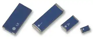
- Antenna Case Size: 2mm x 1.2mm x 1.1mm
| Delivery and price | |
|---|---|
| Units per pack | 6000 |
| Price | 0.39 € |
| Current stock | 10+ |
| Lead time | 30 days |
## _**ANTENNA PRODUCTS**_

## DATA SHEET **2012 Ceramic Chip Antenna for Bluetooth/WLAN Application**

Feb, 2007 V1 Print date 07/06/05 Feb, 2007 **2012 Ceramic Chip Antenna for Bluetooth/WLAN Application CAN4311714XX2454K** Justin Liu ~~ee:~~ C.T.Lee Page 1 sheet 190-1 A4 spec.doc Yageo Taiwan

## **2012 Ceramic Chip Antenna for Bluetooth/WLAN Application**

## **Quick Reference Data**

Centre Frequency 2.45 GHz* ¹ Bandwidth                                        at least 70 MHz* ² VSWR                                               2.5 (Max.)* ² Polarization                                       Linear Azimuth Beamwidth                       Omni-directional Peak Gain                                           4.0 dBi* ² Impedance                                         50 Ω Operating Temperature -55~125[ o] C Termination                                      Ni / Sn (Environmentally-Friendly Leadless) Resistance to soldering heats            260 ℃ , 10sec. Maximum Power                              1W

1 All the technical data and information contained herein are subject to change without prior notice **2** Testing under evaluation board of page 4

||Print date 07/06/05<br>|Print date 07/06/05<br>|Print date 07/06/05<br>|Print date 07/06/05<br>|Print date 07/06/05<br>|Print date 07/06/05<br>|Print date 07/06/05<br>|Print date 07/06/05<br>|
|---|---|---|---|---|---|---|---|---|
||**2012 Ceramic Chip Antenna**<br>**for Bluetooth/WLAN Application**|||**CAN4311714XX2454K**|||Feb, 2007||
||||||||||
||||||||||
|Justin Liu|C.T.Lee|||Page2|sheet 190-2|||A4|
|spec.doc|Yageo Taiwan||||||||


## **1. Mechanical Data (2.0 x 1.25 x 1.1 mm)**

**==> picture [152 x 90] intentionally omitted <==**

**----- Start of picture text -----**<br>
2.0+/-0.2mm<br>+<br>1.25+/-0.2mm<br>**----- End of picture text -----**<br>


**Unit: mm**

## **2. Layout of Soldering Pads**

**==> picture [151 x 153] intentionally omitted <==**

**----- Start of picture text -----**<br>
1.0 +/-0.1mm<br>1.7 +/-0.1mm<br>0.4 +/-0.1mm<br><<»<br>1.4 +/-0.1mm<br>**----- End of picture text -----**<br>


||Print date 07/06/05<br>|Print date 07/06/05<br>|Print date 07/06/05<br>|Print date 07/06/05<br>|Print date 07/06/05<br>|Print date 07/06/05<br>|Print date 07/06/05<br>|Print date 07/06/05<br>|
|---|---|---|---|---|---|---|---|---|
||**2012 Ceramic Chip Antenna**<br>**for Bluetooth/WLAN Application**<br>~~ee~~<br>~~ee~~|||**CAN4311714XX2454K**|||Feb, 2007||
||||||||||
||||||||||
|Justin Liu|C.T.Lee<br>~~es~~|~~es~~<br>~~ee~~|~~es~~<br>~~ee~~|Page3<br>~~es~~|sheet 190-3<br>~~es~~|~~es~~|~~es~~|A4|
|spec.doc|Yageo Taiwan<br>~~ee~~<br>~~ee~~||||||||


## **3. Dimension and Outlook of Evaluation Board**

**==> picture [145 x 260] intentionally omitted <==**

**----- Start of picture text -----**<br>
18<br><><br>0.5 a 10<br>__ aes<br>2<br>30<br>50 ohm Line<br>Unit:mm<br>**----- End of picture text -----**<br>


**Unit: mm**

||Print date 07/06/05<br>|Print date 07/06/05<br>|Print date 07/06/05<br>|Print date 07/06/05<br>|Print date 07/06/05<br>|Print date 07/06/05<br>|Print date 07/06/05<br>|Print date 07/06/05<br>|
|---|---|---|---|---|---|---|---|---|
||**2012 Ceramic Chip Antenna**<br>**for Bluetooth/WLAN Application**<br>~~ee~~<br>~~ee~~|||**CAN4311714XX2454K**|||Feb, 2007||
||||||||||
||||||||||
|Justin Liu|C.T.Lee<br>~~es~~|~~es~~<br>~~ee~~|~~es~~<br>~~ee~~|Page4<br>~~es~~|sheet 190-4<br>~~es~~|~~es~~|~~es~~|A4|
|spec.doc|Yageo Taiwan<br>~~ee~~<br>~~ee~~||||||||


## **4. Measurement of S-parameter**

||Print date 07/06/05<br>|Print date 07/06/05<br>|Print date 07/06/05<br>|Print date 07/06/05<br>|Print date 07/06/05<br>|Print date 07/06/05<br>|Print date 07/06/05<br>|Print date 07/06/05<br>|
|---|---|---|---|---|---|---|---|---|
||**2012 Ceramic Chip Antenna**<br>**for Bluetooth/WLAN Application**|||**CAN4311714XX2454K**|||Feb, 2007||
||||||||||
||||||||||
|Justin Liu|C.T.Lee|||Page5|sheet 190-5|||A4|
|spec.doc|Yageo Taiwan||||||||


**5.The Environment of Antenna Radiation Pattern Anechoic Chamber Dimension=8(m)** **`×` 4(m)** **`×` 4(m)**

||Print date 07/06/05<br>|Print date 07/06/05<br>|Print date 07/06/05<br>|Print date 07/06/05<br>|Print date 07/06/05<br>|Print date 07/06/05<br>|Print date 07/06/05<br>|Print date 07/06/05<br>|
|---|---|---|---|---|---|---|---|---|
||**2012 Ceramic Chip Antenna**<br>**for Bluetooth/WLAN Application**|||**CAN4311714XX2454K**|||Feb, 2007||
||||||||||
||||||||||
|Justin Liu|C.T.Lee|||Page6|sheet 190-6|||A4|
|spec.doc|Yageo Taiwan||||||||


## **6. 3D Radiation Pattern ( 40x18 mm demo board)**

## **7. Layout Recommendation in Application**

||Print date 07/06/05<br>|Print date 07/06/05<br>|Print date 07/06/05<br>|Print date 07/06/05<br>|Print date 07/06/05<br>|Print date 07/06/05<br>|Print date 07/06/05<br>|Print date 07/06/05<br>|
|---|---|---|---|---|---|---|---|---|
||**2012 Ceramic Chip Antenna**<br>**for Bluetooth/WLAN Application**|||**CAN4311714XX2454K**|||Feb, 2007||
||||||||||
||||||||||
|Justin Liu|C.T.Lee|||Page7|sheet 190-7|||A4|
|spec.doc|Yageo Taiwan||||||||


**==> picture [442 x 650] intentionally omitted <==**

**----- Start of picture text -----**<br>
Ant<br>Empty area<br>Feed<br>Ground<br>100mm<br>| |<br>]~—_+|<br>40mm<br>12.5*5 mm clearance<br>Ground<br>50 ohm Line<br>Dimension of Demo Board<br>100*40 mm<br>Unit:mm<br>a<br>Print date 07/06/05<br>Feb, 2007<br>2012 Ceramic Chip Antenna<br>for Bluetooth/WLAN Application  CAN4311714XX2454K<br>Justin Liu ss C.T.Lee  Page 8 sheet 190-8   A4<br>spec.doc Yageo Taiwan<br>**----- End of picture text -----**<br>


|**IEC**<br>**384-10/**<br>**CECC 32**<br>**100**<br>**CLAUSE**|**IEC**<br>**60068-2**<br>**TEST**<br>**METHOD**|**TEST**|**PROCEDURE**|**REQUIREMENTS**|
|---|---|---|---|---|
|4.4||Mounting|The antenna can be<br>mounted on printed-circuit<br>boards or ceramic<br>substrates by applying<br>wave soldering, reflow<br>soldering (including<br>vapour phase soldering) or<br>conductive adhesive|No visible damage|
|4.5||Visual inspection<br>and dimension<br>check|Any applicable method<br>using**× **10 magnification|In accordance with<br>specification (chip off<br>4mm)|
|4.6.1||Antenna|Central Frequency<br>at20 oC|Standard test board in<br>page 4|
|4.8||Adhesion|A force of 3 N applied for<br>10 s to the line joining the<br>terminations and in a<br>plane parallel to the<br>substrate|No visible damage|
|4.9||Bond strength of<br>plating on end face|Mounted in accordance<br>with CECC 32 100,<br>paragraph 4.4|No visible damage|
||||Conditions: bending 0.5<br>mm at a rate of 1mm/s,<br>radius jig. 340 mm, 2mm<br>warp on FR4 board of 90<br>mm length|No visible damage|
|4.10|20(Tb)|Resistance to<br>soldering heat|260±5°C for 10 ± 0.5 s<br>in a static solder bath|The terminations shall<br>be well tinned after<br>recovery and<br>Central Freq. Change<br>± 6%|
|||Resistance to<br>leaching|260±5°C for 30 ±1 s in<br>a static solder bath|Using visual<br>enlargement of**× **10,<br>dissolution of the<br>termination shall not<br>exceed10%|


||Print date 07/06/05<br>|Print date 07/06/05<br>|Print date 07/06/05<br>|Print date 07/06/05<br>|Print date 07/06/05<br>|Print date 07/06/05<br>|Print date 07/06/05<br>|Print date 07/06/05<br>|
|---|---|---|---|---|---|---|---|---|
||**2012 Ceramic Chip Antenna**<br>**for Bluetooth/WLAN Application**|||**CAN4311714XX2454K**|||Feb, 2007||
||||||||||
||||||||||
|Justin Liu|C.T.Lee|||Page9|sheet 190-9|||A4|
|spec.doc|Yageo Taiwan||||||||


|**IEC**<br>**384-10/**<br>**CECC 32**<br>**100**<br>**CLAUSE**|**IEC**<br>**60068-2**<br>**TEST**<br>**METHOD**|**TEST**|**PROCEDURE**|**REQUIREMENTS**|
|---|---|---|---|---|
|4.11|20(Ta)|Solderability|Zero hour test, and test<br>after storage (20 to 24<br>months) in original<br>atmosphere; un-mounted<br>chips completely<br>immersed for 2±0.5 s in<br>235 ±5°C.|The termination must<br>be well tinned, at least<br>75% is well tinned at<br>termination|
|4.12|4(Na)|Rapid change of<br>temperature|-25 °C (30 minutes) to +85<br>°C (30 minutes)**;**100<br>cycles|No visible damage<br>Central Freq. Change<br>±6%|
|4.14|3(Ca)|Damp heat|500±12 hours at 60°C;<br>90 to 95 % RH|No visible damage<br>2 hours recovery<br>Central Freq. Change<br>± 6%|
|4.15||Endurance|500±12 hours at 85°C;|No visible damage<br>2 hours recovery<br>Central Freq. Change<br>± 6%|


||Print date 07/06/05<br>|Print date 07/06/05<br>|Print date 07/06/05<br>|Print date 07/06/05<br>|Print date 07/06/05<br>|Print date 07/06/05<br>|Print date 07/06/05<br>|Print date 07/06/05<br>|
|---|---|---|---|---|---|---|---|---|
||**2012 Ceramic Chip Antenna**<br>**for Bluetooth/WLAN Application**|||**CAN4311714XX2454K**|||Feb, 2007||
||||||||||
||||||||||
|Justin Liu|C.T.Lee|||Page10|sheet 190-<br>10|||A4|
|spec.doc|Yageo Taiwan||||||||


## **Ordering Information**

The antennas may be ordered by using the Yageo ordering code.  These code numbers can be determined by the following rules:

## **CAN43 11 7 14 XX 245 4K**

Family Code **CAN 43** = Yageo Part No. for Antenna

Packing Type Code

**11** = 180 mm/ 7" reel , blister taping

Materials Code **7** = High Frequency Material

Size Code

**11** = 3.2 * 2.5 **12** = 3.2 * 1.6 **13** = 2.5 * 2.0 **14** = 2.0 * 1.2 **15** = 1.6 * 0.8

Antenna type **00** = normal type 02 = Type 2 03 = Type 3 04 = Type 4 05 = Type 5 06 = Type 6 07 = Type 7 08 = Type 8 09 = Type 9

Working Frequency **245 =** 2.45 GHz

## Packing Type Code

||Print date 07/06/05<br>|Print date 07/06/05<br>|Print date 07/06/05<br>|Print date 07/06/05<br>|Print date 07/06/05<br>|Print date 07/06/05<br>|Print date 07/06/05<br>|Print date 07/06/05<br>|
|---|---|---|---|---|---|---|---|---|
||**2012 Ceramic Chip Antenna**<br>**for Bluetooth/WLAN Application**|||**CAN4311714XX2454K**|||Feb, 2007||
||||||||||
||||||||||
|Justin Liu|C.T.Lee|||Page11|sheet 190-<br>11|||A4|
|spec.doc|Yageo Taiwan||||||||


## **4K =** 4000 pcs for taping per reel

## **Taping Blister Tape**

## **DIMENSION:**

|Serial no<br>~~a~~|Cecking note<br>|Index<br>|Spec(mm)<br>|
|---|---|---|---|
|1<br>~~eG~~|Sprocket hole<br>~~eG~~|Do<br>~~eG~~|1.50±0.10<br>~~eG~~|
|2<br>~~eG~~|Pocket hole<br>~~eG~~|D1<br>~~eG~~|≥1<br>~~eG~~|
|3<br>~~eG~~|Distance sprocket hole/sprocket hole<br>~~eG~~|Po<br>~~eG~~|4.0±0.10<br>~~eG~~|
|4<br>~~eG~~|Distance pocket/pocket<br>~~eG~~|P1<br>~~eG~~|4.0±0.10<br>~~eG~~|
|5<br>~~eG~~|Distance sprocket hole/pocket<br>~~eG~~|P2<br>~~eG~~|2.0±0.10<br>~~eG~~|
|6<br>~~eG~~|Tape width<br>~~eG~~|W<br>~~eG~~|8.1±0.20<br>~~eG~~|
|7<br>~~eG~~|Distance sprocket hole/outside<br>~~eG~~|E<br>~~eG~~|1.75±0.10<br>~~eG~~|
|8<br>~~eG~~|Distance sprocket hole/pocket<br>~~eG~~|F<br>~~eG~~|3.5±0.0.05<br>~~eG~~|
|9<br>~~eG~~|Pocket length nominal clearance<br>~~eG~~|Ao<br>~~eG~~|1.42±0.10<br>~~eG~~|
|10<br>~~eG~~|Pocket length nominal clearance<br>~~eG~~|Bo<br>~~eG~~|2.24±0.10<br>~~eG~~|
|11<br>~~eG~~|Pocket depth minimum clearance<br>~~eG~~|Ko<br>~~eG~~|1.2±0.10<br>~~eG~~|
|12<br>~~eG~~|Thickness of tape<br>~~eG~~|T<br>~~eG~~<br>~~D~~|0.22±0.05<br>~~eG~~|
|13<br>~~ee~~|10x sprocket hole pitch<br>~~ee~~|10Po<br>~~ee~~<br>~~D~~|40.0±0.20<br>~~ee~~|


||Print date 07/06/05||||||||
|---|---|---|---|---|---|---|---|---|
||||||||Feb, 2007||
||**2012 Ceramic Chip Antenna**||||||||
||**for Bluetooth/WLAN Application**|||**CAN4311714XX2454K**|||||
||||||||||
|Justin Liu|C.T.Lee|||Page13|sheet 190-<br>13|||A4|
|spec.doc|Yageo Taiwan||||||||


## **7 ” (180mm) Reel Specifications**

|**Product size**<br>**code**|**Units per**<br>**Reel **|**Tape Width**<br>**(mm)**|**C**<br> **(mm)**|**D**<br>**(mm)**|**W1 **<br>**(mm)**|**W2**<br>**(mm)**|
|---|---|---|---|---|---|---|
|Antenna|4000|8|180.0±1.0|62±1.5|8.4+/-0.15|14.4 max|


||Print date 07/06/05<br>|Print date 07/06/05<br>|Print date 07/06/05<br>|Print date 07/06/05<br>|Print date 07/06/05<br>|Print date 07/06/05<br>|Print date 07/06/05<br>|Print date 07/06/05<br>|
|---|---|---|---|---|---|---|---|---|
||**2012 Ceramic Chip Antenna**<br>**for Bluetooth/WLAN Application**<br>~~fT~~<br>~~|~~<br>~~[|~~|||**CAN4311714XX2454K**<br>~~[|~~<br>~~|~~<br>~~dL~~|||Feb, 2007||
||||||||||
|~~fT~~|||||||~~dL~~||
|Justin Liu<br>~~fT~~|C.T.Lee<br>~~fT~~<br>~~|~~|~~[|~~|~~[|~~|Page14<br>~~[|~~<br>~~|~~|sheet 190-<br>14<br>~~dL~~|~~dL~~|~~dL~~|A4|
|spec.doc<br>~~fT~~|Yageo Taiwan<br>~~fT~~<br>~~|~~<br>~~[|~~<br>~~|~~<br>~~dL~~||||||||


## **Revision Control:**

|Revision|Date||Content|Remark|
|---|---|---|---|---|
|V1|Feb, 2007|New Issued|||


||Print date 07/06/05<br>|Print date 07/06/05<br>|Print date 07/06/05<br>|Print date 07/06/05<br>|Print date 07/06/05<br>|Print date 07/06/05<br>|Print date 07/06/05<br>|Print date 07/06/05<br>|
|---|---|---|---|---|---|---|---|---|
||**2012 Ceramic Chip Antenna**<br>**for Bluetooth/WLAN Application**|||**CAN4311714XX2454K**|||Feb, 2007||
||||||||||
||||||||||
|Justin Liu|C.T.Lee|||Page15|sheet 190-<br>15|||A4|
|spec.doc|Yageo Taiwan||||||||
Updated at February 9, 2023
Founded in 1977, Yageo Corporation is a premier global provider of passive component solutions. Through strategic acquisitions of industry leaders such as Pulse Electronics, BrightKing, and KEMET, the company has built a comprehensive product portfolio and established a commanding presence across the electronics industry, particularly in capacitors, resistors, and circuit protection technologies. Our extensive range of Yageo components is heavily focused on their advanced circuit protection solutions. We carry a comprehensive selection of transient voltage suppression (TVS) devices, featuring hundreds of TVS diodes and varistors engineered to safeguard sensitive electronics from destructive voltage transients. This core offering is complemented by a robust lineup of gas discharge tubes (GDTs) designed for reliable overvoltage protection in demanding environments. Beyond voltage suppression, we supply a variety of Yageo's specialized thermistor products, including resettable fuses, inrush current limiting (ICL) NTC thermistors, and precision temperature sensing components. Rounding out our selection are high-performance Yageo RF and single-band chip antennas, providing reliable, space-efficient connectivity for modern wireless applications.
About Novapart
Novapart is a B2B electronic component broker specialising in stock shortages and cost reduction. We source hard-to-find parts and identify compliant alternatives across a catalogue of 410,000+ components from 500+ manufacturers.
Learn more →Stock Shortage Specialist
When a component is unavailable, discontinued or has an unacceptable lead time, we tap into our network of vetted European and Asian distributors to source what you need — without compromising on quality or traceability.
Request a quote →Compliant Alternatives
We identify pin-to-pin, electrically equivalent substitutes that meet the same certifications (RoHS, AEC-Q100, REACH) as your original specification — validated against datasheets, not just part numbers. Often at a lower cost.
BOM Analysis service →