
Image not available
Illustrative purposes only

C6D06065A
Silicon Carbide Schottky Diode, Z-Rec, Single, 650 V, 24 A, 23 nC, TO-220
⚠️ Reference pricing provided. In case of supply shortages, we will connect you with our trusted procurement partners to ensure your project's continuity.
- Manufacturer: WOLFSPEED
- Product type: Silicon Carbide Schottky Diodes
- Product Range:Z-Rec Series; Diode Configuration:Single; Repetitive Reverse Voltage Vrrm Max:650V; Continuous Forward Current If:24A; Total Capacitive Charge Qc:23nC; Diode Case S
- SVHC: To Be Advised
- No. of Pins: 2 Pin
- Product Range: Z-Rec
- Qualification: -
- Diode Mounting: Through Hole
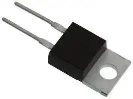
- Diode Case Style: TO-220
- Diode Configuration: Single
- Average Forward Current: 24A
- Total Capacitive Charge: 23nC
- Operating Temperature Max: 175°C
- Repetitive Peak Reverse Voltage: 650V
| Delivery and price | |
|---|---|
| Units per pack | 1000 |
| Price | 0.996 € |
| Current stock | 500+ |
| Lead time | 30 days |
Datasheet

## **C6D06065A**

## **Silicon Carbide Schottky Diode**

## _Z-Rec[®]_ Rectifier

## **Features**

## **Package**

**==> picture [101 x 51] intentionally omitted <==**

**----- Start of picture text -----**<br>
V =       650 V<br>RRM<br>IF (TC=155˚C) =          6 A<br>Qc                 =      23 nC<br>**----- End of picture text -----**<br>


- New 6[th] Generation Technology

- Low Forward Voltage Drop (VF)

- Zero Reverse Recovery Current

- Zero Forward Recovery Voltage

- Low Leakage Current (Ir)

- Temperature-Independent Switching Behavior

- Positive Temperature Coefficient on VF

**==> picture [60 x 7] intentionally omitted <==**

**----- Start of picture text -----**<br>
          TO-220-2<br>**----- End of picture text -----**<br>


## **Benefits**

- Higher System Level Efficiency

- Increase System Power Density

**==> picture [146 x 27] intentionally omitted <==**

**----- Start of picture text -----**<br>
PIN 1<br>CASE<br>PIN 2<br>**----- End of picture text -----**<br>


- Reduction of Heat Sink Requirements

- Parallel Devices Without Thermal Runaway

## **Applicationspplicationslications**

**Applicationspplicationslications Part Number Package Marking** Switch Mode Power Supplies (SMPS) C6D06065A TO-220-2 C6D06065 Server/Telecom Power Supplies ~~Ea~~ Industrial Power Supplies Solar UPS **Maximum Ratings** (TC = 25 ˚C unless otherwise specified)C = 25 ˚C unless otherwise specified) = 25 ˚C unless otherwise specified) **Symbol Parameter Value Unit Test Conditions Note** ~~ee~~ VRRM Repetitive Peak Reverse Voltage 650 V ~~a ee ee ee~~ VDC DC Blocking Voltage 650 V ~~a~~ ~~**ee ee** eeee~~ ~~**ee ee**~~ 24 TC=25˚C IF Continuous Forward Current 12 A TC=125˚C Fig. 3 ~~Pf~~ 6 TC=155˚C ~~e~~ IFRM Repetitive Peak Forward Surge Current ~~e~~ 2817 ~~**e** ee~~ A TTCC=25˚C, t=110˚C, tP = 10 ms, Half Sine Wave P=10 ms, Half Sine Wave ~~eee e~~ IFSM Non-Repetitive Peak Forward Surge Current ~~e~~ 5146 ~~**e** ee~~ A TTCC=25˚C, t=110˚C, tp = 10 ms, Half Sine Wave p = 10 ms, Half Sine Wave ~~eee~~ Fig. 8 ~~e~~ IF,Max Non-Repetitive Peak Forward Surge Current ~~e~~ 520470 ~~**e** ee~~ A TTCC=25˚C, t=110˚C, tP = 10 µs, PulseP = 10 µs, Pulse ~~eee~~ Fig. 8 ~~e~~ Ptot Power Dissipation ~~e~~ 7332 ~~**e** ee~~ W TTCC=25˚C=110˚C ~~eee~~ Fig. 4 -55 to TJ , Tstg Operating Junction and Storage Temperature +175 ˚C ~~ee~~ ~~**e** ee eee~~ 1 Nm M3 Screw TO-220 Mounting Torque 8.8 lbf-in 6-32 Screw ~~ee~~ ~~**e** ee ee~~

- Switch Mode Power Supplies (SMPS)

- Server/Telecom Power Supplies

- Industrial Power Supplies

- Solar

- UPS

**Maximum Ratings** (TC = 25 ˚C unless otherwise specified)C = 25 ˚C unless otherwise specified) = 25 ˚C unless otherwise specified)

**1** C6D06065A, Rev. -, 04-2019

## **Electrical Characteristics**

**==> picture [543 x 29] intentionally omitted <==**

**----- Start of picture text -----**<br>
Symbol Parameter Typ. Max. Unit Test Conditions Note<br>**----- End of picture text -----**<br>


|**Symbol**|**Parameter**|**Typ.**|**Max.**|**Unit**|**Test Conditions**|**Note**|
|---|---|---|---|---|---|---|
||||||||
|VF|Forward Voltage|1.27<br>1.37|1.50<br>1.60|V|IF= 6 A  TJ=25°C<br>IF= 6 A  TJ=175°C|Fig. 1|
|IR|Reverse Current|2<br>15|30<br>120|μA|VR= 650 V  TJ=25°C<br>VR= 650 V  TJ=175°C|Fig. 2|
|QC|Total Capacitive Charge|23||nC|VR= 400 V, IF= 6 A<br>TJ= 25°C|Fig. 5|
|C|Total Capacitance|394<br>44<br>36||pF|VR= 0 V, TJ= 25°C, f = 1 MHz<br>VR= 200 V, TJ= 25˚C, f = 1 MHz<br>VR= 400 V, TJ= 25˚C, f = 1 MHz|Fig. 6|
|EC|Capacitance Stored Energy|3.5||μJ|VR= 400 V|Fig. 7|


Note: This is a majority carrier diode, so there is no reverse recovery charge.

## **Thermal Characteristics**

|**Symbol**|**Parameter**|**Typ.**|**Unit**|**Note**|
|---|---|---|---|---|
|RθJC|Thermal Resistance from Junction to Case|2.05|°C/W|Fig. 9|


**==> picture [643 x 344] intentionally omitted <==**

**----- Start of picture text -----**<br>
Typical Performance<br>20 100<br>18<br>TJ = -55°C<br>16 TJ = 25°C 80<br>TJ = 75°C<br>14 TJ = 125°C<br>TJ = 175°C<br>12 60<br>TJ = 175 °C<br>10<br>TJ = 125 °C<br>8 40<br>TJ = 75 °C<br>6<br>TJ = 25 °C<br>4<br>20<br>TJ = -55 °C<br>2<br>0<br>0<br>0.5 1.0 1.5 2.0 2.5<br>0 100 200 300 400 500 600 700 800<br>Foward Voltage, V VVVFVFF (V) (V) (V)F (V) F (V) Reverse Voltage, V VVVRRR (V) (V) (V) R (V)<br> (uA)<br> (A)<br>F RR<br>A)<br> (A) A)A) m<br> (A) (A) (A) (A)IIIIIFFFFF  (I (I m  (I m RRR<br>Foward Current, I Reverse Leakage Current, I<br>**----- End of picture text -----**<br>


Figure 1. Forward Characteristics

Figure 2. Reverse Characteristics

C6D06065A, Rev. -, 04-2019

**2**

**==> picture [640 x 704] intentionally omitted <==**

**----- Start of picture text -----**<br>
Typical Performance<br>80 80 14 70<br>10% Duty10% Duty<br>70 20% Duty20% Duty 70 12 60<br>30% Duty30% Duty<br>50% Duty50% Duty<br>60 60<br>70% Duty70% Duty 10 50<br>DCDC<br>50 50<br>40 8<br>40 40<br>30 6<br>30 30<br>20 4<br>20 20<br>10 1010 2<br>0 0 0 0<br>25 50 75 100 125 15015 175175 25 2525 50 50 75 75 100 100 125 125 150 150 175 175<br>T T TTTC C CCC ˚C  (°C)  ˚C ˚C ˚C TTT T TC C CC C  ˚CC  (°C)  ˚C ˚C ˚C<br>Figure 3. Current Derating Figure 4. Power Derating<br>35 12 180 450<br>Conditions: Conditions: Conditions: Conditions:<br>30 T T J J  = 25 °C  = 25 °C 160 400 T T J J  = 25 °C  = 25 °C<br>10 F F test test  = 1 MHz  = 1 MHz<br>140 350 V V test test  = 25 mV  = 25 mV<br>25<br>8 120 300<br>20<br>100 250<br>6<br>200 80<br>15<br>4 150 60<br>10<br>100 40<br>2<br>5<br>20 50<br>0 0 0 0<br>0 0 100 100 200 200 300 300 400 400 500 500 600 600 700 700 0 0 1 1 10 10 100 100 1000 1000<br>Reverse Voltage, V Reverse Voltage, V VVVVVRRRR (V) (V)R (V) (V) (V) R R  (V)  (V) Reverse Voltage, V Reverse Voltage, V VVVRR (V)RR (V) (V) R R  (V)  (V)<br> (A) (A) (A) (A)  (A)IF  (W) (W)  (W)  (W)  (W) TotTotTotTot<br>IIIIF(peak)F(peak)F(peak)F(peak) PPP PPTOTTOT<br> (W)<br>Tot<br>P<br> (nC)  (nC)<br>C C<br> (nC) (nC)Q (nC) (nC)QQ (nC)QC (pF)CCCCC C (pF)C (pF)C (pF)<br>Q<br>tive Charge, Q apacitance (pF)C Capacitance (pF)<br>Capacitive Charge, Q Capaci<br>**----- End of picture text -----**<br>


Figure 5. Total Capacitance Charge vs. Reverse Voltage

Figure 6. Capacitance vs. Reverse Voltage

C6D06065A, Rev. -, 04-2019

**3**

**==> picture [645 x 753] intentionally omitted <==**

**----- Start of picture text -----**<br>
Typical Performance<br>912 121,000<br>8<br>10 10<br>7 TJ_initial = 25 °C<br>TJ_initial = 110 °C<br>68 8<br>5<br>6 6100<br>4<br>34 4<br>2<br>2 2<br>1<br>10<br>00 0<br>10E-6 100E-6 1E-3 10E-3<br>00 10100 20200 300300 400400 500500 600600 700 0 100 200 300 400 500 600 700<br>Reverse Voltage, VReverse Voltage, V VR (V) RR (V) (V) Reverse Voltage, VTime, t tp (s) p (s) R (V)<br>Figure 7. Capacitance Stored Energy Figure 8. Non-repetitive peak forward surge current<br>versus pulse duration (sinusoidal waveform)<br>0.50.5<br>10  1 1 0.3<br>0.5 0.3<br>0.1<br>0.3 0.1<br>0.05<br>0.05<br>100E-30 1 0.1 0.02<br>0.02<br>0.01<br>0.05<br>0.01<br>SinglePulseSinglePulse<br>0.02<br>100E-3 10E-3E 3 0.01 SinglePulse<br>10E-3 1E-33<br>1E-6 1E-61E-6 10E-6 10E-610E-6 100E-6 100E-6100E-6 1E-3 10E-3 1E-31E-3 100E-3 10E-310E-3 1 100E-3100E-3 10 100  1 1<br>Time, tTime, t T (Sec)T (Sec)T (Sec)T (Sec)T (Sec) pp (s) (s)<br>Figure 9. Transient Thermal Impedance<br>J) J)<br>m m<br> (  (<br>C C<br>J) m J)  (A)  (A)<br>(C ( m IFSM FSM<br>E C I<br>E<br>nce<br>Capacitance Stored Energy, E Capacitance Stored Energy, E<br>C/W) (C/W)o (o<br>thJCthJC<br>Z<br>e<br>Thermal Resistance (˚C/W)Thermal Resistance (˚C/W)Thermal Resistance (˚C/W)Thermal Resistance (˚C/W)Thermal Resistance (˚C/W)<br>Junction To Case Impedance, Z<br>**----- End of picture text -----**<br>


C6D06065A, Rev. -, 04-2019

**4**

**==> picture [124 x 118] intentionally omitted <==**

**----- Start of picture text -----**<br>
» [[4]]<br>Package Dimensionsge Dimensionse Dimensions<br>Package TO-220-2<br>| ;<br>_<br>**----- End of picture text -----**<br>


**==> picture [496 x 441] intentionally omitted <==**

**----- Start of picture text -----**<br>
||||||||||||||||
|---|---|---|---|---|---|---|---|---|---|---|---|---|---|---|
|»|[[4]]|
|Package Dimensionsge Dimensionse Dimensions|
|Package TO-220-2|
|||;|||POS|Min|Inches|Max|MinMillimetersMax|
|A|.381|.410|9.677|10.414|
|_|fr|eeesee|ee|ee|ee|
|TD|B|.235|.255|5.969|6.477|
|||ee|ee|ee|ee|
|C|.100|.120|2.540|3.048|
|:|
|fe|D|.223|.337|5.664|8.560|
|||||ee|ee|||
|D1|.457-.490|11.60-12.45 typ|
|||||es|D2|.277-.303 typ|ee||7.04-7.70 typ|ee|
|D3|.244-.252 typ|6.22-6.4 typ|
|Ion|—-})|._—_|||||||||es|E1E|.590.302|ee|.615.326|ee|14.9867.68|ee|15.6218.28|
|ee|ee|ee|ee|ee|
|E2|.227|251|5.77|6.37|
|rs|ee|ee|ee|ee|
|||F|.143|.153|3.632|3.886|
|||W|||G|1.105|1.147|28.067|29.134|
|7|H|.500|.550|12.700|13.970|
|es|es|ee|ee|ee|
|L|.025|.036|.635|.914|
|es|ee|ee|ee|ee|
|.|M|.045|.055|1.143|1.550|
|ee|ee|ee|ee|
|N|.195|.205|4.953|5.207|
|A|pee|o¥|es|es|ee|ee|ee|
|||hy|4Hh|i;|QP|.048.165|.054.185|1.2194.191|1.3724.699|
|ee|ee|ee|es|
|S|3°|6°|3°|6°|
|Po|ana|an|es|ee|ee|ee|ee|
|T|3°|6°|3°|6°|
|L—|__|i|U|3°|6°|3°|6°|
|V|.094|.110|2.388|2.794|
|PIN 1|W|.014|.025|.356|.635|
|CASE|X|3°|5.5°|3°|5.5°|
|ee|ee|ee|
|PIN 2|Y|.385|.410|9.779|10.414|
|||Lo|
|z|.130|.150|3.302|3.810|
|ee|ee|ee|ee|ee|
|View A-A|NOTE:|
|1.|Dimension L, M, W apply for Solder Dip Finish|

**----- End of picture text -----**<br>


## **Recommended Solder Pad Layout**

## TO-220-2

**==> picture [215 x 30] intentionally omitted <==**

**----- Start of picture text -----**<br>
||||
|---|---|---|
|Part Number|Package|Marking|
|C6D06065A|TO-220-2|C6D06065|

**----- End of picture text -----**<br>


**Note: Recommended soldering profiles can be found in the applications note here:** http://www.wolfspeed.com/power_app_notes/soldering

C6D06065A, Rev. -, 04-2019

**5**

## **Notes**

- **RoHS Compliance**

   - The levels of RoHS restricted materials in this product are below the maximum concentration values (also referred to as the threshold limits) permitted for such substances, or are used in an exempted application, in accordance with EU Directive 2011/65/EC (RoHS2), as implemented January 2, 2013. RoHS Declarations for this product can be obtained from your Wolfpseed representative or from the Product Ecology section of our website at http://www.wolfspeed.com/Power/Tools-and-Support/Product-Ecology.

## **• REACh Compliance**

REACh substances of high concern (SVHCs) information is available for this product. Since the European Chemical Agency (ECHA) has published notice of their intent to frequently revise the SVHC listing for the foreseeable future,please contact a Cree representative to insure you get the most up-to-date REACh SVHC Declaration. REACh banned substance information (REACh Article 67) is also available upon request.

- This product has not been designed or tested for use in, and is not intended for use in, applications implanted into the human body nor in applications in which failure of the product could lead to death, personal injury or property damage, including but not limited to equipment used in the operation of nuclear facilities, life-support machines, cardiac defibrillators or similar emergency medical equipment, aircraft navigation or communication or control systems, or air traffic control systems.

## **Related Links**

- Cree SiC Schottky diode portfolio: http://www.wolfspeed.com/Power/Products#SiCSchottkyDiodes

- Schottky diode Spice models: http://www.wolfspeed.com/power/tools-and-support/DIODE-model-request2

- SiC MOSFET and diode reference designs: http://go.pardot.com/l/101562/2015-07-31/349i

Copyright © 2019 Cree, Inc. All rights reserved. The information in this document is subject to change without notice. Cree, the Cree logo, and Zero Recovery are registered trademarks of Cree, Inc.

Cree, Inc. 4600 Silicon Drive Durham, NC 27703 USA Tel: +1.919.313.5300 Fax: +1.919.313.5451 www.cree.com/power

C6D06065A, Rev. -, 04-2019

**6**
Updated at April 29, 2026
About Novapart
Novapart is a B2B electronic component broker specialising in stock shortages and cost reduction. We source hard-to-find parts and identify compliant alternatives across a catalogue of 540,000+ components from 500+ manufacturers.
Learn more →Stock Shortage Specialist
When a component is unavailable, discontinued or has an unacceptable lead time, we tap into our network of vetted European and Asian distributors to source what you need — without compromising on quality or traceability.
Request a quote →Compliant Alternatives
We identify pin-to-pin, electrically equivalent substitutes that meet the same certifications (RoHS, AEC-Q100, REACH) as your original specification — validated against datasheets, not just part numbers. Often at a lower cost.
BOM Analysis service →