
Image not available
Illustrative purposes only

BYV25D-600,118
Fast / Ultrafast Diode, 600 V, 5 A, Single, 1.3 V, 60 ns, 66 A
⚠️ Reference pricing provided. In case of supply shortages, we will connect you with our trusted procurement partners to ensure your project's continuity.
- Manufacturer: WEEN SEMICONDUCTORS
- Product type: Fast & Ultrafast Recovery Rectifier Diodes
- SVHC: To Be Advised
- No. of Pins: 3 Pin
- Product Range: -
- Qualification: -
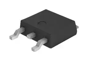
- Diode Case Style: TO-252 (DPAK)
- Diode Configuration: Single
- Forward Voltage Max: 1.3V
- Forward Surge Current: 66A
- Reverse Recovery Time: 60ns
- Average Forward Current: 5A
- Operating Temperature Max: 150°C
- Repetitive Peak Reverse Voltage: 600V
| Delivery and price | |
|---|---|
| Units per pack | 1000 |
| Price | 0.328 € |
| Current stock | 10+ |
| Lead time | 30 days |
Datasheet

**10 December 2015**

**==> picture [49 x 66] intentionally omitted <==**

## **IMPORTANT NOTICE**

## **1.  Global joint venture starts operations as WeEn Semiconductors**

Dear customer,

As from November 9th, 2015 NXP Semiconductors N.V. and Beijing JianGuang Asset Management Co. Ltd established Bipolar Power joint venture (JV), **WeEn Semiconductors** , which will be used in future Bipolar Power documents together with new contact details.

In this document where the previous NXP references remain, please use the new links as shown below.

**WWW** - For www.nxp.com use www.ween-semi.com **Email** - For salesaddresses@nxp.com use salesaddresses@ween-semi.com

For the copyright notice at the bottom of each page (or elsewhere in the document, depending on the version) “[©] **NXP Semiconductors N.V.** _**{year}**_ **. All rights reserved** ” becomes “[©] **WeEn Semiconductors Co., Ltd.** _**{year}**_ **. All rights reserved** ”

If you have any questions related to this document, please contact our nearest sales office via e- mail or phone (details via salesaddresses@ween-semi.com).

Thank you for your cooperation and understanding,

WeEn Semiconductors

**==> picture [52 x 41] intentionally omitted <==**

**==> picture [66 x 51] intentionally omitted <==**

## **BYV25D-600**

##

**Rev. 01 — 29 July 2008**

## **Product data sheet**

## **1.**

## **1.1 General description**

## **1.2 Features**

I Fast switching

- I Soft recovery characteristic

   - I Low thermal resistance

   - I High thermal cycling performance

- I Low forward voltage drop

## **1.3 Applications**

- I High frequency switched-mode power supplies

- I Discontinuous Current Mode (DCM) Power Factor Correction (PFC)

## **1.4 Quick reference data**

I VRRM ≤ 600 V I VF ≤ 1.11 V

- I IF(AV) ≤ 5 A I trr ≤ 60 ns

## **2. Pinning information**

|**2.**<br>**Pinning information**|**2.**<br>**Pinning information**|
|---|---|
|**Table 1.**<br>**Pinning**||
|**Pin**<br>**Description**<br>**Simplifed outline**<br>**Graphic symbol**||
|1<br>no connection<br>**SOT428 (DPAK)**<br>2<br>cathode (k)<br>[1]<br>3<br>anode (a)<br>mb<br>mounting base; cathode (k)<br>3<br>2<br>mb<br>1<br>k|a<br>001aaa020|


[1] It is not possible to connect to pin 2 of the SOT428 package.

**==> picture [211 x 101] intentionally omitted <==**

**BYV25D-600**

**NXP Semiconductors**

## **3. Ordering information**

## **Table 2. Ordering information**

|**Type number**|**Package**|**Package**|**Package**|
|---|---|---|---|
||**Name**|**Description**|**Version**|
|BYV25D-600|DPAK<br>plastic single-ended surface-mounted package (DPAK); 3-leads (one lead cropped)<br>SOT428|||


## **4. Limiting values**

## **Table 3. Limiting values**

In accordance with the Absolute Maximum Rating System (IEC 60134).

|**Symbol**<br>**Parameter**|**Conditions**<br>**Min**<br>**Max**<br>**Unit**|
|---|---|
|VRRM<br>repetitive peak reverse voltage|-<br>600<br>V|
|VRWM<br>crest working reverse voltage|-<br>600<br>V|
|VR<br>reverse voltage|square waveform;δ= 1.0; Tmb≤100°C<br>-<br>600<br>V|
|IF(AV)<br>average forward current|square waveform;δ= 0.5; Tmb≤131°C<br>-<br>5<br>A|
|IFRM<br>repetitive peak forward current|square waveform;δ= 0.5; Tmb≤131°C<br>-<br>10<br>A|
|IFSM<br>non-repetitive peak forward current|t = 10 ms; sinusoidal waveform<br>-<br>60<br>A|
||t = 8.3 ms; sinusoidal waveform<br>-<br>66<br>A|
|Tstg<br>storage temperature|−40<br>+150<br>°C|
|Tj<br>junction temperature|-<br>150<br>°C|


© NXP B.V. 2008. All rights reserved.

BYV25D-600_1

**Product data sheet**

**Rev. 01 — 29 July 2008**

**2 of 9**

**BYV25D-600**

**NXP Semiconductors**

## **5. Thermal characteristics**

|**Table 4.**|**Thermal characteristics**|||||||
|---|---|---|---|---|---|---|---|
|**Symbol**|**Parameter**|**Conditions**||**Min**|**Typ**|**Max**|**Unit**|
|Rth(j-mb)|thermal resistance from junction to|with heatsink compound;||-|-|3.0|K/W|
||mounting base|see<br>Figure<br>1||||||
|Rth(j-a)|thermal resistance from junction to ambient|in free air|[1]|-|50|-|K/W|


[1] Device mounted on an FR4 Printed-Circuit Board (PCB), single-sided copper, tin-plated and standard footprint.

**==> picture [233 x 149] intentionally omitted <==**

**----- Start of picture text -----**<br>
003aac235<br>10<br>Zth(j-mb)<br>(K/W)<br>1<br>10 [−][1] P δ = tp<br>T<br>10 [−][2]<br>tp t<br>T<br>10 [−][3]<br>10 [−][6] 10 [−][5] 10 [−][4] 10 [−][3] 10 [−][2] 10 [−][1] 1 10<br>tp (s)<br>**----- End of picture text -----**<br>


**Fig 1. Transient thermal impedance from junction to mounting base as a function of pulse width**

© NXP B.V. 2008. All rights reserved.

BYV25D-600_1 **Product data sheet**

**Rev. 01 — 29 July 2008**

**3 of 9**

**BYV25D-600**

**NXP Semiconductors**

## **6. Characteristics**

## **Table 5. Characteristics**

Tj = 25 °

|**Symbol**<br>**Parameter**|**Conditions**<br>**Min**<br>**Typ**<br>**Max**<br>**Unit**|
|---|---|
|**Static characteristics**||
|VF<br>forward voltage|IF= 5 A; Tj= 150°C; see<br>Figure<br>2<br>-<br>0.97<br>1.11<br>V|
||IF= 5 A<br>-<br>1.12<br>1.30<br>V|
|IR<br>reverse current|VR= 600 V<br>-<br>2<br>50<br>µA|
||VR= 600 V; Tj= 100°C<br>-<br>0.1<br>0.35<br>mA|
|**Dynamic characteristics**||
|Qr<br>recovered charge|IF= 2 A to VR≥30 V; dIF/dt = 20 A/µs;<br>see<br>Figure<br>3<br>-<br>40<br>70<br>nC|
|trr<br>reverse recovery time|IF= 1 A to VR≥30 V;<br>dIF/dt = 100 A/µs; see<br>Figure<br>3<br>-<br>50<br>60<br>ns|
|IRM<br>peak reverse recovery<br>current|IF= 10 A to VR≥30 V;<br>dIF/dt = 50 A/µs; Tj= 100°C;<br>see<br>Figure<br>3<br>-<br>3<br>5.5<br>A|
|VFR<br>forward recovery<br>voltage|IF= 10 A; dIF/dt = 10 A/µs;<br>see<br>Figure<br>4<br>-<br>3.2<br>-<br>V|


**==> picture [233 x 189] intentionally omitted <==**

**----- Start of picture text -----**<br>
003aac232<br>15<br>IF<br>(A)<br>10<br>(1) (2) (3)<br>5<br>0<br>0 0.4 0.8 1.2 1.6<br>VF (V)<br>**----- End of picture text -----**<br>


- (1) Tj = 150 °C; typical values

- (2) Tj = 150 °C; maximum values

- (3) Tj = 25 °C; maximum values

**Fig 2. Forward current as a function of forward voltage**

© NXP B.V. 2008. All rights reserved.

BYV25D-600_1

**Product data sheet**

**Rev. 01 — 29 July 2008**

**4 of 9**

**BYV25D-600**

**NXP Semiconductors**

**==> picture [497 x 227] intentionally omitted <==**

**----- Start of picture text -----**<br>
IF<br>dlF<br>IF<br>dt<br>trr<br>time<br>time<br>VF<br>10 %<br>Qr 100 % VFR<br>VF<br>IR IRM<br>001aab911 time<br>001aab912<br>Fig 3. Reverse recovery definitions Fig 4. Forward recovery definitions<br>**----- End of picture text -----**<br>


**==> picture [497 x 263] intentionally omitted <==**

**----- Start of picture text -----**<br>
003aac233 003aac234<br>10 8<br>Ptot Ptot<br>(W) δ = 1 (W)<br>8 a = 1.57<br>6<br>1.9<br>0.5<br>6 2.2<br>2.8<br>4<br>0.2<br>4.0<br>4<br>0.1<br>2<br>2<br>0 0<br>0 2 4 6 8 0 2 4 6<br>IF(AV) (A) IF(AV) (A)<br>IF(AV) = IF(RMS) × √δ a = form factor = IF(RMS) / IF(AV)<br>Fig 5. Forward power dissipation as a function of Fig 6. Forward power dissipation as a function of<br>average forward current; square waveform; average forward current; sinusoidal waveform;<br>maximum values maximum values<br>**----- End of picture text -----**<br>


© NXP B.V. 2008. All rights reserved.

BYV25D-600_1

**Product data sheet**

**Rev. 01 — 29 July 2008**

**5 of 9**

**BYV25D-600**

**NXP Semiconductors**

## **7. Package outline**

## **Plastic single-ended surface-mounted package (DPAK); 3 leads (one lead cropped) SOT428**

**==> picture [482 x 564] intentionally omitted <==**

**----- Start of picture text -----**<br>
y<br>E A A<br>b2 A1 E1<br>mounting<br>base D2<br>D1<br>HD<br>2<br>L2 L<br>1 3 L1<br>b1 b w M A c<br>e<br>e1<br>0 5 10 mm<br>scale<br>DIMENSIONS (mm are the original dimensions)<br>UNIT A A1 b b1 b2 c D1 minD2 E minE1 e e1 HD L minL1 L2 w maxy<br>2.38 0.93 0.89 1.1 5.46 0.56 6.22 6.73 10.4 2.95 0.9<br>mm 4.0 4.45 2.285 4.57 0.5 0.2 0.2<br>2.22 0.46 0.71 0.9 5.00 0.20 5.98 6.47 9.6 2.55 0.5<br>OUTLINE REFERENCES EUROPEAN<br>ISSUE DATE<br>VERSION IEC JEDEC JEITA PROJECTION<br>06-02-14<br>SOT428 TO-252 SC-63<br>06-03-16<br>**----- End of picture text -----**<br>


**Fig 7. Package outline SOT428 (TO-252)**

© NXP B.V. 2008. All rights reserved.

BYV25D-600_1

**Product data sheet**

**Rev. 01 — 29 July 2008**

**6 of 9**

**BYV25D-600**

**NXP Semiconductors**

## **8. Revision history**

|**Table 6.**|**Revision**|**history**||||
|---|---|---|---|---|---|
|**Document**|**ID**|**Release date**|**Data sheet status**|**Change notice**|**Supersedes**|
|BYV25D-600_1||20080729|Product data sheet|-|-|


© NXP B.V. 2008. All rights reserved.

BYV25D-600_1

**Product data sheet**

**Rev. 01 — 29 July 2008**

**7 of 9**

**BYV25D-600**

**NXP Semiconductors**

## **9. Legal information**

## **9.1 Data sheet status**

|**Document statu**|**s**<br>**[1]**<br>**[2]**<br>**Product status**<br>**[3]**<br>**Defnition**|
|---|---|
|Objective [short] data sheet<br>Development<br>This document contains data from the objective specifcation for product development.||
|Preliminary [short] data sheet<br>Qualifcation<br>This document contains data from the preliminary specifcation.||
|Product [short] data sheet<br>Production<br>This document contains the product specifcation.||


[1] Please consult the most recently issued document before initiating or completing a design.

[2]

[3] The product status of device(s) described in this document may have changed since this document was published and may differ in case of multiple devices. The latest product status information is available on the Internet at URL http://www.nxp.com.

## **9.2**

**Draft —** The document is a draft version only. The content is still under internal review and subject to formal approval, which may result in modifications or additions. NXP Semiconductors does not give any representations or warranties as to the accuracy or completeness of information included herein and shall have no liability for the consequences of use of such information.

**Short data sheet —** A short data sheet is an extract from a full data sheet with the same product type number(s) and title. A short data sheet is intended for quick reference only and should not be relied upon to contain detailed and full information. For detailed and full information see the relevant full data sheet, which is available on request via the local NXP Semiconductors sales office. In case of any inconsistency or conflict with the short data sheet, the full data sheet shall prevail.

## **9.3 Disclaimers**

**General —** Information in this document is believed to be accurate and reliable. However, NXP Semiconductors does not give any representations or warranties, expressed or implied, as to the accuracy or completeness of such information and shall have no liability for the consequences of use of such information.

**Right to make changes —** NXP Semiconductors reserves the right to make changes to information published in this document, including without limitation specifications and product descriptions, at any time and without notice. This document supersedes and replaces all information supplied prior to the publication hereof.

**Suitability for use —** NXP Semiconductors products are not designed, authorized or warranted to be suitable for use in medical, military, aircraft, space or life support equipment, nor in applications where failure or malfunction of an NXP Semiconductors product can reasonably be expected to result in personal injury, death or severe property or environmental

damage. NXP Semiconductors accepts no liability for inclusion and/or use of NXP Semiconductors products in such equipment or applications and therefore such inclusion and/or use is at the customer’s own risk.

**Applications —** Applications that are described herein for any of these products are for illustrative purposes only. NXP Semiconductors makes no representation or warranty that such applications will be suitable for the specified use without further testing or modification.

**Limiting values —** the Absolute Maximum Ratings System of IEC 60134) may cause permanent damage to the device. Limiting values are stress ratings only and operation of the device at these or any other conditions above those given in the Characteristics sections of this document is not implied. Exposure to limiting values for extended periods may affect device reliability.

**Terms and conditions of sale —** NXP Semiconductors products are sold subject to the general terms and conditions of commercial sale, as published at http://www.nxp.com/profile/terms, including those pertaining to warranty, intellectual property rights infringement and limitation of liability, unless explicitly otherwise agreed to in writing by NXP Semiconductors. In case of any inconsistency or conflict between information in this document and such terms and conditions, the latter will prevail.

**No offer to sell or license —** Nothing in this document may be interpreted or construed as an offer to sell products that is open for acceptance or the grant, conveyance or implication of any license under any copyrights, patents or other industrial or intellectual property rights.

**Quick reference data —** The Quick reference data is an extract of the product data given in the Limiting values and Characteristics sections of this document, and as such is not complete, exhaustive or legally binding.

## **9.4 Trademarks**

Notice: All referenced brands, product names, service names and trademarks are the property of their respective owners.

## **10. Contact information**

For more information, please visit: **http://www.nxp.com**

**salesaddresses@nxp.com**

© NXP B.V. 2008. All rights reserved.

BYV25D-600_1

**Product data sheet**

**Rev. 01 — 29 July 2008**

**8 of 9**

**BYV25D-600**

**NXP Semiconductors**

## **11. Contents**

|**11. **|**Contents**|
|---|---|
|**1**|**Product profle . . . . . . . . . . . . . . . . . . . . . . . . . .  1**|
|1.1|General description. . . . . . . . . . . . . . . . . . . . . . 1|
|1.2|Features . . . . . . . . . . . . . . . . . . . . . . . . . . . . . . 1|
|1.3|Applications  . . . . . . . . . . . . . . . . . . . . . . . . . . . 1|
|1.4|Quick reference data. . . . . . . . . . . . . . . . . . . . . 1|
|**2**|**Pinning information. . . . . . . . . . . . . . . . . . . . . .  1**|
|**3**|**Ordering information . . . . . . . . . . . . . . . . . . . . .  2**|
|**4**|**Limiting values. . . . . . . . . . . . . . . . . . . . . . . . . .  2**|
|**5**|**Thermal characteristics. . . . . . . . . . . . . . . . . . .  3**|
|**6**|**Characteristics. . . . . . . . . . . . . . . . . . . . . . . . . .  4**|
|**7**|**Package outline . . . . . . . . . . . . . . . . . . . . . . . . .  6**|
|**8**|**Revision history. . . . . . . . . . . . . . . . . . . . . . . . .  7**|
|**9**|**Legal information. . . . . . . . . . . . . . . . . . . . . . . .  8**|
|9.1|Data sheet status . . . . . . . . . . . . . . . . . . . . . . . 8|
|9.2|Defnitions. . . . . . . . . . . . . . . . . . . . . . . . . . . . . 8|
|9.3|Disclaimers . . . . . . . . . . . . . . . . . . . . . . . . . . . . 8|
|9.4|Trademarks. . . . . . . . . . . . . . . . . . . . . . . . . . . . 8|
|**10**|**Contact information. . . . . . . . . . . . . . . . . . . . . .  8**|
|**11**|**Contents . . . . . . . . . . . . . . . . . . . . . . . . . . . . . . .  9**|


**==> picture [151 x 121] intentionally omitted <==**

Please be aware that important notices concerning this document and the product(s) described herein, have been included in section ‘Legal information’.

**© NXP B.V. 2008.**

**All rights reserved.**

For more information, please visit: http://www.nxp.com For sales office addresses, please send an email to: salesaddresses@nxp.com **Date of release: 29 July 2008 Document identifier: BYV25D-600_1**
Updated at June 4, 2026
About Novapart
Novapart is a B2B electronic component broker specialising in stock shortages and cost reduction. We source hard-to-find parts and identify compliant alternatives across a catalogue of 410,000+ components from 500+ manufacturers.
Learn more →Stock Shortage Specialist
When a component is unavailable, discontinued or has an unacceptable lead time, we tap into our network of vetted European and Asian distributors to source what you need — without compromising on quality or traceability.
Request a quote →Compliant Alternatives
We identify pin-to-pin, electrically equivalent substitutes that meet the same certifications (RoHS, AEC-Q100, REACH) as your original specification — validated against datasheets, not just part numbers. Often at a lower cost.
BOM Analysis service →