


BUZ30AHXKSA1
Power MOSFET, N Channel, 200 V, 21 A, 0.1 ohm, TO-220, Through Hole
- Manufacturer: INFINEON
- Product type: Single MOSFETs
- No. of Pins: 3Pins
- Channel Type: N Channel
- Power Dissipation: 125W
- Transistor Mounting: Through Hole
- Transistor Polarity: N Channel
- Power Dissipation Pd: 125W
- Rds(on) Test Voltage: 10V
- On Resistance Rds(on): 0.1ohm
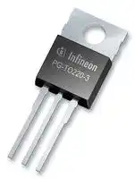
- Transistor Case Style: TO-220
- Drain Source Voltage Vds: 200V
- Operating Temperature Max: 150°C
- Continuous Drain Current Id: 21A
- Drain Source On State Resistance: 0.1ohm
- Gate Source Threshold Voltage Max: 3V
| Delivery and price | |
|---|---|
| Units per pack | 1000 |
| Price | 0.623 € |
| Current stock | 10+ |
| Lead time | 30 days |
## Cinfineon

## **SIPMOS** ® **Power Transistor**

## **BUZ 30A H**

- N channel

- Enhancement mode

- Avalanche-rated

. Halogen-free according to IEC61249-2--21

|**Pin 1**|**Pin 1**||**Pin 2**|**Pin 2**||**Pin 3**|**Pin 3**|
|---|---|---|---|---|---|---|---|
|||||||||
|G|||D|||S||


|**Maximum Ratings**||||
|---|---|---|---|
|**Parameter**|**Symbol**|**Values**|**Unit**|
|Continuous drain current<br>TC= 26 ˚C|ID<br>pp|21<br>pp|A<br>pp|
|Pulsed drain current<br>TC= 25 ˚C|IDpuls|84||
|Avalanche current,limited byTjmax|IAR<br>a|21<br> ee||
|Avalanche energy,periodic limited byTjmax|EAR|12|mJ|
|Avalanche energy, single pulse|EAS<br>Po|Po||
||Po|Po||
||Po|450<br>Po||
||VGS<br>a|±20|V|
||Ptot|125|W|
||Tj<br>a<br>pe|-55 ... + 150|˚C|
||Tstg<br>pe|-55 ... + 150||
||RthJC<br>pea|≤1|K/W|
||RthJA<br>a|75||
||aee|E<br>ee||
||a ee|55 / 150 / 56<br>ee||


Rev. 2.5                                                                    Page 1                                                2010-07-02

**BUZ 30A H**

> **Electrical Characteristics,** at Tj = 25˚C, unless otherwise specified

|Drain- source breakdown voltage<br>VGS= 0 V,ID= 0.25 mA,Tj= 25 ˚C|V(BR)DSS<br>~~|~~|200<br>~~|~~<br>|<br>||-<br>~~|~~<br>|<br>||-<br>~~|~~|V|
|---|---|---|---|---|---|
|Gate threshold voltage<br>VGS=VDS,ID= 1 mA|VGS(th)<br>~~|~~<br>tf|2.1<br>|<br>~~|~~<br>|<br>tf|3<br>|<br>~~|~~<br>|<br>tf||4<br>~~|~~<br>|||
|Zero gate voltage drain current<br>VDS= 200 V,VGS= 0 V,Tj= 25 ˚C<br>VDS= 200 V,VGS= 0 V,Tj= 125 ˚C|IDSS<br>tf|-<br>-<br>|<br>tf<br>||10<br>0.1<br>|<br>tf|<br>||100<br>1<br>||µA|
|Gate-source leakage current<br>VGS= 20 V,VDS= 0 V|IGSS<br>tf<br>||-<br>tf<br>|<br>|<br>||10<br>tf |<br>|<br>|<br>|fe|100<br>|<br>|<br>fe|nA|
|Drain-Source on-resistance<br>VGS= 10 V,ID= 13.5 A<br>||RDS(on)<br>||-<br>|<br>|<br>||0.1<br>|<br>|<br>|fe|0.13<br>|<br>fe|Ω|


Rev. 2.5                                                             Page 2                                                   2010-07-02

**BUZ 30A H**

|Transconductance<br>VDS≥2*ID *RDS(on)max,ID= 13.5 A|gfs<br>~~|~~|6<br>~~|~~<br>|<br>||15<br>~~|~~<br>|<br>||-<br>~~|~~|S|
|---|---|---|---|---|---|
|Input capacitance<br>VGS= 0 V,VDS= 25 V,f= 1 MHz|Ciss<br>~~|~~|-<br>|<br>~~|~~<br>|<br>||1400<br>|<br>~~|~~<br>|<br>||1900<br>~~|~~|pF|
|Output capacitance<br>VGS= 0 V,VDS= 25 V,f= 1 MHz|Coss<br>|||-<br>|<br>||<br>|<br>||280<br>|<br>||<br>|<br>||400<br>||||
|Reverse transfer capacitance<br>VGS= 0 V,VDS= 25 V,f= 1 MHz|Crss<br>|<br>pt|-<br>|<br>|<br>|<br>|<br>pt|130<br>|<br>|<br>|<br>|<br>|200<br>|<br>||
|Turn-on delay time<br>VDD= 30 V,VGS= 10 V,ID= 3 A<br>RGS= 50Ω|td(on)<br>et<br>pt|-<br>|<br>et<br>|<br>pt|30<br>|<br>et<br>|<br>|45<br>et<br>|ns|
|Rise time|tr<br>pt||<br>pttf||<br>tf|tf||
||pt||<br>pttf||<br>tf|tf||
||pt<br>pt|-<br>|<br>pt tf<br>|<br>pt|70<br>|<br>tf<br>|<br>|110<br>tf<br>||
||td(off)<br>pt<br>Pt<br>pt||<br>pt <br>Pt<br>|<br>pt||<br><br>Pt<br>|<br>|Pt<br>||
||Pt<br>pt|Pt<br>|<br>pt|Pt<br>|<br>|Pt<br>||
||Pt<br>pt|-<br>Pt<br>|<br>pt|250<br>Pt<br>|<br>|320<br>Pt<br>||
||tf<br>pt||<br>pttf||<br>tf|tf||
||pt||<br>pttf||<br>tf|tf||
||pt|-<br>|<br>pt tf|90<br>|<br>tf|120<br>tf||


Rev. 2.5                                                            Page 3                                                    2010-07-02

**BUZ 30A H**

**==> picture [502 x 379] intentionally omitted <==**

**----- Start of picture text -----**<br>
BUZ 30A H<br>Cinfineon<br>Electrical Characteristics,  at Tj = 25˚C, unless otherwise specified<br>Parameter Symbol Values Unit<br>min. typ. max.<br>=<br>Reverse Diode<br>Inverse diode continuous forward current IS A<br>TC = 25 ˚C - -  21<br>| |<br>Inverse diode direct current,pulsed ISM<br>TC = 25 ˚C | - | -  84<br>Inverse diode forward voltage VSD V<br>VGS = 0 V, IF = 42 A | - |  1.2 |  1.6<br>Reverse recovery time trr ns<br>VR = 100 V, IF=lS, diF/dt = 100 A/µs | - |  180 -<br>Reverse recovery charge Qrr µC<br>VR = 100 V, IF=lS, diF/dt = 100 A/µs | - |  1.2 -<br>**----- End of picture text -----**<br>


Rev. 2.5                                                                Page 4                                                2010-07-02

**BUZ 30A H**

## **Power dissipation**

Ptot =[ƒ] (TC)

## **Drain current**

ID =[ƒ] (TC) parameter: VGS[ ≥ ] 10 V

**==> picture [228 x 254] intentionally omitted <==**

**----- Start of picture text -----**<br>
130 pon EEE<br>110W POON CELA<br>P<br>tot 100 EEN TTT TTT<br>90<br>Sree<br>80<br>70<br>PCCLLTEN FAL<br>PCCALTN AL<br>60<br>50 PCELLEETLN. LE<br>40 Fit EEN Ty<br>30<br>SN<br>20<br>PECEECE ee)<br>PCCELEETATIN<br>10<br>0 POCCPPAN<br>0 20 40 60 80 100 120 ˚C 160<br>——_ > TC<br>**----- End of picture text -----**<br>


**==> picture [223 x 253] intentionally omitted <==**

**----- Start of picture text -----**<br>
22 So EEL<br>A TPE NST<br>18<br>I<br>D<br>PLT ELENEEL<br>16<br>St 14 EEE NE<br>12<br>\<br>TLTEEL TEEN EL<br>108 LTELTE ELLENLELLETN<br>6<br>CECT<br>4<br>ECC<br>2<br>0<br>FLEE EL ELE EL ELL<br>0 20 40 60 80 100 120 ˚C 160<br>T<br>a a C<br>**----- End of picture text -----**<br>


**Safe operating area** ID =[ƒ] (VDS) parameter: D = 0.01, TC = 25˚C

**Transient thermal impedance** Zth JC =[ƒ] (tp) parameter: D = tp / T

**==> picture [473 x 260] intentionally omitted <==**

**----- Start of picture text -----**<br>
10 3  10 1<br>K/W<br>A<br>eto oth 10 0  HE<br>ID 10 2  tp = 18.0µs ZthJC<br>SSSA ete ISSCC<br>10 -1<br> 100 µs<br>10 1   1 ms 10 -2<br>D = 0.50<br>0.20<br> 10 ms<br>10 -3  0.10<br>10 0  0.05<br>0.02<br>Sasa DC  10 -4  AMICUS single pulse<br>0.01<br>ar ee VV<br>10 -1  PCE CEI 10 -5  qt<br>10  [0 ] 10  [1 ] 10  [2 ] V  10  [-7 ] 10  [-6 ] 10  [-5 ] 10  [-4 ] 10  [-3 ] 10  [-2 ] 10  [-1 ] s  10  [0 ]<br>—_ VDS —_> tp<br>I D<br>  /<br>V DS<br>  =<br>R DS(on)<br>**----- End of picture text -----**<br>


Rev. 2.5                                                             Page 5                                                     2010-07-02

**BUZ 30A H**

## **Typ. output characteristics**

ID =[ƒ(] VDS) parameter: tp = 80 µs

## **Typ. drain-source on-resistance**

RDS (on) =[ƒ(] ID) parameter: VGS

**==> picture [223 x 255] intentionally omitted <==**

**----- Start of picture text -----**<br>
50<br>Ptot = 125Wtot = 125W = 125W<br>A eee l kjj i h g f<br>VGS [V] GS [V]<br>ID 40 a 4.0<br>D yee<br>ba 4.54.0<br>35 e c 5.0<br>d 5.5<br>Yo<br>30 BED) e 6.0<br>f 6.5<br>25 onan d g 7.0<br>an) Zam<br>h 7.5<br>20 i 8.0<br>c j 9.0<br>15 k 10.0<br>l 20.0<br>1055 | Zag Zag a b<br>0 Aare<br>0 2 4 6 8 V 11<br>VDS<br>DS<br>**----- End of picture text -----**<br>


**==> picture [472 x 590] intentionally omitted <==**

**----- Start of picture text -----**<br>
0.40<br>Ptot = 125Wtot = 125W = 125W a b c d e<br>A eee l kjj i h g f Ω  crcereverceenareese<br>VGS [V] GS [V]<br>ID 40 yee ba 4.54.0 RDS (on)0.32  Pope<br>35 e c 5.0 0.28<br>d 5.5<br>Yo fe<br>30 BED) e 6.0 0.24  eff dfs<br>f 6.5<br>25 onan d g 7.0 0.20  HEELEAE<br>an) Zam ars aces eeeieees<br>h 7.5<br>20 i 8.0 0.16  f<br>c j 9.0<br>g<br>15 k 10.0 0.12  h i<br>l 20.0 j k<br>l<br>b 0.08<br>VGS [V] =<br>1055 | Zag Zag a 0.04  PETE a b  TEE c d  T ETE e f  PEEP g h  Tete i j k l<br>4.0 4.5 5.0 5.5 6.0 6.5 7.0 7.5 8.0 9.0 10.0 20.0<br>0 Aare 0.00<br>0 2 4 6 8 V 11 0 4 8 12 16 20 24 28 32 A 40<br>VDS ID<br>Typ. transfer characteristics  ID = f (VGS)D = f (VGS) = f (VGS) f (VGS) (VGS)VGS)GS)) Typ. forward transconductance  gfs = f (ID)<br>parameter: tp = 80 µstp = 80 µsp = 80 µs = 80 µs parameter: tp = 80 µs,<br>DS≥2 x≥2 x2 x ID x RDS(on)maxD x RDS(on)max x RDS(on)max RDS(on)maxDS(on)max VDS≥2 x ID x RDS(on)max<br>45 20<br>S<br>A<br>TT CT] Leer<br>ID 35 gfs 16<br>14<br>30<br>t SRGeeeeeeLHL feHOARE<br>12<br>25<br>SeGee ee AS<br>10<br>20<br>SaGee teen A<br>8<br>15 Saar eeee foo<br>6<br>10 Baan nee POPE<br>4<br>5 Bae neee 2  PPP<br>0 0<br>0 1 2 3 A 4 5 LT 6 7 8 V 10 0 FE 5 10 15 20 ET 25 30 A 40<br>VGS ID<br>**----- End of picture text -----**<br>


**Typ. transfer characteristics** ID = f (VGS)D = f (VGS) = f (VGS) f (VGS) (VGS)VGS)GS)) parameter: tp = 80 µstp = 80 µsp = 80 µs = 80 µs VDS≥2 x≥2 x2 x ID x RDS(on)maxD x RDS(on)max x RDS(on)max RDS(on)maxDS(on)max

Rev. 2.5                                                               Page 6                                                    2010-07-02

**BUZ 30A H**

## **Drain-source on-resistance**

RDS (on) =[ƒ] (Tj) parameter: ID = 13.5 A, VGS = 10 V

## **Gate threshold voltage**

VGS (th) =[ƒ] (Tj) parameter: VGS = VDS, ID = 1 mA

**==> picture [482 x 255] intentionally omitted <==**

**----- Start of picture text -----**<br>
0.50 4.6<br>V<br>Ω 98%<br>TUTTE TT TT 4.0  ett<br>R 0.40 LEE EEL ELE VGS(th) 3.6  SERPS tt<br>DS (on)<br>0.35 3.2  typ<br>fe CPPPPTTTTT) BEEREERE<br>2.8<br>0.30 CPP HPP<br>2.4<br>0.25 -ECCLELEL Se 2%<br>2.0<br>0.20 tet 98% ee SE<br>1.6<br>ttt Et<br>0.15 typ<br>1.2<br>| ee EERE<br>0.10<br>tert fd 0.8  SS<br>SEPT ELLE See<br>0.05 0.4<br>0.0<br>0.00 ~ECCCELELL oe<br>-60 -20 20 60 100 ˚C 160 -60 -20 20 60 100 ˚C 160<br>—_> T Pp Tj<br>j<br>**----- End of picture text -----**<br>


## **Typ. capacitances**

C = f (VDS) parameter:VGS = 0V, f = 1MHz

**Forward characteristics of reverse diode** IF =[ƒ] (VSD) parameter: Tj, tp = 80 µs

**==> picture [470 x 258] intentionally omitted <==**

**----- Start of picture text -----**<br>
10 1 10 2<br>nF   A<br>C I<br>F<br>10 0 Ciss 10 1<br>oe Saeee e eee ee ee f K<br>Coss<br>SES COMI<br>10 -1 a Crss 10 0  SUEELEE<br>Tj = 25 ˚C typ<br>es LL PWN TTjj = 150 ˚C typ = 25 ˚C (98%) | ||<br>r | | | [ [| [| ff | [RMS Tj = 150 ˚C (98%) | [ [[|]<br>10 -2 FEEL LE 10 -1  Tl aa<br>0 5 10 15 20 25 30 V 40 0.0 0.4 0.8 1.2 1.6 2.0 2.4 V 3.0<br>er VDS —_ VSD<br>**----- End of picture text -----**<br>


Rev. 2.5                                                            Page 7                                                        2010-07-02

**BUZ 30A H**

**Avalanche energy** EAS = ƒ(Tj) parameter: ID = 21 A, VDD = 50 V RGS = 25[Ω] , L = 1.53 mH

**Typ. gate charge** VGS =[ƒ] (QGate) parameter: ID puls = 32 A

**==> picture [479 x 255] intentionally omitted <==**

**----- Start of picture text -----**<br>
500 16<br>mJ<br>EE V  HHL<br>\ 1 /|<br>EAS 400 ACLEELELLE VGS SEE<br>12<br>350<br>f SNELLONELL LLL ot 10  +++ero+64<br>300 \ P| | | 0,2 V | DS max T7Yi 0,8  tt VDS max<br>250 8<br>LENE 7<br>200 ELEN EEE Sens) 2nEen<br>6<br>150 -LELENEL ELE FEE<br>4<br>-LEELLN LEELA Ht<br>100 fi t tt ttt<br>2<br>50<br>ALLEN | [| [| | | [| | ft<br>0 PELE 0 PE<br>ELLE AKLEL CEE EL<br>20 40 60 80 100 120 ˚C 160 0 10 20 30 40 50 60 70 80 nC 100<br>Tj QGate<br>**----- End of picture text -----**<br>


**Drain-source breakdown voltage** V(BR)DSS =[ƒ] (Tj)

**==> picture [230 x 253] intentionally omitted <==**

**----- Start of picture text -----**<br>
240V PTTLPTTLELL LET LET<br>230<br>V<br>(BR)DSS<br>225<br>220<br>+ [FEET] SERS eeeeeeTy<br>PEEP<br>215 PLETELYEL A<br>210<br>205<br>200 PTT PLLA BARES?LEE45008<br>195 PIM ELL<br>190<br>185 PYLE ELLE<br>180<br>PE EEEELL ELL<br>-60 -20 20 60 100 ˚C 160<br>T<br>j<br>**----- End of picture text -----**<br>


Rev. 2.5                                                                Page 8                                                     2010-07-02

**BUZ 30A H**

## **Package Drawing: TO220-3**

2010-07-02

Page 9

Rev. 2.5

**BUZ 30A H**

**Published by Infineon Technologies AG 81726 Munich, Germany © 2010 Infineon Technologies AG All Rights Reserved.**

## **Legal Disclaimer**

The information given in this document shall in no event be regarded as a guarantee of conditions or characteristics. With respect to any examples or hints given herein, any typical values stated herein and/or any information regarding the application of the device, Infineon Technologies hereby disclaims any and all warranties and liabilities of any kind, including without limitation, warranties of non-infringement of intellectual property rights of any third party.

## **Information**

For further information on technology, delivery terms and conditions and prices, please contact the nearest Infineon Technologies Office (www.infineon.com).

## **Warnings**

Due to technical requirements, components may contain dangerous substances. For information on the types in question, please contact the nearest Infineon Technologies Office. Infineon Technologies components may be used in life-support devices or systems only with the express written approval of Infineon Technologies, if a failure of such components can reasonably be expected to cause the failure of that life-support device or system or to affect the safety or effectiveness of that device or system. Life support devices or systems are intended to be implanted in the human body or to support and/or maintain and sustain and/or protect human life. If they fail, it is reasonable to assume that the health of the user or other persons may be endangered.

Page 10

2010-07-02

Rev. 2.5
Updated at February 9, 2023
Infineon Technologies is a globally recognized leader in semiconductor solutions, renowned for driving innovation in power management, energy efficiency, and modern mobility. With a strong legacy of engineering excellence, the company provides highly reliable components designed to meet the rigorous demands of industrial, automotive, and advanced commercial applications. The core of our Infineon portfolio is centered on their industry-leading discrete semiconductors. We offer an extensive selection of single and dual MOSFETs, alongside a robust range of single IGBTs and advanced IGBT modules. These flagship power transistors are essential for high-efficiency power conversion and motor control, providing engineers with superior thermal performance and minimized switching losses. Beyond advanced field-effect transistors, the selection includes a comprehensive array of diodes and rectifiers, heavily featuring Schottky diodes, as well as fast-recovery and RF/PIN diodes. This power foundation is further supported by bipolar transistors, intelligent power modules, and thyristor SCR modules, delivering the critical building blocks required for complex power system designs. To support broader system integration, the portfolio also encompasses specialized solutions such as solid-state relays, AC/DC LED driver ICs, and Bluetooth communications modules. From high-power industrial rectifiers to wireless connectivity adapters, Infineon equips designers with the precision components needed to build efficient, scalable, and fully connected electronic systems.
About Novapart
Novapart is a B2B electronic component broker specialising in stock shortages and cost reduction. We source hard-to-find parts and identify compliant alternatives across a catalogue of 410,000+ components from 500+ manufacturers.
Learn more →Stock Shortage Specialist
When a component is unavailable, discontinued or has an unacceptable lead time, we tap into our network of vetted European and Asian distributors to source what you need — without compromising on quality or traceability.
Request a quote →Compliant Alternatives
We identify pin-to-pin, electrically equivalent substitutes that meet the same certifications (RoHS, AEC-Q100, REACH) as your original specification — validated against datasheets, not just part numbers. Often at a lower cost.
BOM Analysis service →