


BULD741T4
Bipolar (BJT) Single Transistor, NPN, 1.05 kV, 2.5 A, 30 W, TO-252 (DPAK), Surface Mount
- Manufacturer: STMICROELECTRONICS
- Product type:
- Transistor Polarity:NPN; Collector Emitter Voltage V(br)ceo:1.05kV; Transition Frequency ft:-; Power Dissipation Pd:30W; DC Collector Current:2; Available until stocks are exhausted
- MSL: MSL 1 - Unlimited
- SVHC: No SVHC (17-Dec-2015)
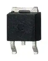
- No. of Pins: 3Pins
- Product Range: -
- Qualification: -
- Power Dissipation: 30W
- Transistor Mounting: Surface Mount
- Transistor Polarity: NPN
- Transition Frequency: -
- Transistor Case Style: TO-252 (DPAK)
- DC Current Gain hFE Min: 25hFE
- Operating Temperature Max: 150°C
- Continuous Collector Current: 2.5A
- Collector Emitter Voltage Max: 1.05kV
| Delivery and price | |
|---|---|
| Units per pack | 10 |
| Price | 0.813 € |
| Current stock | 50+ |
| Lead time | 30 days |
**BULD741**

High voltage fast-switching NPN power transistor

**==> picture [61 x 39] intentionally omitted <==**

## **Features**

- High voltage capability

- Low spread of dynamic parameters

- Minimum lot-to-lot spread for reliable operation

- Very high switching speed

## **Description**

The device is manufactured using high voltage Multi-Epitaxial Planar technology for high switching speeds and high voltage capability.

Thanks to an increased intermediate layer, it has an intrinsic ruggedness which enables the transistor to withstand an high collector current level during breakdown condition, without using the transil protection usually necessary in typical converters for lamp ballast.

## **Applications**

- Electronic ballast for fluorescent lighting

- Switch mode power supplies.

**==> picture [197 x 106] intentionally omitted <==**

**----- Start of picture text -----**<br>
3 3<br>2<br>1<br>1<br>DPAK IPAK<br>TO-252 TO-251<br>**----- End of picture text -----**<br>


## **Figure 1. Internal schematic diagram**

**==> picture [98 x 125] intentionally omitted <==**

**Table 1. Device summary**

|**Order codes**|**Marking**|**Package**|**Packaging**|
|---|---|---|---|
|BULD741T4|BULD741|DPAK|Tape & reel|
|BULD741-1|BULD741|IPAK|Tube|


1/11

July 2007

Rev 2

_www.st.com_

**Electrical ratings**

**BULD741**

## **1 Electrical ratings**

## **Table 2. Absolute maximum rating**

|**Table 2.**|**Absolute maximum rating**|||
|---|---|---|---|
|**Symbol**|**Parameter**|**Value**|**Unit**|
|VCES|Collector-emitter voltage (VBE= 0)|1050|V|
|VCEO|Collector-emitter voltage (IB= 0)|400|V|
|VEBO|Emitter-base voltage (IC= 0, IB= 2A, tP< 10ms)|V(BR)EBO|V|
|IC|Collector current|2.5|A|
|ICM|Collector peak current (tP< 5ms)|5|A|
|IB|Base current|1.5|A|
|IBM|Base peak current (tP< 5ms)|3|A|
|Ptot|Total dissipation at Tc= 25°C|30|W|
|Tstg|Storage temperature|-65 to 150|°C|
|TJ|Max. operating junction temperature|150|°C|


## **Table 3. Thermal data**

|**Table 3.**|**Thermal data**|||
|---|---|---|---|
|**Symbol**|**Parameter**|**Value**|**Unit**|
|Rthj-case|Thermal resistance junction-case__max|4.16|°C/W|


2/11

**Electrical characteristics**

**BULD741**

## **2 Electrical characteristics**

(Tcase = 25°C unless otherwise specified)

## **Table 4. Electrical characteristics**

|**Symbol**|**Parameter**|**Test conditions**|**Min.**|**Typ.**|**Max.**|**Unit**|
|---|---|---|---|---|---|---|
|ICES|Collector cut-off current<br>(VBE=0V)|VCE=1050V||0.2|10|µA|
|ICEO|Collector cut-off current<br>(IB=0)|VCE=400V||10|250|µA|
|V(BR)EBO|Emitter-base breakdown<br>voltage (IC= 0)|IE=1mA|15|19|24|V|
|VCEO(sus)<br>(1)|Collector-emitter<br>sustaining voltage<br>(IB= 0)|IC=10mA|400|450||V|
|VCE(sat)<br>(1)|Collector-emitter<br>saturation voltage|IC=0.7A              IB=0.14A<br>IC=2A                 IB=0.6A||0.15<br>0.5|0.5<br>1.5|V<br>V|
|VBE(sat)<br>(1)|Base-emitter saturation<br>voltage|IC=2A                 IB=0.6A||1.1|1.5|V|
|hFE|DC current gain|IC=0.1A             VCE=5V<br>IC=0.45A           VCE=3V|48<br>25|70<br>35|100<br>50||
|ts<br>tf|Resistive load<br>Storage time<br>Fall time|VCC=125V         IC=1A<br>IB1= -IB2=0.2A   tp= 300µs<br>VBE(off)=-5V||2.5<br>350|3.5<br>500|µs<br>ns|
|Ear|Repetitive avalanche<br>energy|L =2mH              C =1.8nF<br>VBE(off)=-5V|5|||mJ|


Note (1) Pulsed duration = 300 µ s, duty cycle ≤ 1.5%

3/11

**Electrical characteristics**

**BULD741**

## **2.1 Electrical characteristics (curves)**

**Figure 2. Safe operating area**

## **Figure 3. Derating curve**

**==> picture [138 x 137] intentionally omitted <==**

**==> picture [138 x 139] intentionally omitted <==**

**Figure 4. Output characteristics**

**==> picture [141 x 134] intentionally omitted <==**

**Figure 5. Reverse biased safe operating area**

**==> picture [142 x 140] intentionally omitted <==**

**Figure 6. DC current gain**

**Figure 7. DC current gain**

**==> picture [138 x 140] intentionally omitted <==**

**==> picture [138 x 140] intentionally omitted <==**

4/11

**Electrical characteristics**

**BULD741**

## **Figure 8. Base-emitter saturation Figure 9. Collector-emitter saturation voltage voltage**

**==> picture [146 x 139] intentionally omitted <==**

**==> picture [138 x 135] intentionally omitted <==**

## **Figure 10. Resistive load switching on times**

**==> picture [142 x 138] intentionally omitted <==**

## **Figure 11. Resistive load switching on times**

**==> picture [144 x 140] intentionally omitted <==**

**Figure 12. Resistive load switching off times**

**==> picture [141 x 138] intentionally omitted <==**

## **Figure 13. Resistive load switching off times**

**==> picture [142 x 138] intentionally omitted <==**

5/11

**Electrical characteristics**

**BULD741**

## **2.2 Test circuits**

**==> picture [405 x 182] intentionally omitted <==**

**----- Start of picture text -----**<br>
Figure 14. Resistive load switching test circuit<br>1) Fast electronic switch<br>2) Non-inductive resistor<br>**----- End of picture text -----**<br>


## **Figure 15. Energy rating test circuit**

**==> picture [217 x 159] intentionally omitted <==**

6/11

**Package mechanical data**

**BULD741**

## **3 Package mechanical data**

In order to meet environmental requirements, ST offers these devices in ECOPACK® packages. These packages have a Lead-free second level interconnect. The category of second level interconnect is marked on the package and on the inner box label, in compliance with JEDEC Standard JESD97. The maximum ratings related to soldering conditions are also marked on the inner box label. ECOPACK is an ST trademark. ECOPACK specifications are available at: www.st.com

7/11

**Package mechanical data**

**BULD741**

||||||||||**inch**<br>**MAX.**<br>**MIN.**<br>**TYP.**<br>**MAX.**<br>2.40<br>0.087<br>0.094<br>1.10<br>0.035<br>0.043<br>0.23<br>0.001<br>0.009<br>0.90<br>0.025<br>0.035<br>5.40<br>0.204<br>0.213<br>0.60<br>0.018<br>0.024<br>0.60<br>0.019<br>0.024<br>6.20<br>0.236<br>0.244<br>6.60<br>0.252<br>0.260<br>4.60<br>0.173<br>0.181<br>10.10<br>0.368<br>0.398<br>0.031<br>1.00<br>0.024<br>0.039<br>8o<br>0o<br>0o<br>P032P_B<br>**) MECHANICAL DATA**|**inch**<br>**MAX.**<br>**MIN.**<br>**TYP.**<br>**MAX.**<br>2.40<br>0.087<br>0.094<br>1.10<br>0.035<br>0.043<br>0.23<br>0.001<br>0.009<br>0.90<br>0.025<br>0.035<br>5.40<br>0.204<br>0.213<br>0.60<br>0.018<br>0.024<br>0.60<br>0.019<br>0.024<br>6.20<br>0.236<br>0.244<br>6.60<br>0.252<br>0.260<br>4.60<br>0.173<br>0.181<br>10.10<br>0.368<br>0.398<br>0.031<br>1.00<br>0.024<br>0.039<br>8o<br>0o<br>0o<br>P032P_B<br>**) MECHANICAL DATA**|**inch**<br>**MAX.**<br>**MIN.**<br>**TYP.**<br>**MAX.**<br>2.40<br>0.087<br>0.094<br>1.10<br>0.035<br>0.043<br>0.23<br>0.001<br>0.009<br>0.90<br>0.025<br>0.035<br>5.40<br>0.204<br>0.213<br>0.60<br>0.018<br>0.024<br>0.60<br>0.019<br>0.024<br>6.20<br>0.236<br>0.244<br>6.60<br>0.252<br>0.260<br>4.60<br>0.173<br>0.181<br>10.10<br>0.368<br>0.398<br>0.031<br>1.00<br>0.024<br>0.039<br>8o<br>0o<br>0o<br>P032P_B<br>**) MECHANICAL DATA**|**inch**<br>**MAX.**<br>**MIN.**<br>**TYP.**<br>**MAX.**<br>2.40<br>0.087<br>0.094<br>1.10<br>0.035<br>0.043<br>0.23<br>0.001<br>0.009<br>0.90<br>0.025<br>0.035<br>5.40<br>0.204<br>0.213<br>0.60<br>0.018<br>0.024<br>0.60<br>0.019<br>0.024<br>6.20<br>0.236<br>0.244<br>6.60<br>0.252<br>0.260<br>4.60<br>0.173<br>0.181<br>10.10<br>0.368<br>0.398<br>0.031<br>1.00<br>0.024<br>0.039<br>8o<br>0o<br>0o<br>P032P_B<br>**) MECHANICAL DATA**|
|---|---|---|---|---|---|---|---|---|---|---|---|---|
|||||||**T**|**O-252 (DPAK**||**) MECHANICAL DATA**||||
||||||||||||||
|||**DIM**||||||**mm**|||**inch**||
|||**.**|||**MI**|**N.**||**TYP.**|**MAX**|**.**<br>**M**|**IN.**<br>**TYP.**|**MAX.**|
|||A|||2.2|0|||2.40|0.|087|0.094|
|||A1|||0.9|0|||1.10|0.|035|0.043|
|||A2|||0.0|3|||0.23|0.|001|0.009|
|||B|||0.6|4|||0.90|0.|025|0.035|
|||B2|||5.2|0|||5.40|0.|204|0.213|
|||C|||0.4|5|||0.60|0.|018|0.024|
|||C2|||0.4|8|||0.60|0.|019|0.024|
|||D|||6.0|0|||6.20|0.|236|0.244|
|||E|||6.4|0|||6.60|0.|252|0.260|
|||G|||4.4|0|||4.60|0.|173|0.181|
|||H|||9.3|5|||10.1|0<br>0.|368|0.398|
|||L2||||||0.8|||0.031||
|||L4|||0.6|0|||1.00|0.|024|0.039|
|||V2|||0o||||8o|0|o|0o|
||||||||||||||
||||||||||||P032P_B||
||||||||||||||
||||||||||||||
||||||||||||||
||||||||||||||
||||||||||||||
||||||||||||||
||||||||||||||
||||||||||||||
||||||||||||||


8/11

**Package mechanical data**

**BULD741**

## **TO-251 (IPAK) MECHANICAL DATA**

|**DIM**|**mm**|**mm**|**mm**|**inch**|**inch**|**inch**|
|---|---|---|---|---|---|---|
|**.**|**MIN.**|**TYP.**|**MAX.**|**MIN.**|**TYP.**|**MAX.**|
|A|2.20||2.40|0.087||0.094|
|A1|0.90||1.10|0.035||0.043|
|A3|0.70||1.30|0.028||0.051|
|B|0.64||0.90|0.025||0.035|
|B2|5.20||5.40|0.204||0.213|
|B3|||0.85|||0.033|
|B5||0.30|||0.012||
|B6|||0.95|||0.037|
|C|0.45||0.60|0.018||0.024|
|C2|0.48||0.60|0.019||0.024|
|D|6.00||6.20|0.237||0.244|
|E|6.40||6.60|0.252||0.260|
|G|4.40||4.60|0.173||0.181|
|H|15.90||16.30|0.626||0.642|
|L|9.00||9.40|0.354||0.370|
|L1|0.80||1.20|0.031||0.047|
|L2||0.80|1.00||0.031|0.039|
|V1||10o|||10o||


**==> picture [230 x 209] intentionally omitted <==**

**==> picture [32 x 8] intentionally omitted <==**

**----- Start of picture text -----**<br>
P032N_E<br>**----- End of picture text -----**<br>


9/11

**Revision history**

**BULD741**

## **4 Revision history**

**Table 5. Revision history**

|**Date**|**Revision**|**Changes**|
|---|---|---|
|20-Dec-2006|1|Initial release.|
|09-Jul-2007|2|Updated package names in page 1, added figure 4, updated<br>figure 12 and 13.|


10/11

**BULD741**

## **Please Read Carefully:**

Information in this document is provided solely in connection with ST products. STMicroelectronics NV and its subsidiaries (“ST”) reserve the right to make changes, corrections, modifications or improvements, to this document, and the products and services described herein at any time, without notice.

All ST products are sold pursuant to ST’s terms and conditions of sale.

Purchasers are solely responsible for the choice, selection and use of the ST products and services described herein, and ST assumes no liability whatsoever relating to the choice, selection or use of the ST products and services described herein.

No license, express or implied, by estoppel or otherwise, to any intellectual property rights is granted under this document. If any part of this document refers to any third party products or services it shall not be deemed a license grant by ST for the use of such third party products or services, or any intellectual property contained therein or considered as a warranty covering the use in any manner whatsoever of such third party products or services or any intellectual property contained therein.

**UNLESS OTHERWISE SET FORTH IN ST’S TERMS AND CONDITIONS OF SALE ST DISCLAIMS ANY EXPRESS OR IMPLIED WARRANTY WITH RESPECT TO THE USE AND/OR SALE OF ST PRODUCTS INCLUDING WITHOUT LIMITATION IMPLIED WARRANTIES OF MERCHANTABILITY, FITNESS FOR A PARTICULAR PURPOSE (AND THEIR EQUIVALENTS UNDER THE LAWS OF ANY JURISDICTION), OR INFRINGEMENT OF ANY PATENT, COPYRIGHT OR OTHER INTELLECTUAL PROPERTY RIGHT.**

**UNLESS EXPRESSLY APPROVED IN WRITING BY AN AUTHORIZE REPRESENTATIVE OF ST, ST PRODUCTS ARE NOT RECOMMENDED, AUTHORIZED OR WARRANTED FOR USE IN MILITARY, AIR CRAFT, SPACE, LIFE SAVING, OR LIFE SUSTAINING APPLICATIONS, NOR IN PRODUCTS OR SYSTEMS, WHERE FAILURE OR MALFUNCTION MAY RESULT IN PERSONAL INJURY, DEATH, OR SEVERE PROPERTY OR ENVIRONMENTAL DAMAGE. ST PRODUCTS WHICH ARE NOT SPECIFIED AS “AUTOMOTIVE GRADE” MAY ONLY BE USED IN AUTOMOTIVE APPLICATIONS AT USER’S OWN RISK.**

Resale of ST products with provisions different from the statements and/or technical features set forth in this document shall immediately void any warranty granted by ST for the ST product or service described herein and shall not create or extend in any manner whatsoever, any liability of ST.

ST and the ST logo are trademarks or registered trademarks of ST in various countries.

Information in this document supersedes and replaces all information previously supplied.

The ST logo is a registered trademark of STMicroelectronics. All other names are the property of their respective owners.

© 2007 STMicroelectronics - All rights reserved

STMicroelectronics group of companies

Australia - Belgium - Brazil - Canada - China - Czech Republic - Finland - France - Germany - Hong Kong - India - Israel - Italy - Japan - Malaysia - Malta - Morocco - Singapore - Spain - Sweden - Switzerland - United Kingdom - United States of America

**www.st.com**

11/11
Updated at April 27, 2026
STMicroelectronics is a global leader in the semiconductor industry, recognized for developing highly integrated, energy-efficient solutions that power modern electronics. With a strong focus on innovation, ST provides a comprehensive portfolio of microelectronics that address the demanding requirements of industrial, automotive, communications, and consumer applications. Our extensive selection of STMicroelectronics components is built around a robust lineup of discrete semiconductors and circuit protection devices. We offer a wide variety of single MOSFETs, Schottky diodes, and fast and ultrafast recovery rectifier diodes, designed to deliver exceptional efficiency and thermal performance in power management and conversion systems. For robust circuit protection, our inventory features hundreds of transient voltage suppressors and TVS diodes that safeguard sensitive electronic components against destructive voltage spikes. In addition to core power discretes like TRIACs, SCRs, bipolar transistors, and single IGBTs, our STMicroelectronics range includes specialized integrated passive filters and MEMS sensors. Furthermore, ST offers advanced integrated passive devices, such as baluns and RF filters, which utilize high-quality monolithic RF IPD processes on glass or high-resistance silicon substrates. These components provide competitive cost structures, reduced power losses, and simplified RFIC-to-antenna matching, ensuring optimal system performance and delivering the reliability required for next-generation wireless and power designs.
About Novapart
Novapart is a B2B electronic component broker specialising in stock shortages and cost reduction. We source hard-to-find parts and identify compliant alternatives across a catalogue of 410,000+ components from 500+ manufacturers.
Learn more →Stock Shortage Specialist
When a component is unavailable, discontinued or has an unacceptable lead time, we tap into our network of vetted European and Asian distributors to source what you need — without compromising on quality or traceability.
Request a quote →Compliant Alternatives
We identify pin-to-pin, electrically equivalent substitutes that meet the same certifications (RoHS, AEC-Q100, REACH) as your original specification — validated against datasheets, not just part numbers. Often at a lower cost.
BOM Analysis service →