
Image not available
Illustrative purposes only

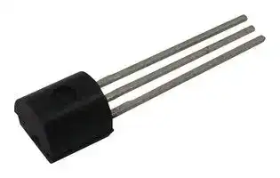
BUJ100LR,412
Bipolar (BJT) Single Transistor, NPN, 400 V, 1 A, 2.1 W, SOT-54, Through Hole
⚠️ Reference pricing provided. In case of supply shortages, we will connect you with our trusted procurement partners to ensure your project's continuity.
- Manufacturer: WEEN SEMICONDUCTORS
- Product type: Single Bipolar Junction Transistors - BJT
- No. of Pins: 3Pins
- Power Dissipation: 2.1W
- DC Current Gain hFE: 7.5hFE
- Transistor Mounting: Through Hole
- Transistor Polarity: NPN
- Transistor Case Style: SOT-54
- DC Current Gain hFE Min: 7.5hFE
- Operating Temperature Max: 150°C
- Continuous Collector Current: 1A
- Collector Emitter Voltage Max: 400V
| Delivery and price | |
|---|---|
| Units per pack | 1 |
| Price | 0.029 € |
| Current stock | 10+ |
| Lead time | 30 days |
Datasheet

## **BUJ100LR**

## **NPN power transistor**

**Rev. 02 — 29 July 2010**

## **Product data sheet**

## **1. Product profile**

## **1.1 General description**

High voltage, high speed, planar passivated NPN power switching transistor in a SOT54 (TO-92) 3 leads plastic package.

## **1.2 Features and benefits**

- Fast switching

- High voltage capability of 700 V

## **1.3 Applications**

- Compact fluorescent lamps (CFL)

- Electronic lighting ballasts

- Inverters

- Off-line self-oscillating power supplies

## **1.4 Quick reference data**

## **Table 1. Quick reference data**

|**Symbol**|**Parameter**|**Conditions**|**Min**|**Typ**|**Max**|**Unit**|
|---|---|---|---|---|---|---|
|IC|collector current|DC; seeFigure 2|-|-|1|A|
||||||||
|Ptot|total power|Tlead≤25 °C; seeFigure 1|-|-|2.1|W|
||dissipation||||||
|VCESM|collector-emitter peak|VBE= 0 V|-|-|700|V|
||voltage||||||
|**Static characteristics**|||||||
|hFE|DC current gain|VCE= 5 V; IC= 0.8 A;|5|7.5|20||
|||Tlead= 25 °C; seeFigure 8<br>;|||||
|||seeFigure 9|||||


**==> picture [172 x 101] intentionally omitted <==**

**BUJ100LR**

**NXP Semiconductors**

**NPN power transistor**

## **2. Pinning information**

## **Table 2. Pinning information**

|**Pin**|**Symbol**|**Description**|**Simplified outline**|**Simplified outline**|**Simplified outline**|**Simplified outline**|**Simplified outline**|**Simplified outline**|**Simplified outline**|**Simplified outline**|**Simplified outline**|**Simplified outline**|**Graphic symbol**|||
|---|---|---|---|---|---|---|---|---|---|---|---|---|---|---|---|
|1|B|base||||||||||||||
|2|C|collector|||||||||||||C|
|3|E|emitter|||||||||||B|||
||||||||||||||||E|
|||||1<br>2<br>3||||||||||_sym123_||
||||**SOT54**||||**(TO-92)**|||||||||


## **3. Ordering information**

## **Table 3. Ordering information**

|**Type number**|**Package**|
|---|---|
||**Name**<br>**Description**<br>**Version**|
|BUJ100LR|TO-92<br>plastic single-ended leaded (through hole) package; 3 leads<br>SOT54|


## **4. Limiting values**

## **Table 4. Limiting values**

_In accordance with the Absolute Maximum Rating System (IEC 60134)._

|**Symbol**|**Parameter**|**Conditions**|**Min**|**Max**|**Unit**|
|---|---|---|---|---|---|
|VCESM|collector-emitter peak voltage|VBE= 0 V|-|700|V|
|VCBO|collector-base voltage|IE= 0 A|-|700|V|
|VCEO|collector-emitter voltage|IB= 0 A|-|400|V|
|IC|collector current|DC; seeFigure 2|-|1|A|
|||||||
|ICM|peak collector current||-|2|A|
|IB|base current|DC|-|0.5|A|
|IBM|peak base current||-|1|A|
|Ptot|total power dissipation|Tlead≤25 °C; see Figure 1|-|2.1|W|
|Tstg|storage temperature||-65|150|°C|
|Tj|junction temperature||-|150|°C|
|VEBO|emitter-base voltage|IC= 0 A; I(Emitter) = 10 mA|-|9|V|


© NXP B.V. 2010. All rights reserved.

All information provided in this document is subject to legal disclaimers.

BUJ100LR

**Product data sheet**

**Rev. 02 — 29 July 2010**

**2 of 12**

**BUJ100LR**

**NXP Semiconductors**

**NPN power transistor**

**==> picture [190 x 186] intentionally omitted <==**

**----- Start of picture text -----**<br>
003aae644<br>120<br>Pder<br>(%)<br>80 IN TTT<br>40<br>0<br>0 50 100 150 200<br>Tlead (°C)<br>**----- End of picture text -----**<br>


## **Fig 1. Normalized total power dissipation as a function of lead temperature**

**==> picture [446 x 188] intentionally omitted <==**

**----- Start of picture text -----**<br>
003aad545<br>10 [2]<br>IC<br>————$—— ee<br>(A) fp t—“—~tSSC(;‘CSCS;CésrSC“‘(SS*ésSTSCS ST<br>10 a eee<br>——————$_—— | = = = e e e<br>po<br>IC(max) 1 a————_——_— eeeee ee<br>}—_____| fret|.  — — - -<br>10 [−][1] ee<< eee<br>Pf e (1) e<br>10 [−][2] a  fee et ee eee ee ee<br>DC<br>=<br>10 [−][3] PE EE<br>1 10 10 [2] 10 [3]<br>VCL(CE) (V)<br>**----- End of picture text -----**<br>


**Fig 2. Forward bias safe operating area**

© NXP B.V. 2010. All rights reserved.

All information provided in this document is subject to legal disclaimers.

BUJ100LR

**Product data sheet**

**Rev. 02 — 29 July 2010**

**3 of 12**

**BUJ100LR**

**NXP Semiconductors**

**NPN power transistor**

## **5. Thermal characteristics**

## **Table 5. Thermal characteristics**

**==> picture [497 x 305] intentionally omitted <==**

**----- Start of picture text -----**<br>
Symbol Parameter Conditions Min Typ Max Unit<br>Rth(j-lead) thermal resistance from  see Figure 3 - - 60 K/W<br>junction to lead<br>Rth(j-a) thermal resistance from  printed-circuit board mounted; lead  - 150 - K/W<br>junction to ambient length 4 mm<br>001aab451<br>10 [2]<br>Zth(j-lead)<br>(K/W)<br>10<br>1<br>P δ = tp<br>T<br>10 [−][1]<br>tp t<br>T<br>10 [−][2]<br>10 [−][5] 10 [−][4] 10 [−][3] 10 [−][2] 10 [−][1] 1 10<br>tp (s)<br>Fig 3. Transient thermal impedance from junction to lead as a function of pulse width<br>**----- End of picture text -----**<br>


© NXP B.V. 2010. All rights reserved.

All information provided in this document is subject to legal disclaimers.

BUJ100LR

**Product data sheet**

**Rev. 02 — 29 July 2010**

**4 of 12**

**BUJ100LR**

**NXP Semiconductors**

**NPN power transistor**

## **6. Characteristics**

|**Table 6.**<br>**Characteristics**||
|---|---|
|**Symbol**<br>**Parameter**|**Conditions**<br>**Min**<br>**Typ**<br>**Max**<br>**Unit**|
|**Static characteristics**||
|ICES<br>collector-emitter cut-off<br>current|VBE= 0 V; VCE= 700 V; Tj= 125 °C<br>-<br>-<br>5<br>mA|
|IEBO<br>emitter-base cut-off<br>current|VEB= 9 V; IC= 0 A; Tlead= 25 °C<br>-<br>-<br>1<br>mA|
|VCEOsus<br>collector-emitter<br>sustaining voltage|IB= 0 A; IC= 1 mA; LC= 25 mH;<br>Tlead= 25 °C; seeFigure 4<br>;see Figure 5<br>400<br>-<br>-<br>V|
|VCEsat<br>collector-emitter<br>saturation voltage|IC= 0.25 A; IB= 50 mA; Tlead= 25 °C;<br>seeFigure 6<br>-<br>0.2<br>0.5<br>V|
||IC= 0.5 A; IB= 125 mA; Tlead= 25 °C;<br>seeFigure 6<br>-<br>0.3<br>1<br>V|
||IC= 0.75 A; IB= 250 mA; Tlead= 25 °C;<br>seeFigure 6<br>-<br>0.4<br>1.5<br>V|
|VBEsat<br>base-emitter saturation<br>voltage|IC= 0.25 A; IB= 50 mA; Tlead= 25 °C;<br>seeFigure 7<br>-<br>-<br>1<br>V|
||IC= 0.5 A; IB= 125 mA; Tlead= 25 °C;<br>seeFigure 7<br>-<br>-<br>1.2<br>V|
|hFE<br>DC current gain|IC= 0.5 mA; VCE= 2 V; Tlead= 25 °C<br>12<br>-<br>-|
||IC= 0.4 A; VCE= 5 V; Tlead= 25 °C;<br>seeFigure 8<br>;seeFigure 9<br>10<br>-<br>30|
||IC= 0.8 A; VCE= 5 V; Tlead= 25 °C;<br>seeFigure 8<br>;seeFigure 9<br>5<br>7.5<br>20|
|**Dynamic characteristics**||
|tf<br>fall time|IC= 1 A; IBon= 200 mA; VBB= -5 V;<br>LB= 1 µH; Tlead= 25 °C; inductive load;<br>seeFigure 10<br>;seeFigure 11<br>-<br>80<br>-<br>ns|


**==> picture [497 x 217] intentionally omitted <==**

**----- Start of picture text -----**<br>
50 V IC<br>100 Ω to 200 Ω (mA)<br>horizontal<br>oscilloscope<br>vertical 250<br>6 V<br>300 Ω 1 Ω<br>100<br>30 Hz to 60 Hz<br>001aab987<br>10<br>0<br>min VCE (V)<br>VCEOsus<br>001aab988<br>Fig 4. Test circuit for collector-emitter sustaining  Fig 5. Oscilloscope display for collector-emitter<br>voltage sustaining voltage test waveform<br>**----- End of picture text -----**<br>


© NXP B.V. 2010. All rights reserved.

All information provided in this document is subject to legal disclaimers.

BUJ100LR **Product data sheet**

**Rev. 02 — 29 July 2010**

**5 of 12**

**BUJ100LR**

**NXP Semiconductors**

**NPN power transistor**

**==> picture [439 x 186] intentionally omitted <==**

**----- Start of picture text -----**<br>
003aad548 003aad549<br>2.0 1.6<br>VBEsat TI<br>VCEsat HEH Tj = 125 °C (V) co coo<br>(V)1.6 all! 1.4 i0<br>| Tj = 25 °C 1.2 ee Tj =  Celie” −35 °C  CT<br>1.2 i i 1.0 am Tj = 25   aniill °C  Zaeeilll<br>a Tj = −35 °C Va 0.8 cpenfinee mmeent<br>0.8 ei Ga seman Tj = 125 °C TT<br>0.6<br>COHNCO 1 S oe<br>na a E A<br>0.4<br>0.4 a ey) il ns 0<br>CT AhY 0.2 St<br>0 Seer [adele)] _fY 0 oon Coon in<br>10 [−][2] 10 [−][1] 1 10 10 [−][2] 10 [−][1] 1 10<br>IC (A) IC (A)<br>**----- End of picture text -----**<br>


**Fig 6. Collector-emitter saturation voltage as a function of collector current; typical values**

**Fig 7. Base-emitter saturation voltage as a function of collector current; typical values**

**==> picture [433 x 186] intentionally omitted <==**

**----- Start of picture text -----**<br>
003aad546 003aad547<br>10 [2] 10 [2]<br>EE EH<br>=H Tj = 125 °C EHHFrc Tj = 125 °C<br>Fee ee. TI ee EI UICC<br>hFE hFE<br>eet CTT ee<br>St Tj = 25 °C Tj = −35 °C Ni TER Tj = 25 °C Tj = −35 °C se<br>10 Soca NIL 10 ou<br>fy cay ENT IIll tp cumbe I N LL<br>CPeeIee, (emCTI Se RN eat eee<br>SA VCE = 3 V (1) il SH VCE = 5 V (1) il<br>(2) (2)<br>(3) (3)<br>1 1<br>10 [−][3] 10 [−][2] 10 [−][1] 1 10 10 [−][3] 10 [−][2] 10 [−][1] 1 10<br>IC (A) IC (A)<br>**----- End of picture text -----**<br>


**Fig 8. DC current gain as a function of collector current; typical values**

**Fig 9. DC current gain as a function of collector current; typical values**

© NXP B.V. 2010. All rights reserved.

All information provided in this document is subject to legal disclaimers. **Rev. 02 — 29 July 2010**

BUJ100LR

**Product data sheet**

**6 of 12**

**BUJ100LR**

**NXP Semiconductors**

**NPN power transistor**

**==> picture [478 x 245] intentionally omitted <==**

**----- Start of picture text -----**<br>
VCC IC<br>ICon<br>90 %<br>LC<br>IBon LB<br>DUT<br>VBB<br>001aab991<br>10 %<br>t<br>~ tf<br>ts<br>Veco = 300 Vi Vag = —5 Vi Le= 200 pH; Lp = 1pH IB ae toff<br>IBon<br>t<br>−IBoff<br>001aab992<br>Fig 10. Test circuit for inductive load switching Fig 11. Switching times waveforms for inductive load<br>**----- End of picture text -----**<br>


© NXP B.V. 2010. All rights reserved.

All information provided in this document is subject to legal disclaimers. **Rev. 02 — 29 July 2010**

BUJ100LR **Product data sheet**

**7 of 12**

**BUJ100LR**

**NXP Semiconductors**

**NPN power transistor**

## **7. Package outline**

**==> picture [475 x 10] intentionally omitted <==**

**----- Start of picture text -----**<br>
Plastic single-ended leaded (through hole) package; 3 leads SOT54<br>**----- End of picture text -----**<br>


**==> picture [478 x 570] intentionally omitted <==**

**----- Start of picture text -----**<br>
c<br>E<br>d A L<br>b<br>1<br>e1<br>2<br>D e<br>3<br>b1 L1<br>0 2.5 5 mm<br>scale<br>DIMENSIONS (mm are the original dimensions)<br>UNIT A b b1 c D d E e e1 L Lmax.1 [(1)]<br>5.2 0.48 0.66 0.45 4.8 1.7 4.2 14.5<br>mm 2.54 1.27 2.5<br>5.0 0.40 0.55 0.38 4.4 1.4 3.6 12.7<br>Note<br>1. Terminal dimensions within this zone are uncontrolled to allow for flow of plastic and terminal irregularities.<br>OUTLINE  REFERENCES EUROPEAN<br>ISSUE DATE<br>VERSION  IEC  JEDEC  JEITA PROJECTION<br>04-06-28<br> SOT54 TO-92 SC-43A<br>04-11-16<br>**----- End of picture text -----**<br>


## **Fig 12. Package outline SOT54 (TO-92)**

BUJ100LR

All information provided in this document is subject to legal disclaimers.

© NXP B.V. 2010. All rights reserved.

**Product data sheet**

**Rev. 02 — 29 July 2010**

**8 of 12**

**BUJ100LR**

**NXP Semiconductors**

**NPN power transistor**

## **8. Revision history**

|**Table 7.**|**Revision**|**history**||||
|---|---|---|---|---|---|
|**Document**|**ID**|**Release date**|**Data sheet status**|**Change notice**|**Supersedes**|
|BUJ100LR|v.2|20100729|Product data sheet|-|BUJ100LR v.1|
|Modifications:||**•** Various changes to content.||||
|BUJ100LR|v.1|20090812|Product data sheet|-|-|


© NXP B.V. 2010. All rights reserved.

All information provided in this document is subject to legal disclaimers. **Rev. 02 — 29 July 2010**

BUJ100LR

**Product data sheet**

**9 of 12**

**BUJ100LR**

**NXP Semiconductors**

**NPN power transistor**

## **9. Legal information**

## **9.1 Data sheet status**

|**Document status[1]**<br>**[2]**|**Product status[3]**|**Definition**|
|---|---|---|
|Objective [short] data sheet|Development|This document contains data from the objective specification for product development.|
|Preliminary [short] data sheet|Qualification|This document contains data from the preliminary specification.|
|Product [short] data sheet|Production|This document contains the product specification.|


[1] Please consult the most recently issued document before initiating or completing a design.

[2] The term 'short data sheet' is explained in section "Definitions".

[3] The product status of device(s) described in this document may have changed since this document was published and may differ in case of multiple devices. The latest product status information is available on the Internet at URL http://www.nxp.com.

## **9.2 Definitions**

**Draft** — The document is a draft version only. The content is still under internal review and subject to formal approval, which may result in modifications or additions. NXP Semiconductors does not give any representations or warranties as to the accuracy or completeness of information included herein and shall have no liability for the consequences of use of such information.

**Short data sheet** — A short data sheet is an extract from a full data sheet with the same product type number(s) and title. A short data sheet is intended for quick reference only and should not be relied upon to contain detailed and full information. For detailed and full information see the relevant full data sheet, which is available on request via the local NXP Semiconductors sales office. In case of any inconsistency or conflict with the short data sheet, the full data sheet shall prevail.

**Product specification** — The information and data provided in a Product data sheet shall define the specification of the product as agreed between NXP Semiconductors and its customer, unless NXP Semiconductors and customer have explicitly agreed otherwise in writing. In no event however, shall an agreement be valid in which the NXP Semiconductors product is deemed to offer functions and qualities beyond those described in the Product data sheet.

## **9.3 Disclaimers**

**Limited warranty and liability** — Information in this document is believed to be accurate and reliable. However, NXP Semiconductors does not give any representations or warranties, expressed or implied, as to the accuracy or completeness of such information and shall have no liability for the consequences of use of such information.

In no event shall NXP Semiconductors be liable for any indirect, incidental, punitive, special or consequential damages (including - without limitation - lost profits, lost savings, business interruption, costs related to the removal or replacement of any products or rework charges) whether or not such damages are based on tort (including negligence), warranty, breach of contract or any other legal theory.

Notwithstanding any damages that customer might incur for any reason whatsoever, NXP Semiconductors’ aggregate and cumulative liability towards customer for the products described herein shall be limited in accordance with the _Terms and conditions of commercial sale_ of NXP Semiconductors.

**Right to make changes** — NXP Semiconductors reserves the right to make changes to information published in this document, including without limitation specifications and product descriptions, at any time and without notice. This document supersedes and replaces all information supplied prior to the publication hereof.

**Suitability for use** — NXP Semiconductors products are not designed, authorized or warranted to be suitable for use in medical, military, aircraft, space or life support equipment, nor in applications where failure or malfunction of an NXP Semiconductors product can reasonably be expected to result in personal injury, death or severe property or environmental damage. NXP Semiconductors accepts no liability for inclusion and/or use of NXP Semiconductors products in such equipment or applications and therefore such inclusion and/or use is at the customer’s own risk.

**Applications** — Applications that are described herein for any of these products are for illustrative purposes only. NXP Semiconductors makes no representation or warranty that such applications will be suitable for the specified use without further testing or modification.

NXP Semiconductors does not accept any liability related to any default, damage, costs or problem which is based on a weakness or default in the customer application/use or the application/use of customer’s third party customer(s) (hereinafter both referred to as “Application”). It is customer’s sole responsibility to check whether the NXP Semiconductors product is suitable and fit for the Application planned. Customer has to do all necessary testing for the Application in order to avoid a default of the Application and the product. NXP Semiconductors does not accept any liability in this respect.

**Quick reference data** — The Quick reference data is an extract of the product data given in the Limiting values and Characteristics sections of this document, and as such is not complete, exhaustive or legally binding. Limiting values — Stress above one or more limiting values (as defined in the Absolute Maximum Ratings System of IEC 60134) will cause permanent damage to the device. Limiting values are stress ratings only and (proper) operation of the device at these or any other conditions above those given in the Recommended operating conditions section (if present) or the Characteristics sections of this document is not warranted. Constant or repeated exposure to limiting values will permanently and irreversibly affect the quality and reliability of the device.

**Terms and conditions of commercial sale** — NXP Semiconductors products are sold subject to the general terms and conditions of commercial sale, as published at http://www.nxp.com/profile/terms, unless otherwise agreed in a valid written individual agreement. In case an individual agreement is concluded only the terms and conditions of the respective agreement shall apply. NXP Semiconductors hereby expressly objects to applying the customer’s general terms and conditions with regard to the purchase of NXP Semiconductors products by customer.

**No offer to sell or license** — Nothing in this document may be interpreted or construed as an offer to sell products that is open for acceptance or the grant, conveyance or implication of any license under any copyrights, patents or other industrial or intellectual property rights.

**Export control** — This document as well as the item(s) described herein may be subject to export control regulations. Export might require a prior authorization from national authorities.

© NXP B.V. 2010. All rights reserved. **10 of 12**

BUJ100LR All information provided in this document is subject to legal disclaimers. **Product data sheet Rev. 02 — 29 July 2010**

**BUJ100LR**

**NXP Semiconductors**

**NPN power transistor**

**Non-automotive qualified products** — Unless this data sheet expressly states that this specific NXP Semiconductors product is automotive qualified, the product is not suitable for automotive use. It is neither qualified nor tested in accordance with automotive testing or application requirements. NXP Semiconductors accepts no liability for inclusion and/or use of non-automotive qualified products in automotive equipment or applications.

In the event that customer uses the product for design-in and use in automotive applications to automotive specifications and standards, customer (a) shall use the product without NXP Semiconductors’ warranty of the product for such automotive applications, use and specifications, and (b) whenever customer uses the product for automotive applications beyond NXP Semiconductors’ specifications such use shall be solely at customer’s own risk, and (c) customer fully indemnifies NXP Semiconductors for any liability, damages or failed product claims resulting from customer design and use of the product for automotive applications beyond NXP Semiconductors’ standard warranty and NXP Semiconductors’ product specifications.

## **9.4 Trademarks**

Notice: All referenced brands, product names, service names and trademarks are the property of their respective owners.

**Adelante** , **Bitport** , **Bitsound** , **CoolFlux** , **CoReUse** , **DESFire** , **EZ-HV** , **FabKey** , **GreenChip** , **HiPerSmart** , **HITAG** , **I²C-bus** logo, **ICODE** , **I-CODE** , **ITEC** , **Labelution** , **MIFARE** , **MIFARE Plus** , **MIFARE Ultralight** , **MoReUse** , **QLPAK** , **Silicon Tuner** , **SiliconMAX** , **SmartXA** , **STARplug** , **TOPFET** , **TrenchMOS** , **TriMedia** and **UCODE** — are trademarks of NXP B.V.

**HD Radio** and **HD Radio** logo — are trademarks of iBiquity Digital Corporation.

## **10. Contact information**

For more information, please visit: http://www.nxp.com

For sales office addresses, please send an email to: salesaddresses@nxp.com

© NXP B.V. 2010. All rights reserved.

All information provided in this document is subject to legal disclaimers. **Rev. 02 — 29 July 2010**

BUJ100LR

**Product data sheet**

**11 of 12**

**BUJ100LR**

**NXP Semiconductors**

**NPN power transistor**

## **11. Contents**

|**11. **|**Contents**|
|---|---|
|**1**|**Product profile . . . . . . . . . . . . . . . . . . . . . . . . . . .1**|
|1.1|General description  . . . . . . . . . . . . . . . . . . . . . .1|
|1.2|Features and benefits. . . . . . . . . . . . . . . . . . . . .1|
|1.3|Applications  . . . . . . . . . . . . . . . . . . . . . . . . . . . .1|
|1.4|Quick reference data  . . . . . . . . . . . . . . . . . . . . .1|
|**2**|**Pinning information. . . . . . . . . . . . . . . . . . . . . . .2**|
|**3**|**Ordering information. . . . . . . . . . . . . . . . . . . . . .2**|
|**4**|**Limiting values. . . . . . . . . . . . . . . . . . . . . . . . . . .2**|
|**5**|**Thermal characteristics  . . . . . . . . . . . . . . . . . . .4**|
|**6**|**Characteristics. . . . . . . . . . . . . . . . . . . . . . . . . . .5**|
|**7**|**Package outline . . . . . . . . . . . . . . . . . . . . . . . . . .8**|
|**8**|**Revision history. . . . . . . . . . . . . . . . . . . . . . . . . .9**|
|**9**|**Legal information. . . . . . . . . . . . . . . . . . . . . . . .10**|
|9.1|Data sheet status . . . . . . . . . . . . . . . . . . . . . . .10|
|9.2|Definitions. . . . . . . . . . . . . . . . . . . . . . . . . . . . .10|
|9.3|Disclaimers . . . . . . . . . . . . . . . . . . . . . . . . . . . .10|
|9.4|Trademarks. . . . . . . . . . . . . . . . . . . . . . . . . . . .11|
|**10**|**Contact information. . . . . . . . . . . . . . . . . . . . . .11**|


Please be aware that important notices concerning this document and the product(s) described herein, have been included in section ‘Legal information’.

**© NXP B.V. 2010.**

**All rights reserved.**

For more information, please visit: http://www.nxp.com For sales office addresses, please send an email to: salesaddresses@nxp.com **Date of release: 29 July 2010 Document identifier: BUJ100LR**
Updated at February 9, 2023
About Novapart
Novapart is a B2B electronic component broker specialising in stock shortages and cost reduction. We source hard-to-find parts and identify compliant alternatives across a catalogue of 410,000+ components from 500+ manufacturers.
Learn more →Stock Shortage Specialist
When a component is unavailable, discontinued or has an unacceptable lead time, we tap into our network of vetted European and Asian distributors to source what you need — without compromising on quality or traceability.
Request a quote →Compliant Alternatives
We identify pin-to-pin, electrically equivalent substitutes that meet the same certifications (RoHS, AEC-Q100, REACH) as your original specification — validated against datasheets, not just part numbers. Often at a lower cost.
BOM Analysis service →