
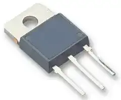


BU323ZG
Bipolar (BJT) Single Transistor, Darlington, NPN, 350 V, 10 A, 150 W, TO-247, Through Hole
- Manufacturer: ONSEMI
- Product type: Single Bipolar Junction Transistors - BJT
- No. of Pins: 3Pins
- Power Dissipation: 150W
- DC Current Gain hFE: 500hFE
- Transistor Mounting: Through Hole
- Transistor Polarity: NPN
- Transition Frequency: 2MHz
- Transistor Case Style: TO-247
- DC Current Gain hFE Min: 500hFE
- Operating Temperature Max: 175°C
- Continuous Collector Current: 10A
- Collector Emitter Voltage Max: 350V
| Delivery and price | |
|---|---|
| Units per pack | 100 |
| Price | 2.29 € |
| Current stock | 10+ |
| Lead time | 30 days |
## BU323Z

## NPN Silicon Power Darlington

## **High Voltage Autoprotected**

The BU323Z is a planar, monolithic, high−voltage power Darlington with a built−in active zener clamping circuit. This device is specifically designed for unclamped, inductive applications such as Electronic Ignition, Switching Regulators and Motor Control, and exhibit the following main features:

## **Features**

- Integrated High−Voltage Active Clamp

## **http://onsemi.com**

## **10 AMPERE DARLINGTON AUTOPROTECTED 360 − 450 VOLTS CLAMP, 150 WATTS**

- Tight Clamping Voltage Window (350 V to 450 V) Guaranteed Over the −40°C to +125°C Temperature Range

- Clamping Energy Capability 100% Tested in a Live Ignition Circuit

360 V CLAMP COLLECTOR 2,4 BASE 1 ~~&~~ EMITTER 3 4 **SOT−93 CASE 340D STYLE 1 TO−247 CASE 340L STYLE 3**

- High DC Current Gain/Low Saturation Voltages Specified Over Full Temperature Range

- Design Guarantees Operation in SOA at All Times

- Offered in Plastic SOT−93/TO−218 Type or TO−220 Packages

• Pb−Free Packages are Available* BASE 1 **MAXIMUM RATINGS Rating Symbol Max Unit** ~~ee ee ee~~ Collector−Emitter Sustaining Voltage VCEO 350 Vdc Collector−Emitter Voltage VEBO 6.0 Vdc 4 Collector Current − Continuous IC 10 Adc − Peak ICM 20 Base Current − Continuous IB 3.0 Adc − Peak IBM 6.0 ~~ee,~~ Total Power Dissipation @ TC = 25 C PD 150 W Derate above 25 C 1.0 W/ C 1 ~~er a~~ Operating and Storage Junction TemperatureRange TJ, Tstg –65 to+175 C 2 3 ~~® ee~~ **THERMAL CHARACTERISTICS Characteristic Symbol Max Unit** ~~ee ee~~ Ss Thermal Resistance, Junction−to−Case R JC 1.0 C/W Maximum Lead Temperature for Soldering TL 260 C ~~——a~~ Purposes: 1/8 ″ from Case for 5 Seconds **NOTE:** ed Stresses exceeding Maximum Ratings may damage the device. Maximum Ratings are stress ratings only. Functional operation above the Recommended Operating Conditions is not implied. Extended exposure to stresses above the Recommended Operating Conditions may affect device reliability.

**NOTE: Effective June 2012 this device will be available only in the TO−247 package. Reference FPCN# 16827.**

## **ORDERING INFORMATION**

- *For additional information on our Pb−Free strategy and soldering details, please download the ON Semiconductor Soldering and Mounting Techniques Reference Manual, SOLDERRM/D.

See detailed ordering and shipping information in the package dimensions section on page 2 of this data sheet.

Publication Order Number: **BU323Z/D**

**1**

© Semiconductor Components Industries, LLC, 2012 **May, 2012 − Rev. 16**

**BU323Z**

## **MARKING DIAGRAMS**

**==> picture [272 x 175] intentionally omitted <==**

**----- Start of picture text -----**<br>
TO−247<br>TO−218<br>BU323Z<br>AYWWG<br>AYWWG<br>BU323Z<br>1 BASE 3 EMITTER<br>1 BASE 3 EMITTER<br>2 COLLECTOR<br>2 COLLECTOR<br>BU323Z = Device Code<br>A = Assembly Location<br>Y = Year<br>WW = Work Week<br>G = Pb−Free Package<br>**----- End of picture text -----**<br>


## **ORDERING INFORMATION**

|**ORDERING INFORMATION**|||
|---|---|---|
|**Device Order Number**|**Package Type**|**Shipping**|
|BU323ZG|TO−218<br>(Pb−Free)|30 Units / Rail|
|BU323ZG|TO−247<br>(Pb−Free)|30 Units / Rail|


**http://onsemi.com**

**2**

**BU323Z**

## **ELECTRICAL CHARACTERISTICS** (TC = 25 � C unless otherwise noted)

|**ELECTRICAL CHARACTERISTICS**(TC= 25�C unless otherwise noted)|**ELECTRICAL CHARACTERISTICS**(TC= 25�C unless otherwise noted)||||||
|---|---|---|---|---|---|---|
|**Characteristic**||**Symbol**|**Min**|**Typ**|**Max**|**Unit**|
|**OFF CHARACTERISTICS (1)**|||||||
|Collector−Emitter Clamping Voltage (IC= 7.0 A)<br>(TC= −40°C to +125°C)||VCLAMP|350|−|450|Vdc|
|Collector−Emitter Cutoff Current<br>(VCE= 200 V, IB= 0)||ICEO|−|−|100|�Adc|
|Emitter−Base Leakage Current<br>(VEB= 6.0 Vdc, IC= 0)||IEBO|−|−|50|mAdc|
|**ON CHARACTERISTICS (1)**|||||||
|Base−Emitter Saturation Voltage<br>(IC= 8.0 Adc, IB= 100 mAdc)<br>(IC= 10 Adc, IB= 0.25 Adc)||VBE(sat)|−<br>−|−<br>−|2.2<br>2.5|Vdc|
|Collector−Emitter Saturation Voltage<br>(IC= 7.0 Adc, IB= 70 mAdc)<br>(TC= 125°C)<br>(IC= 8.0 Adc, IB= 0.1 Adc)<br>(TC= 125°C)<br>(IC= 10 Adc, IB= 0.25 Adc)||VCE(sat)|−<br>−<br>−<br>−<br>−|−<br>−<br>−<br>−<br>−|1.6<br>1.8<br>1.8<br>2.1<br>1.7|Vdc|
|Base−Emitter On Voltage<br>(IC= 5.0 Adc, VCE= 2.0 Vdc)<br>(TC= −40°C to +125°C)<br>(IC= 8.0 Adc, VCE= 2.0 Vdc)||VBE(on)|1.1<br>1.3|−<br>−|2.1<br>2.3|Vdc|
|Diode Forward Voltage Drop<br>(IF= 10 Adc)||VF|−|−|2.5|Vdc|
|DC Current Gain<br>(IC= 6.5 Adc, VCE= 1.5 Vdc)<br>(TC= −40°C to +125°C)<br>(IC= 5.0 Adc, VCE= 4.6 Vdc)||hFE|150<br>500|−<br>−|−<br>3400|−|
|**DYNAMIC CHARACTERISTICS**|||||||
|Current Gain Bandwidth<br>(IC= 0.2 Adc, VCE= 10 Vdc, f = 1.0 MHz)||fT|−|−|2.0|MHz|
|Output Capacitance<br>(VCB= 10 Vdc, IE= 0, f = 1.0 MHz)||Cob|−|−|200|pF|
|Input Capacitance<br>(VEB= 6.0 V)||Cib|−|−|550|pF|
|**CLAMPING ENERGY (see notes)**|||||||
|Repetitive Non−Destructive Energy Dissipated at turn−off:<br>(IC= 7.0 A, L = 8.0 mH, RBE= 100�) (see Figures 2 and 4)||WCLAMP|200|−|−|mJ|
|**SWITCHING CHARACTERISTICS: Inductive Load**(L = 10 mH)|||||||
|Fall Time|(IC= 6.5 A, IB1= 45 mA,<br>VBE(off)= 0, RBE(off)= 0,<br>VCC= 14 V, VZ= 300 V)|tfi|−|625|−|ns|
|Storage Time||tsi|−|10|30|�s|
|Cross−over Time||tc|−|1.7|−|�s|


1. Pulse Test: Pulse Width ≤ 300 � s, Duty Cycle = 2.0%.

**http://onsemi.com**

**3**

**BU323Z**

**==> picture [214 x 136] intentionally omitted <==**

**----- Start of picture text -----**<br>
IC<br>INOM = 6.5 A<br>Output transistor turns on: IC = 40 mA<br>High Voltage Circuit turns on: IC = 20 mA<br>Avalanche diode turns on: IC = 100 �A<br>250 V 300 V 340 V VCLAMPV NOMINALCE<br>Icer Leakage Current = 400 V<br>**----- End of picture text -----**<br>


**==> picture [218 x 125] intentionally omitted <==**

**----- Start of picture text -----**<br>
L INDUCTANCE<br>MERCURY CONTACTS (8 mH)<br>WETTED RELAY<br>IC CURRENT<br>VCE SOURCE<br>MONITOR<br>(VGATE)<br>RBE = 100 � 0.1 �<br>IB CURRENTSOURCE IVB2BEoff SOURCE MONITORIC NONINDUCTIVE<br>**----- End of picture text -----**<br>


**Figure 1. IC = f(VCE) Curve Shape**

**Figure 2. Basic Energy Test Circuit**

By design, the BU323Z has a built−in avalanche diode and a special high voltage driving circuit. During an auto−protect cycle, the transistor is turned on again as soon as a voltage, determined by the zener threshold and the network, is reached. This prevents the transistor from going into a Reverse Bias Operating limit condition. Therefore, the device will have an extended safe operating area and will always appear to be in “FBSOA.” Because of the built−in zener and associated network, the IC = f(VCE) curve exhibits an unfamiliar shape compared to standard products as shown in Figure 1.

The bias parameters, VCLAMP, IB1, VBE(off), IB2, IC, and the inductance, are applied according to the Device Under Test (DUT) specifications. VCE and IC are monitored by the test system while making sure the load line remains within the limits as described in Figure 4.

Note: All BU323Z ignition devices are 100% energy tested, per the test circuit and criteria described in Figures 2 and 4, to the minimum guaranteed repetitive energy, as specified in the device parameter section. The device can sustain this energy on a repetitive basis without degrading any of the specified electrical characteristics of the devices. The units under test are kept functional during the complete test sequence for the test conditions described: IC(peak) = 7.0 A, ICH = 5.0 A, ICL = 100 mA, IB = 100 mA, RBE = 100 �, Vgate = 280 V, L = 8.0 mH

**==> picture [243 x 169] intentionally omitted <==**

**----- Start of picture text -----**<br>
10<br>300 �s<br>TC = 25°C 1�ms<br>1<br>10�ms<br>250�ms<br>0.1<br>THERMAL LIMIT<br>0.01<br>SECOND BREAKDOWN LIMIT<br>CURVES APPLY BELOW<br>RATED VCEO<br>0.001<br>10 100 340�V 1000<br>VCE, COLLECTOR-EMITTER VOLTAGE (VOLTS)<br>IC, COLLECTOR CURRENT (AMPS)<br>**----- End of picture text -----**<br>


**Figure 3. Forward Bias Safe Operating Area**

**http://onsemi.com 4**

**BU323Z**

**==> picture [203 x 637] intentionally omitted <==**

**----- Start of picture text -----**<br>
IC<br>ICPEAK<br>IC HIGH<br>IC LOW<br>VCE<br>(a) VGATE MIN<br>IC<br>ICPEAK<br>IC HIGH<br>IC LOW<br>VCE<br>(b) VGATE MIN<br>IC<br>ICPEAK<br>IC HIGH<br>IC LOW<br>VCE<br>(c) VGATE MIN<br>IC<br>ICPEAK<br>IC HIGH<br>IC LOW<br>VCE<br>(d) VGATE MIN<br>**----- End of picture text -----**<br>


The shaded area represents the amount of energy the device can sustain, under given DC biases (IC/IB/VBE(off)/ RBE), without an external clamp; see the test schematic diagram, Figure 2.

The transistor PASSES the Energy test if, for the inductive load and ICPEAK/IB/VBE(off) biases, the VCE remains outside the shaded area and greater than the VGATE minimum limit, Figure 4a.

The transistor FAILS if the VCE is less than the VGATE (minimum limit) at any point along the VCE/IC curve as shown on Figures 4b, and 4c. This assures that hot spots and uncontrolled avalanche are not being generated in the die, and the transistor is not damaged, thus enabling the sustained energy level required.

The transistor FAILS if its Collector/Emitter breakdown voltage is less than the VGATE value, Figure 4d.

**Figure 4. Energy Test Criteria for BU323Z**

**http://onsemi.com**

**5**

**BU323Z**

**==> picture [491 x 615] intentionally omitted <==**

**----- Start of picture text -----**<br>
10000 10000<br>TYPICAL<br>TJ = 125°C<br>1000 1000<br>-40°C TYP - 6Σ<br>TYP + 6Σ<br>100 25°C 100<br>VCE = 5 V, TJ = 25°C<br>VCE = 1.5 V<br>10 10<br>100 1000 10000 100 1000 10000 100000<br>IC, COLLECTOR CURRENT (MILLIAMPS) IC, COLLECTOR CURRENT (MILLIAMPS)<br>Figure 5. DC Current Gain Figure 6. DC Current Gain<br>5.0<br>4.5 IC = 3 A TJ = 25°C 2.22.4 IC/IB = 150<br>4.0 2.0 TJ = 125°C<br>3.5<br>1.8<br>3.0 5 A 8 A 1.6<br>2.5 10 A<br>1.4<br>2.0 7 A 1.2<br>1.5 1.0<br>1.0 0.8 25°C<br>0.5 0.6<br>0 0.4<br>1 10 100 0.1 1 10<br>IB, BASE CURRENT (MILLIAMPS) IC, COLLECTOR CURRENT (AMPS)<br>Figure 7. Collector Saturation Region Figure 8. Collector−Emitter Saturation Voltage<br>2.0 2.0<br>IC/IB = 150 VCE = 2 VOLTS<br>1.8<br>1.8<br>1.6<br>1.6 TJ = 25°C<br>1.4 TJ = 25°C<br>1.4<br>1.2<br>1.2 125°C 1.0 125°C<br>1.0 0.8<br>0.8 0.6<br>0.1 1 10 0.1 1 10<br>IC, COLLECTOR CURRENT (AMPS) IC, COLLECTOR CURRENT (AMPS)<br>hFE, DC CURRENT GAIN hFE, DC CURRENT GAIN<br>VCE, COLLECTOR-EMITTER VOLTAGE (VOLTS) VCE, COLLECTOR-EMITTER VOLTAGE (VOLTS)<br>VBE, BASE-EMITTER VOLTAGE (VOLTS)<br>VBE(on), BASE-EMITTER VOLTAGE (VOLTS)<br>**----- End of picture text -----**<br>


**Figure 9. Base−Emitter Saturation Voltage**

**Figure 10. Base−Emitter “ON” Voltages**

**http://onsemi.com**

**6**

**BU323Z**

## **PACKAGE DIMENSIONS**

**SOT−93 (TO−218)** CASE 340D−02 ISSUE E

**==> picture [204 x 179] intentionally omitted <==**

**----- Start of picture text -----**<br>
C<br>B Q E<br>U 4<br>A<br>S L<br>K 1 2 3<br>J<br>D<br>H<br>V<br>G<br>**----- End of picture text -----**<br>


**==> picture [124 x 188] intentionally omitted <==**

**----- Start of picture text -----**<br>
NOTES:<br>1. DIMENSIONING AND TOLERANCING PER ANSI<br>Y14.5M, 1982.<br>2. CONTROLLING DIMENSION: MILLIMETER.<br>MILLIMETERS INCHES<br>DIM MIN MAX MIN MAX<br>A --- 20.35 --- 0.801<br>B 14.70 15.20 0.579 0.598<br>C 4.70 4.90 0.185 0.193<br>D 1.10 1.30 0.043 0.051<br>E 1.17 1.37 0.046 0.054<br>G 5.40 5.55 0.213 0.219<br>H 2.00 3.00 0.079 0.118<br>J 0.50 0.78 0.020 0.031<br>K 31.00 REF 1.220 REF<br>L --- 16.20 --- 0.638<br>Q 4.00 4.10 0.158 0.161<br>S 17.80 18.20 0.701 0.717<br>U 4.00 REF 0.157 REF<br>V 1.75 REF 0.069<br>STYLE 1:<br>PIN 1. BASE<br>2. COLLECTOR<br>3. EMITTER<br>4. COLLECTOR<br>**----- End of picture text -----**<br>


**TO−247** CASE 340L−02 ISSUE F

**==> picture [312 x 213] intentionally omitted <==**

**----- Start of picture text -----**<br>
−T−<br>C<br>− B−<br>E<br>U L<br>N<br>4<br>A<br>−Q−<br>1 2 3 0.63 (0.025) [M] T B M<br>P<br>−Y−<br>K<br>W J<br>F 2 PL H<br>G<br>D 3 PL<br>0.25 (0.010) [M] Y Q S<br>**----- End of picture text -----**<br>


NOTES:

1. DIMENSIONING AND TOLERANCING PER ANSI Y14.5M, 1982.

2. CONTROLLING DIMENSION: MILLIMETER.

|S|**DIM**|**MILLIMETERS**|**MILLIMETERS**|**INCHES**|**INCHES**|
|---|---|---|---|---|---|
|||**MIN**|**MAX**|**MIN**|**MAX**|
||**A**<br>|20.32|21.08|0.800|8.30|
||**B**|15.75|16.26|0.620|0.640|
||**C**|4.70|5.30|0.185|0.209|
||**D**|1.00|1.40|0.040|0.055|
||**E**|190|260|0075|0102|
||**F**<br>|.<br>1.65<br>|.<br>2.13<br>|.<br>0.065<br>|.<br>0.084<br>|
||**G**|5.45 BSC||0.215 BSC||
||**H**|1.50|2.49|0.059|0.098|
||**J**|0.40|0.80|0.016|0.031|
||**K**|19.81|20.83|0.780|0.820|
||**L**|5.40|6.20|0.212|0.244|
||**N**|4.32|5.49|0.170|0.216|
||**P**|---|4.50|---|0.177|
||**Q**|3.55|3.65|0.140|0.144|
||**U**|6.15 BSC||0.242 BSC||
||**W**|2.87|3.12|0.113|0.123|
||TYLE 3:<br>PIN 1. BASE<br>2. COLLECTOR<br>3. EMITTER<br>4COLLECTOR|||||


**http://onsemi.com**

**7**

**BU323Z**

**ON Semiconductor** and          are registered trademarks of Semiconductor Components Industries, LLC (SCILLC).  SCILLC reserves the right to make changes without further notice to any products herein.  SCILLC makes no warranty, representation or guarantee regarding the suitability of its products for any particular purpose, nor does SCILLC assume any liability arising out of the application or use of any product or circuit, and specifically disclaims any and all liability, including without limitation special, consequential or incidental damages. “Typical” parameters which may be provided in SCILLC data sheets and/or specifications can and do vary in different applications and actual performance may vary over time.  All operating parameters, including “Typicals” must be validated for each customer application by customer’s technical experts.  SCILLC does not convey any license under its patent rights nor the rights of others.  SCILLC products are not designed, intended, or authorized for use as components in systems intended for surgical implant into the body, or other applications intended to support or sustain life, or for any other application in which the failure of the SCILLC product could create a situation where personal injury or death may occur.  Should Buyer purchase or use SCILLC products for any such unintended or unauthorized application, Buyer shall indemnify and hold SCILLC and its officers, employees, subsidiaries, affiliates, and distributors harmless against all claims, costs, damages, and expenses, and reasonable attorney fees arising out of, directly or indirectly, any claim of personal injury or death associated with such unintended or unauthorized use, even if such claim alleges that SCILLC was negligent regarding the design or manufacture of the part.  SCILLC is an Equal Opportunity/Affirmative Action Employer.  This literature is subject to all applicable copyright laws and is not for resale in any manner.

## **PUBLICATION ORDERING INFORMATION**

**N. American Technical Support** : 800−282−9855 Toll Free USA/Canada

## **LITERATURE FULFILLMENT** :

Literature Distribution Center for ON Semiconductor USA/Canada P.O. Box 5163, Denver, Colorado 80217 USA **Europe, Middle East and Africa Technical Support: Phone** : 303−675−2175 or 800−344−3860 Toll Free USA/Canada Phone: 421 33 790 2910 **Fax** : 303−675−2176 or 800−344−3867 Toll Free USA/Canada **Japan Customer Focus Center Email** : orderlit@onsemi.com Phone: 81−3−5817−1050

**ON Semiconductor Website** : **www.onsemi.com**

**Order Literature** : http://www.onsemi.com/orderlit For additional information, please contact your local Sales Representative

**BU323Z/D**

**http://onsemi.com**

**8**
Updated at February 9, 2023
onsemi is a premier global supplier of intelligent power and sensing technologies, driving disruptive innovations across the automotive, industrial, and cloud infrastructure markets. Recognized for their commitment to sustainability and reliable supply chains, the company accelerates advancements in vehicle electrification, industrial automation, and 5G networks by solving the industry's most complex design challenges. At the core of their portfolio is an industry-leading selection of discrete semiconductors. This extensive range features thousands of high-performance bipolar transistors, single and dual MOSFETs, and a comprehensive array of diodes, including Zener, Schottky, and fast-recovery rectifiers. Engineered for superior thermal performance and energy efficiency, these foundational components are critical for demanding power conversion, switching, and signal conditioning applications. Beyond essential discretes, onsemi provides a robust suite of advanced power management and circuit protection solutions. Their lineup includes intelligent power modules, single IGBTs, and transient voltage suppression (TVS) diodes designed to safeguard sensitive circuitry. Complimented by integrated passive filters, AC/DC LED driver ICs, and specialized sub-2.4GHz RF transceivers, onsemi equips engineers with the scalable, high-quality technologies needed to build a cleaner, smarter, and more connected world.
About Novapart
Novapart is a B2B electronic component broker specialising in stock shortages and cost reduction. We source hard-to-find parts and identify compliant alternatives across a catalogue of 410,000+ components from 500+ manufacturers.
Learn more →Stock Shortage Specialist
When a component is unavailable, discontinued or has an unacceptable lead time, we tap into our network of vetted European and Asian distributors to source what you need — without compromising on quality or traceability.
Request a quote →Compliant Alternatives
We identify pin-to-pin, electrically equivalent substitutes that meet the same certifications (RoHS, AEC-Q100, REACH) as your original specification — validated against datasheets, not just part numbers. Often at a lower cost.
BOM Analysis service →