


BTW69-1200N
Thyristor, 1.2 kV, 50 mA, 31 A, 50 A, TOP-3, 3 Pins
- Manufacturer: STMICROELECTRONICS
- Product type: Thyristors - SCRs
- Peak Repetitive Off-State Voltage, Vdrm:1.2kV; Gate Trigger Current Max, Igt:50mA; Current It av:31A; On State RMS Current IT(rms):50A; Thyristor Case Style:TOP-3; No. of Pins:3Pins; Pea
- MSL: -
- SVHC: No SVHC (25-Jun-2025)
- No. of Pins: 3Pins
- Product Range: BTW69
- Thyristor Mounting: Through Hole
- Holding Current Max: 100mA
- On State RMS Current: 50A
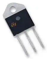
- Thyristor Case Style: TOP-3
- Average On State Current: 31A
- Gate Trigger Current Max: 50mA
- Gate Trigger Voltage Max: 1.3V
- Operating Temperature Max: 125°C
- Peak Non Repetitive Surge Current: 700A
- Peak Repetitive Off State Voltage: 1.2kV
| Delivery and price | |
|---|---|
| Units per pack | 250 |
| Price | 3.51 € |
| Current stock | 500+ |
| Lead time | 30 days |
## **BTW69-1200N** ## 50 A – 1200 V non insulated SCR thyristor **Datasheet** - **production data** ## **Features** **==> picture [72 x 162] intentionally omitted <==** **----- Start of picture text -----**<br> A<br>G<br>K<br>A<br>K<br>A<br>G<br>**----- End of picture text -----**<br> **TOP3 non insulated** ## **Description** Available in non insulated TOP3 high power package, the BTW69-1200N is suitable for applications where power switching and power dissipation are critical, such as by-pass switch, controlled AC rectifier bridge, in solid state relay, battery charger, uninterruptible power supply, welding equipment and motor driver applications. Based on a clip assembly technology, the BTW69-1200N offers a superior performance in surge current handling and thermal cooling capabilities. **Table 1. Device summary** |**Symbol**|**Value**| |---|---| |IT(RMS)|50 A| |VDRM/VRRM|1200 V| |IGT|50 mA| - On-state rms current: 50 A - Blocking voltage: 1200 V - Gate current: 50 mA ## **Applications** - Solid state relay - Battery charging system - Uninterruptible power supply - Variable speed motor drive - Industrial welding systems - By pass AC switch June 2013 DocID024685 Rev 1 1/9 This is information on a product in full production. _www.st.com_ **Characteristics** **BTW69-1200N** ## **1 Characteristics** **Table 2. Absolute maximum ratings (limiting values)** |**Symbol**|**Parameter**|**Parameter**|**Parameter**|**Value**|**Unit**| |---|---|---|---|---|---| |IT(RMS)|On-state current rms (180° conduction angle)||Tc= 102 °C|50|A| |IT(AV)|Average on-state current (180° conduction angle)||Tc= 102 °C|31|A| |ITSM|Non repetitive surge peak on-state<br>current|tp= 8.3 ms|Tj= 25 °C|763|A| |||tp= 10 ms||700|| |I²t|I²t Value|tp= 10 ms|Tj= 25 °C|2450|A2S| |dI/dt|Critical rate of rise of on-state current<br>Gate supply: IG= 100 mA, dIG/dt = 1 A/µs|||100|A/µs| |IGM|Peak gate current|tp= 20 µs|Tj= 125 °C|8|A| |PG(AV)|Average gate power dissipation||Tj= 125 °C|1|W| |Tstg<br>Tj|Storage junction temperature range<br>Operating junction temperature range|||- 40 to + 150<br>- 40 to + 125|°C| |VGM|Maximum peak reverse gate voltage|||5|V| **Table 3. Electrical characteristics (Tj = 25 °C, unless otherwise specified)** ||||||| |---|---|---|---|---|---| |**Symbol**|**Test conditions**|||**Value**|**Unit**| |IGT|VD= 12 V, RL= 33||MIN.|8|mA| ||||MAX.|50|| |VGT|||MAX.|1.3|V| |VGD|VD= VDRM,RL= 3.3 k|Tj= 125 °C|MIN.|0.2|V| |IH|IT= 500 mA, gate open||MAX.|100|mA| |IL|IG= 1.2 x IGT||TYP.|125|mA| |tgt|IT= 50 A, VD= VDRM, IG= 200 mA, dIG/dt|= 0.2 A/µs|TYP.|2|µs| |dV/dt|VD= 67% VDRM,gate open|Tj= 125 °C|MIN.|1000|V/µs| |tq|VD= 800 V, ITM= 50 A, VR= 75 V,<br>tp= 100 µs, dITM/dt = 30 A/µs,<br>dVD/dt = 20 V/µs|Tj= 125 °C|TYP.|100|µs| |VTM|ITM= 100 A, tp= 380 µs|Tj= 25 °C|MAX.|1.6|V| |Vt0|Threshold voltage|Tj= 125 °C|MAX.|0.9|V| |RD|Dynamic resistance|Tj= 125 °C|MAX.|8.5|m| |IDRM<br>IRRM|VD= VDRM<br>VR= VRRM|Tj= 25 °C|MAX.|10|µA| |||Tj= 125 °C||5|mA| 2/9 DocID024685 Rev 1 **Characteristics** **BTW69-1200N** **Table 4. Thermal resistance** ||**Table 4. Thermal resistance**||| |---|---|---|---| |**Symbol**|**Parameter**|**Value**|**Unit**| |Rth(j-c)<br>Junction to|case (DC, typ.)|0.45|°C/W| |Rth(j-a)<br>Junction to|ambient (DC)|50|°C/W| **Figure 1. Maximum average power dissipation versus average on-state current** **Figure 2. Correlation between maximum average power dissipation and maximum allowable temperatures** **==> picture [462 x 356] intentionally omitted <==** **----- Start of picture text -----**<br> 55 P(W) P(AV)(W) Tc(°C) 100.2<br>50 � = 120° � = 180° DC 50 � = 180° 102.7<br>45 � = 90° 105.2<br>40 � = 60° 40 107.7<br>35 � = 30° 110.2<br>30 30<br>25 (assembly) RTH 112.7<br>20 20 0 °C/W 115.2<br>15 360° 1 °C/W2 °C/W 117.7<br>10 10 3 °C/W 120.2<br>5 IT(AV)(A) � T a (°C) 122.7<br>0 0<br>0 5 10 15 20 25 30 35 40 0 25 50 75 100 125<br>Figure 3. Average and DC on-state current Figure 4. Average and DC on-state current<br>versus case temperature versus ambient temperature<br>55 IT(AV)(A) 3.0 IT(AV)(A)<br>DC<br>50 DC<br>45 � = 120° 2.5<br>40 � = 60° � = 90° � = 180°<br>35 � = 180° 2.0<br>30<br>1.5<br>25<br>20<br>1.0<br>15<br>10 � = 30° 0.5<br>5 T case (°C) Ta(°C)<br>0 0.0<br>0 25 50 75 100 125 0 25 50 75 100 125<br>**----- End of picture text -----**<br> DocID024685 Rev 1 3/9 **Characteristics** **BTW69-1200N** **Figure 5. Relative variation of thermal impedance versus pulse duration** **Figure 6. Relative variation of gate trigger current and gate trigger voltage versus junction temperature (typical value)** **==> picture [462 x 160] intentionally omitted <==** **----- Start of picture text -----**<br> 1.0E+00 K=[Zth/Rth] 1.8 IGT,VGT [T j] / IGT,VGT [T =25°Cj ]<br>Z th(j-c) Z th(j-a) 1.5 IGT<br>1.3<br>1.0 V GT<br>1.0E-01<br>0.8<br>0.5<br>0.3<br>1.0E-02 tp(s) T (°C)j<br>0.0<br>1.0E-03 1.0E-02 1.0E-01 1.0E+00 1.0E+01 1.0E+02 1.0E+03<br>-40 -20 0 20 40 60 80 100 125<br>**----- End of picture text -----**<br> **Figure 7. Relative variation of holding, and latching currents versus junction temperature (typical values)** **Figure 8. Surge peak on-state current versus number of cycles** **==> picture [462 x 160] intentionally omitted <==** **----- Start of picture text -----**<br> IH,IL [T j] / IH,IL [T =25°Cj ]<br>1.8 ITSM(A)<br>600<br>1.5 550<br>IL 500 tp=10ms<br>1.3 IH 450400 Non repetitive One cycle<br>1.0 350 Tj initial=25 °C<br>300<br>0.8 250<br>200<br>0.5 150<br>100<br>0.3 T (°C)j 500 T RepetitiveC =102°C Number of cycles<br>0.0<br>1 10 100 1000<br>-40 -20 0 20 40 60 80 100 125<br>**----- End of picture text -----**<br> **Figure 9. Non repetitive surge peak on-state current and corresponding value of I[2] t versus sinusoidal pulse** **==> picture [215 x 140] intentionally omitted <==** **----- Start of picture text -----**<br> ITSM(A), I t 2 (A s2 )<br>10000<br>dI/dt limitation: 100 A/µs Tj initial=25 °C<br>I²t<br>ITSM<br>1000<br>100<br>pulse with width tp < 10 ms tp(ms)<br>10<br>0.01 0.10 1.00 10.00<br>**----- End of picture text -----**<br> **Figure 10. On-state characteristics (maximum values)** **==> picture [215 x 144] intentionally omitted <==** **----- Start of picture text -----**<br> ITM (A)<br>1000<br>100<br>10<br>Tj max :<br>Tj =125 °C Tj =25 °C VTM (V) RVd to = 8.5 m= 0.9 V�<br>1<br>0.0 1.0 2.0 3.0 4.0<br>**----- End of picture text -----**<br> 4/9 DocID024685 Rev 1 **Characteristics** **BTW69-1200N** **Figure 11. Relative variation of leakage current versus junction temperature for different values of blocking voltage (600 and 800 V)** **Figure 12. Relative variation of leakage current versus junction temperature for different values of blocking voltage (1000 and 1200 V)** **==> picture [462 x 160] intentionally omitted <==** **----- Start of picture text -----**<br> IDRM,IRRM [Tj;V DRM,VRRM] / IDRM,IRRM IDRM,IRRM [Tj;V DRM,VRRM] / IDRM,IRRM<br>1.0E+00 1.0E+00<br>1.0E-01 VDRM=VRRM=800 V 1.0E-01 VDRM=VRRM=1200 V<br>1.0E-02 VDRM=VRRM=600 V 1.0E-02 VDRM=VRRM=1000 V<br>1.0E-03 1.0E-03<br>Tj(°C) T j (°C)<br>1.0E-04 1.0E-04<br>25 50 75 100 125 25 50 75 100 125<br>**----- End of picture text -----**<br> DocID024685 Rev 1 5/9 **Package information** **BTW69-1200N** ## **2 Package information** - Epoxy meets UL94,V0 - Lead-free packages - Cooling method: by conduction (C) - Recommended torque value: 0.9 to 1.2 N·m In order to meet environmental requirements, ST offers these devices in different grades of ECOPACK[®] packages, depending on their level of environmental compliance. ECOPACK[®] specifications, grade definitions and product status are available at: _www.st.com._ ECOPACK[®] is an ST trademark. ## **Figure 13. TOP3 dimension definitions** **==> picture [198 x 199] intentionally omitted <==** **----- Start of picture text -----**<br> H A<br>R B<br>ØL<br>K<br>F G<br>P<br>C<br>D<br>J J<br>E<br>**----- End of picture text -----**<br> 6/9 DocID024685 Rev 1 **BTW69-1200N** **Package information** ## **Table 5. TOP3 dimension values** ||**Table 5. TOP3 dimension values**|**Table 5. TOP3 dimension values**|**Table 5. TOP3 dimension values**|**Table 5. TOP3 dimension values**| |---|---|---|---|---| |**Ref.**|**Dimensions**|||| ||**Millimeters**||**Inches**|| ||**Min.**|**Max.**|**Min.**|**Max.**| |A|4.4|4.6|0.173|0.181| |B|1.45|1.55|0.057|0.061| |C|14.35|15.60|0.565|0.614| |D|0.5|0.7|0.020|0.028| |E|2.7|2.9|0.106|0.114| |F|15.8|16.5|0.622|0.650| |G|20.4|21.1|0.815|0.831| |H|15.1|15.5|0.594|0.610| |J|5.4|5.65|0.213|0.222| |K|3.4|3.65|0.134|0.144| |ØL|4.08|4.17|0.161|0.164| |P|1.20|1.40|0.047|0.055| |R|4.60 typ.||0.181 typ.|| DocID024685 Rev 1 7/9 **Ordering information** **BTW69-1200N** ## **3 Ordering information** ## **Figure 14. Ordering information scheme** **==> picture [192 x 103] intentionally omitted <==** **----- Start of picture text -----**<br> BTW 69 - 1200 N<br>Standard SCR series<br>Type<br>69 = 50 A<br>Voltage<br>1200 = 1200 V<br>Package<br>N = TOP3 non insulated<br>**----- End of picture text -----**<br> **==> picture [140 x 10] intentionally omitted <==** **----- Start of picture text -----**<br> Table 6. Ordering information<br>**----- End of picture text -----**<br> |**Order code**|**Marking**|**Package**|**Weight**|**Base qty**|**Delivery mode**| |---|---|---|---|---|---| |BTW69-1200N|BTW691200N|TOP3|4.55 g|30|Tube| ## **4 Revision history** **Table 7. Document revision history** |**Date**|**Revision**|**Changes**| |---|---|---| |14-Jun-2013|1|Initial release.| 8/9 DocID024685 Rev 1 **BTW69-1200N** ## **Please Read Carefully:** Information in this document is provided solely in connection with ST products. STMicroelectronics NV and its subsidiaries (“ST”) reserve the right to make changes, corrections, modifications or improvements, to this document, and the products and services described herein at any time, without notice. All ST products are sold pursuant to ST’s terms and conditions of sale. Purchasers are solely responsible for the choice, selection and use of the ST products and services described herein, and ST assumes no liability whatsoever relating to the choice, selection or use of the ST products and services described herein. No license, express or implied, by estoppel or otherwise, to any intellectual property rights is granted under this document. If any part of this document refers to any third party products or services it shall not be deemed a license grant by ST for the use of such third party products or services, or any intellectual property contained therein or considered as a warranty covering the use in any manner whatsoever of such third party products or services or any intellectual property contained therein. **UNLESS OTHERWISE SET FORTH IN ST’S TERMS AND CONDITIONS OF SALE ST DISCLAIMS ANY EXPRESS OR IMPLIED WARRANTY WITH RESPECT TO THE USE AND/OR SALE OF ST PRODUCTS INCLUDING WITHOUT LIMITATION IMPLIED WARRANTIES OF MERCHANTABILITY, FITNESS FOR A PARTICULAR PURPOSE (AND THEIR EQUIVALENTS UNDER THE LAWS OF ANY JURISDICTION), OR INFRINGEMENT OF ANY PATENT, COPYRIGHT OR OTHER INTELLECTUAL PROPERTY RIGHT.** **ST PRODUCTS ARE NOT AUTHORIZED FOR USE IN WEAPONS. NOR ARE ST PRODUCTS DESIGNED OR AUTHORIZED FOR USE IN: (A) SAFETY CRITICAL APPLICATIONS SUCH AS LIFE SUPPORTING, ACTIVE IMPLANTED DEVICES OR SYSTEMS WITH PRODUCT FUNCTIONAL SAFETY REQUIREMENTS; (B) AERONAUTIC APPLICATIONS; (C) AUTOMOTIVE APPLICATIONS OR ENVIRONMENTS, AND/OR (D) AEROSPACE APPLICATIONS OR ENVIRONMENTS. WHERE ST PRODUCTS ARE NOT DESIGNED FOR SUCH USE, THE PURCHASER SHALL USE PRODUCTS AT PURCHASER’S SOLE RISK, EVEN IF ST HAS BEEN INFORMED IN WRITING OF SUCH USAGE, UNLESS A PRODUCT IS EXPRESSLY DESIGNATED BY ST AS BEING INTENDED FOR “AUTOMOTIVE, AUTOMOTIVE SAFETY OR MEDICAL” INDUSTRY DOMAINS ACCORDING TO ST PRODUCT DESIGN SPECIFICATIONS. PRODUCTS FORMALLY ESCC, QML OR JAN QUALIFIED ARE DEEMED SUITABLE FOR USE IN AEROSPACE BY THE CORRESPONDING GOVERNMENTAL AGENCY.** Resale of ST products with provisions different from the statements and/or technical features set forth in this document shall immediately void any warranty granted by ST for the ST product or service described herein and shall not create or extend in any manner whatsoever, any liability of ST. ST and the ST logo are trademarks or registered trademarks of ST in various countries. Information in this document supersedes and replaces all information previously supplied. The ST logo is a registered trademark of STMicroelectronics. All other names are the property of their respective owners. © 2013 STMicroelectronics - All rights reserved STMicroelectronics group of companies Australia - Belgium - Brazil - Canada - China - Czech Republic - Finland - France - Germany - Hong Kong - India - Israel - Italy - Japan - Malaysia - Malta - Morocco - Philippines - Singapore - Spain - Sweden - Switzerland - United Kingdom - United States of America **www.st.com** DocID024685 Rev 1 9/9
Updated at April 28, 2026
STMicroelectronics is a global leader in the semiconductor industry, recognized for developing highly integrated, energy-efficient solutions that power modern electronics. With a strong focus on innovation, ST provides a comprehensive portfolio of microelectronics that address the demanding requirements of industrial, automotive, communications, and consumer applications. Our extensive selection of STMicroelectronics components is built around a robust lineup of discrete semiconductors and circuit protection devices. We offer a wide variety of single MOSFETs, Schottky diodes, and fast and ultrafast recovery rectifier diodes, designed to deliver exceptional efficiency and thermal performance in power management and conversion systems. For robust circuit protection, our inventory features hundreds of transient voltage suppressors and TVS diodes that safeguard sensitive electronic components against destructive voltage spikes. In addition to core power discretes like TRIACs, SCRs, bipolar transistors, and single IGBTs, our STMicroelectronics range includes specialized integrated passive filters and MEMS sensors. Furthermore, ST offers advanced integrated passive devices, such as baluns and RF filters, which utilize high-quality monolithic RF IPD processes on glass or high-resistance silicon substrates. These components provide competitive cost structures, reduced power losses, and simplified RFIC-to-antenna matching, ensuring optimal system performance and delivering the reliability required for next-generation wireless and power designs.
About Novapart
Novapart is a B2B electronic component broker specialising in stock shortages and cost reduction. We source hard-to-find parts and identify compliant alternatives across a catalogue of 410,000+ components from 500+ manufacturers.
Learn more →Stock Shortage Specialist
When a component is unavailable, discontinued or has an unacceptable lead time, we tap into our network of vetted European and Asian distributors to source what you need — without compromising on quality or traceability.
Request a quote →Compliant Alternatives
We identify pin-to-pin, electrically equivalent substitutes that meet the same certifications (RoHS, AEC-Q100, REACH) as your original specification — validated against datasheets, not just part numbers. Often at a lower cost.
BOM Analysis service →