


BTW67-600
Thyristor Module, 32 A, 600 V
- Manufacturer: STMICROELECTRONICS
- Product type: Thyristors - SCR Modules
- No. of Pins: 3Pins
- SCR Module Type: Single SCR
- Thyristor Mounting: Panel
- Holding Current Max: 150mA
- On State RMS Current: 50A
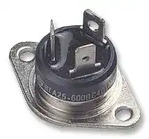
- Thyristor Case Style: RD-91
- Average Forward Current: 32A
- Average On State Current: 32A
- Gate Trigger Current Max: 80mA
- Gate Trigger Voltage Max: 1.3V
- Operating Temperature Max: 125°C
- Repetitive Peak Reverse Voltage: 600V
- Peak Non Repetitive Surge Current: 610A
- Peak Repetitive Off State Voltage: 600V
| Delivery and price | |
|---|---|
| Units per pack | 5 |
| Price | 6.47 € |
| Current stock | 10+ |
| Lead time | 30 days |
**==> picture [61 x 38] intentionally omitted <==**

**----- Start of picture text -----**<br>
®<br>**----- End of picture text -----**<br>


## ® **BTW67 and BTW69 Series**

## **STANDARD**

## 50A SCRS

**Table 1: Main Features**

|**Symbol**|**Value**|**Unit**|
|---|---|---|
|**IT(RMS)**|50|A|
|**VDRM/VRRM**|600 to 1200|V|
|**IGT**|80|mA|


## **DESCRIPTION**

Available in high power packages, the **BTW67 / BTW69** Series is suitable in applications where power handling and power dissipation are critical, such as solid state relays, welding equipment, high power motor control.

Based on a clip assembly technology, they offer a superior performance in surge current handling capabilities.

Thanks to their internal ceramic pad, they provide high voltage insulation (2500VRMS), complying with UL standards (file ref: E81734).

**==> picture [218 x 175] intentionally omitted <==**

**----- Start of picture text -----**<br>
A<br>G<br>K<br>K<br>G A<br>K<br>A<br>G<br>RD91 TOP3 Ins.<br>(BTW67) (BTW69)<br>**----- End of picture text -----**<br>


**Table 2: Order Codes**

|**Table 2: Order Codes**||
|---|---|
|**Part Numbers**|**Marking**|
|BTW67-xxx|BTW67xxx|
|BTW69-xxxRG|BTW69xxx|


**Table 3: Absolute Ratings** (limiting values)

|**Symbol**|**Parameter**|||**Value**|**Unit**|
|---|---|---|---|---|---|
|IT(RMS)|RMS on-state current<br>(180° conduction angle)|RD91<br>TOP3 Ins.|Tc= 70°C|50|A|
||||Tc= 75°C|||
|IT(AV)|Average on-state current<br>(180° conduction angle)|RD91<br>TOP3 Ins.|Tc= 70°C|32|A|
||||Tc= 75°C|||
|ITSM|Non repetitive surge peak on-state current|tp= 8.3 ms<br>tp= 10 ms|Tj= 25°C|610|A|
|||||580||
|I²t|I²t Value for fusing||Tj= 25°C|1680|A2S|
|dI/dt|Critical rate of rise of on-state current IG= 2<br>x IGT, tr ≤100 ns|<br>F = 60 Hz|Tj= 125°C|50|A/µs|
|IGM|Peak gate current|tp= 20 µs|Tj= 125°C|8|A|
|PG(AV)|Average gate power dissipation||Tj= 125°C|1|W|
|Tstg<br>Tj|Storage junction temperature range<br>Operating junction temperature range|||- 40 to + 150<br>- 40 to + 125|°C|
|VRGM|Maximum peak reverse gate voltage|||5|V|


1/6

February 2006

REV. 5

**BTW67 and BTW69 Series**

**Tables 4: Electrical Characteristics** (Tj = 25°C, unless otherwise specified)

|**Tables 4:**|**Electrical Characteristics**(Tj= 25°C, unle|ss otherwise|specified)|||
|---|---|---|---|---|---|
|**Symbol**|**Test Conditions**|||**Value**|**Unit**|
|IGT|VD= 12 V        RL= 33Ω||MIN.|8|mA|
||||MAX.|80||
|VGT|||MAX.|1.3|V|
|VGD|VD= VDRMRL= 3.3 kΩ|Tj= 125°C|MIN.|0.2|V|
|IH|IT= 500 mA    Gate open||MAX.|150|mA|
|IL|IG= 1.2 x IGT||MAX.|200|mA|
|dV/dt|VD=  67 % VDRMGate open|Tj= 125°C|MIN.|1000|V/µs|
|VTM|ITM= 100 A    tp = 380 µs|Tj= 25°C|MAX.|1.9|V|
|Vt0|Threshold voltage|Tj= 125°C|MAX.|1.0|V|
|Rd|Dynamic resistance|Tj= 125°C|MAX.|8.5|mΩ|
|IDRM<br>IRRM|VDRM= VRRM|Tj= 25°C|MAX.|10|µA|
|||Tj= 125°C||5|mA|


**Table 5: Thermal resistance**

|**Symbol**|**Parameter**||**Value**|**Unit**|
|---|---|---|---|---|
|Rth(j-c)|Junction to case (D.C.)|RD91 (Insulated)|1.0|°C/W|
|||TOP3 Insulated|0.9||
|Rth(j-a)|Junction to ambient (D.C.)|TOP3 Insulated|50|°C/W|


**Figure 1: Maximum average power dissipation versus average on-state current**

**Figure 2: Average and D.C. on-state current versus case temperature**

**==> picture [214 x 128] intentionally omitted <==**

**----- Start of picture text -----**<br>
P(W)<br>55<br>50 α = 180°<br>45<br>40<br>35<br>30<br>25<br>20<br>15 360°<br>10<br>5 IT(AV)(A) α<br>0<br>0 5 10 15 20 25 30 35<br>**----- End of picture text -----**<br>


**==> picture [212 x 130] intentionally omitted <==**

**----- Start of picture text -----**<br>
IT(AV)(A)<br>60<br>D.C.<br>50<br>BTW69<br>BTW67<br>40<br>α = 180° BTW69<br>30<br>20 BTW67<br>10<br>Tcase(°C)<br>0<br>0 25 50 75 100 125<br>**----- End of picture text -----**<br>


2/6

**BTW67 and BTW69 Series**

## **Figure 3: Relative variation of thermal impedance versus pulse duration**

**Figure 4: Relative variation of gate trigger current, holding current and latching current versus junction temperature**

**==> picture [212 x 128] intentionally omitted <==**

**----- Start of picture text -----**<br>
K=[Zth/Rth []]<br>1E+0<br>Zth(j-c)<br>1E-1<br>Zth(j-a)<br>BTW69<br>1E-2<br>tp(s)<br>1E-3<br>1E-3 1E-2 1E-1 1E+0 1E+1 1E+2 5E+2<br>**----- End of picture text -----**<br>


**==> picture [214 x 128] intentionally omitted <==**

**----- Start of picture text -----**<br>
IGT,IH,IL[T ] /j IGT,IH,IL[T =25°C]j<br>2.5<br>2.0<br>1.5<br>IGT<br>1.0 IH & IL<br>0.5<br>T (°C)j<br>0.0<br>-40 -20 0 20 40 60 80 100 120 140<br>**----- End of picture text -----**<br>


**Figure 5: Surge peak on-state current versus number of cycles**

**Figure 6: Non-repetitive surge peak on-state current for a sinusoidal pulse with width tp < 10 ms, and corresponding values of I²t**

**==> picture [453 x 132] intentionally omitted <==**

**----- Start of picture text -----**<br>
ITSM(A) ITSM(A), I t (A s)2 2<br>600 5000<br>550 Tj initial = 25°C<br>500450 tp=10ms ITSM I t2<br>400 One cycle<br>Non repetitive<br>350 Tj initial=25°C 1000<br>300 Repetitive<br>250 TC=75°C<br>200<br>150 dI/dt limitation<br>100<br>500 Number of cycles tp(ms)<br>100<br>1 10 100 1000<br>0.01 0.10 1.00 10.00<br>**----- End of picture text -----**<br>


**Figure 7: On-state characteristics (maximum values)**

**==> picture [214 x 131] intentionally omitted <==**

**----- Start of picture text -----**<br>
ITM(A)<br>600<br>Tj max.:<br>Vt0=1.0V<br>Rd=8.5mΩ<br>100<br>Tj=max<br>10 T =25°Cj<br>VTM(V)<br>1<br>0.0 0.5 1.0 1.5 2.0 2.5 3.0 3.5 4.0 4.5 5.0<br>**----- End of picture text -----**<br>


3/6

**BTW67 and BTW69 Series**

**Figure 8: Ordering Information Scheme**

**==> picture [280 x 151] intentionally omitted <==**

**----- Start of picture text -----**<br>
BTW    69    -    600    RG<br>Standard SCR series<br>Type<br>67 = 50A in RD91<br>69 = 50A in TOP3<br>Voltage<br>600 = 600V<br>800 = 800V<br>1200 = 1200V<br>Packing mode<br>RG = Tube<br>Blanck = Bulk<br>**----- End of picture text -----**<br>


**Table 6: Product Selector**

|**Part Numbers**|**Voltage (xxx)**|**Voltage (xxx)**|**Voltage (xxx)**|**Sensitivity**|**Package**|
|---|---|---|---|---|---|
||**600 V**|**800 V**|**1200 V**|||
|BTW67-xxx|X|X|X|80 mA|RD91|
|BTW69-xxx|X|X|X|80 mA|TOP3 Ins.|


**Figure 9: RD91 Package Mechanical Data**

**==> picture [206 x 238] intentionally omitted <==**

**----- Start of picture text -----**<br>
A2<br>L2 L1<br>B2<br>C B1<br>C2 A1 C1<br>N1<br>N2<br>B<br>F<br>E3<br>I<br>A<br>**----- End of picture text -----**<br>


||**REF.**|**DIMENSIONS**<br>**Millimeters**<br>**Inches**|**DIMENSIONS**<br>**Millimeters**<br>**Inches**|**DIMENSIONS**<br>**Millimeters**<br>**Inches**|**DIMENSIONS**<br>**Millimeters**<br>**Inches**|
|---|---|---|---|---|---|
|||**Min.**|**Max.**|**Min.**|**Max.**|
||A||40.00||1.575|
||A1|29.90|30.30|1.177|1.193|
||A2||22.00||0.867|
||B||27.00||1.063|
||B1|13.50|16.50|0.531|0.650|
||B2||24.00||0.945|
||C||14.00||0.551|
||C1||3.50||0.138|
||C2<br>E3|1.95<br>0.70|3.00<br>0.90|0.077<br>0.027|0.118<br>0.035|
||F<br>I|4.00<br>11.20|4.50<br>13.60|0.157<br>0.441|0.177<br>0.535|
||L1<br>L2|3.10<br>1.70|3.50<br>1.90|0.122<br>0.067|0.138<br>0.075|
||N1|33°|43°|33°|43°|
||N2|28°|38°|28°|38°|


4/6

**BTW67 and BTW69 Series**

**Figure 10: TOP3 Insulated Package Mechanical Data**

||||**G**<br>**F**<br>**E**<br>**D**<br>**B**<br>**A**<br>**C**|**REF.**|**DIMENSIONS**|**DIMENSIONS**|**DIMENSIONS**|**DIMENSIONS**|**DIMENSIONS**|**DIMENSIONS**|
|---|---|---|---|---|---|---|---|---|---|---|
||||||**Millimeters**|||**Inches**|||
|**K**<br>**P**|**H**||||||||||
||**R**|**ØL**|||**Min.**|**Typ.**|**Max.**|**Min.**|**Typ.**|**Max.**|
|||||A|4.4||4.6|0.173||0.181|
||||**F**|B<br>|1.45||1.55|0.057||0.061|
|||||C<br>|14.35<br>||15.60 <br>|0.565<br>||0.614<br>|
|||||D|0.5||0.7|0.020||0.028|
|||||E|2.7||2.9|0.106||0.114|
|||||F|15.8||16.5|0.622||0.650|
|||||G|20.4||21.1|0.815||0.831|
||**J**|**J**|||||||||
|||||H|15.1||15.5|0.594||0.610|
|||||J|5.4||5.65|0.213||0.222|
|||||K|3.4||3.65|0.134||0.144|
|||||ØL|4.08||4.17|0.161||0.164|
|||||P|1.20||1.40|0.047||0.055|
|||||R||4.60|||0.181||


In order to meet environmental requirements, ST offers these devices in ECOPACK® packages. These packages have a Lead-free second level interconnect . The category of second level interconnect is marked on the package and on the inner box label, in compliance with JEDEC Standard JESD97. The maximum ratings related to soldering conditions are also marked on the inner box label. ECOPACK is an ST trademark. ECOPACK specifications are available at: www.st.com.

**Table 7: Ordering Information**

|**Ordering type**|**Marking**|**Package**|**Weight**|**Base qty**|**Delivery mode**|
|---|---|---|---|---|---|
|BTW67-xxx|BTW67xxx|RD91|20 g|25|Bulk|
|BTW69-xxxRG|BTW69xxx|TOP3 Ins.|4.5 g|30|Tube|


**Note:** xxx = voltage

**Table 8: Revision History**

|**Date**|**Revision**|**Description of Changes**|
|---|---|---|
|Apr-2001|4A|Last update.|
|13-Feb-2006|5|TOP3 Insulated delivery mode changed from bulk to tube.<br>ECOPACK statement added.|


5/6

**BTW67 and BTW69 Series**

Information furnished is believed to be accurate and reliable. However, STMicroelectronics assumes no responsibility for the consequences of use of such information nor for any infringement of patents or other rights of third parties which may result from its use. No license is granted by implication or otherwise under any patent or patent rights of STMicroelectronics. Specifications mentioned in this publication are subject to change without notice. This publication supersedes and replaces all information previously supplied. STMicroelectronics products are not authorized for use as critical components in life support devices or systems without express written approval of STMicroelectronics.

The ST logo is a registered trademark of STMicroelectronics. All other names are the property of their respective owners

© 2006 STMicroelectronics - All rights reserved

**STMicroelectronics group of companies**

Australia - Belgium - Brazil - Canada - China - Czech Republic - Finland - France - Germany - Hong Kong - India - Israel - Italy - Japan - Malaysia - Malta - Morocco - Singapore - Spain - Sweden - Switzerland - United Kingdom - United States of America

**www.st.com**

6/6
Updated at February 9, 2023
STMicroelectronics is a global leader in the semiconductor industry, recognized for developing highly integrated, energy-efficient solutions that power modern electronics. With a strong focus on innovation, ST provides a comprehensive portfolio of microelectronics that address the demanding requirements of industrial, automotive, communications, and consumer applications. Our extensive selection of STMicroelectronics components is built around a robust lineup of discrete semiconductors and circuit protection devices. We offer a wide variety of single MOSFETs, Schottky diodes, and fast and ultrafast recovery rectifier diodes, designed to deliver exceptional efficiency and thermal performance in power management and conversion systems. For robust circuit protection, our inventory features hundreds of transient voltage suppressors and TVS diodes that safeguard sensitive electronic components against destructive voltage spikes. In addition to core power discretes like TRIACs, SCRs, bipolar transistors, and single IGBTs, our STMicroelectronics range includes specialized integrated passive filters and MEMS sensors. Furthermore, ST offers advanced integrated passive devices, such as baluns and RF filters, which utilize high-quality monolithic RF IPD processes on glass or high-resistance silicon substrates. These components provide competitive cost structures, reduced power losses, and simplified RFIC-to-antenna matching, ensuring optimal system performance and delivering the reliability required for next-generation wireless and power designs.
About Novapart
Novapart is a B2B electronic component broker specialising in stock shortages and cost reduction. We source hard-to-find parts and identify compliant alternatives across a catalogue of 410,000+ components from 500+ manufacturers.
Learn more →Stock Shortage Specialist
When a component is unavailable, discontinued or has an unacceptable lead time, we tap into our network of vetted European and Asian distributors to source what you need — without compromising on quality or traceability.
Request a quote →Compliant Alternatives
We identify pin-to-pin, electrically equivalent substitutes that meet the same certifications (RoHS, AEC-Q100, REACH) as your original specification — validated against datasheets, not just part numbers. Often at a lower cost.
BOM Analysis service →