


BTS244ZE3043AKSA2
Power MOSFET, N Channel, 55 V, 35 A, 0.0115 ohm, TO-220, Through Hole
- Manufacturer: INFINEON
- Product type: Single MOSFETs
- Transistor Polarity:N Channel; Continuous Drain Current Id:35A; Drain Source Voltage Vds:55V; On Resistance Rds(on):0.0115ohm; Rds(on) Test ; Available until stocks are exhausted
- MSL: -
- SVHC: No SVHC (21-Jan-2025)
- No. of Pins: 5Pins
- Channel Type: N Channel
- Product Range: TEMPFET
- Qualification: AEC-Q101
- Power Dissipation: 170W
- Transistor Mounting: Through Hole
- Rds(on) Test Voltage: 10V
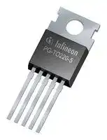
- Transistor Case Style: TO-220
- Drain Source Voltage Vds: 55V
- Operating Temperature Max: 175°C
- Continuous Drain Current Id: 35A
- Drain Source On State Resistance: 0.0115ohm
- Gate Source Threshold Voltage Max: 1.65V
| Delivery and price | |
|---|---|
| Units per pack | 100 |
| Price | 3.56 € |
| Current stock | 200+ |
| Lead time | 7 days |
**Speed TEMPFET BTS244Z**

## **Speed TEMPFET ®** N-Channel ° Enhancement mode ;

Enhancement mode

- Logic Level Input

- Analog driving possible

**==> picture [258 x 47] intentionally omitted <==**

**----- Start of picture text -----**<br>
1<br>1<br>5<br>5 PG-TO263-5-2 PG-TO220-5-12<br>**----- End of picture text -----**<br>


Fast switching up to 1 MHz

Potential-free temperature sensor with

- thyristor characteristics

- Overtemperature protection •

- Avalanche rated •

**Type** _V_ DS _R_ DS(on) **Package** ~~a~~ BTS244Z E3062A 55 V 13 m PG-TO263-5-2 BTS244Z E3043 PG-TO220-5-12 ~~| | *, ——+——— P| ee ee ee ee es~~ D Pin 3 and TAB ~~i ae~~ G Pin 1 A Pin 2 Temperature Sensor K Pin 4 S Pin 5

|Pin|Symbol|Function|
|---|---|---|
|1|G|Gate|
|2|A|Anode Temperature Sensor|
|3|D|Drain|
|4|K|Cathode Temperature Sensor|
|5|S|Source|


Data Sheet

1

Rev.1.4, 2013-07-26

**Speed TEMPFET BTS244Z**

|**Maximum Ratings**|~~ee~~|~~ee~~||
|---|---|---|---|
|**Parameter**|**Symbol**<br>~~ee~~|**Value**<br>~~ee~~|**Unit**|
|Drain source voltage<br>~~Q~~|_V_DS<br>~~ee~~<br>~~a~~<br>~~ee~~|55<br>~~ee~~<br>~~ee~~<br>~~ee~~|V|
|Drain-gate voltage,_R_GS= 20k<br>~~Q~~|_V_DGR<br>~~a ~~<br>~~ee~~|55<br> ~~ee~~<br>~~ee~~||
|Gate source voltage<br>~~Q~~|_V_GS<br>~~ee~~<br>~~ct~~|20<br>~~ee~~<br>~~ct~~||
|Nominal load current (ISO 10483)<br>_V_GS= 4.5 V,_V_DS<br>0.5 V,_T_C= 85 °C<br>_V_GS= 10 V,_V_DS<br>0.5 V,_T_C= 85 °C|_I_D(ISO)<br>~~ct~~|19<br>26<br>~~ct~~|A|
|Continuous drain current1)<br>_T_C= 100 °C,_V_GS= 4.5V|_I_D<br>~~Pf~~|35<br>~~Pf~~||
|Pulsed drain current|_I_D puls<br>~~a ~~|188<br> ~~eee~~||
|Avalanche energy, single pulse<br>_I_D= 19 A,_R_GS= 25<br>'|D puls<br>_E_AS<br>~~Sf~~|1.65<br>~~Sf~~|J|
|<br>Power dissipation<br>_T_C= 25 °C|_P_tot<br>~~Sf~~<br>~~ee~~|170<br>~~Sf~~<br>~~eee~~|W|
|<br>Operatingtemperature2)|_T_j<br>~~ee~~<br>~~ee~~|-40 ...+175<br>~~eee~~<br>~~ee~~|°C|
|Peak temperature ( single event )|j<br>_T_jpeak<br>~~ee ~~<br>~~ee~~|200<br> ~~eee~~<br>~~ee~~||
|Storage temperature|jpeak<br>_T_stg<br>~~ee~~<br>~~a ~~|-55 ... +150<br>~~ee~~<br> ~~ee~~||
|DIN humiditycategory, DIN 40 040|stg<br>~~a ~~<br>~~ee~~|E<br> ~~eee~~<br>~~ee~~||
|IEC climatic category; DIN IEC 68-1|~~ee~~|40/150/56<br>~~ee~~||


> 2Note: Thermal trip temperature of temperature sensor is below 175°C

1current limited by bond wire

Data Sheet

2

Rev.1.4, 2013-07-26

**Speed TEMPFET BTS244Z**

|**Thermal Characteristics**|
|---|
|**Parameter**<br>**Symbol**<br>**Values**<br>**Unit**<br>**min.**<br>**typ.**<br>**max.**<br>**Characteristics**<br>junction - case:<br>_R_thJC<br>-<br>-<br>0.88<br>K/W<br>Thermal resistance@min. footprint<br>_R_th(JA)<br>-<br>-<br>62<br>Thermal resistance@6 cm2coolingarea1)<br>_R_th(JA)<br>-<br>33<br>40<br>~~ee~~<br>~~**e**e~~<br>~~—— =~~|
|**Electrical Characteristics**|
|**Parameter**<br>**Symbol**<br>**Values**<br>**Unit**<br>at_T_j= 25°C, unless otherwise specified<br>**min.**<br>**typ.**<br>**max.**<br>**Static Characteristics**<br>~~ee eee~~|
|<br>Drain-source breakdown voltage<br>_V_GS= 0 V,_I_D= 0.25 mA<br>_V_(BR)DSS<br>55<br>-<br>-<br>V<br>Gate threshold voltage,_V_GS=_V_DS<br>_I_D= 130 μA<br>_I_D= 250 μA<br>_V_GS(th)<br>1.2<br>-<br>1.6<br>1.65<br>2<br>-<br>~~et~~<br>~~|~~<br>Core|
|Zero gate voltage drain current<br>_V_DS= 50 V,_V_GS= 0 V,_T_j= -40 °C<br>_V_DS= 50 V,_V_GS= 0 V,_T_j= 25 °C<br>_V_DS= 50 V,_V_GS= 0 V,_T_j= 150 °C<br>_I_DSS<br>-<br>-<br>-<br>-<br>0.1<br>-<br>0.1<br>1<br>100<br>μA<br>Baie|
|Gate-source leakage current<br>_V_GS= 20 V,_V_DS= 0 V,_T_j= 25 °C<br>_V_GS= 20 V,_V_DS= 0 V,_T_j= 150 °C<br>_I_GSS<br>-<br>-<br>10<br>20<br>100<br>100<br>nA<br>Drain-Source on-state resistance<br>_V_GS= 4.5 V,_I_D= 19 A<br>_V_GS= 10 V,_I_D= 19 A<br>_R_DS(on)<br>-<br>-<br>16<br>11.5<br>18<br>13<br>m<br>~~mann~~<br>~~CP~~|


> 1 Device on 50mm*50mm*1.5mm epoxy PCB FR4 with 6cm2 (one layer, 70μm thick) copper area for drain connection. PCB mounted vertical without blown air.

Data Sheet

3

Rev.1.4, 2013-07-26

**Speed TEMPFET BTS244Z**

**Electrical Characteristics**

|Forward transconductance<br>_V_DS>2*_I_D*_R_DS(on)max,_I_D= 35 A|_g_fs<br>~~ef~~|25<br>~~efff~~|-<br>~~ff~~|-<br>~~ff~~|S|
|---|---|---|---|---|---|
|Input capacitance<br>_V_GS= 0 V,_V_DS= 25 V,_f_= 1 MHz|_C_iss<br>~~ef~~<br>~~| ~~|-<br>~~ef ff~~<br> ~~ff~~|2130<br>~~ff~~<br>~~ff~~|2660<br>~~ff~~<br>~~ff~~|pF|
|Output capacitance<br>_V_GS= 0 V,_V_DS= 25 V,_f_= 1 MHz|_C_oss<br>~~| ~~|-<br> ~~ff~~|600<br>~~ff~~|750<br>~~ff~~||
|Reverse transfer capacitance<br>_V_GS= 0 V,_V_DS= 25 V,_f_= 1 MHz|_C_rss|-|320|400||
|<br>Turn-on delay time<br>_V_DD= 30 V,_V_GS= 4.5 V,_I_D= 47 A,<br>_R_G= 2.2|<br>_t_d(on)|-|15|25|ns|
|<br>Rise time<br>_V_DD= 30 V,_V_GS= 4.5 V,_I_D= 47 A,<br>_R_G= 2.2|<br>_t_r|-|70|105||
|Turn-off delay time<br>_V_DD= 30 V,_V_GS= 4.5 V,_I_D= 47 A,<br>_R_G= 2.2|_t_d(off)|-|40|60||
|Fall time<br>_V_DD= 30 V,_V_GS= 4.5 V,_I_D= 47 A,<br>_R_G= 2.2|_t_f|-|25|40||


Data Sheet

Rev.1.4, 2013-07-26

4

**Speed TEMPFET BTS244Z**

**==> picture [131 x 63] intentionally omitted <==**

## **Electrical Characteristics**

|**Electrical Characteristics**||||||
|---|---|---|---|---|---|
|**Parameter**<br>at_T_j= 25°C, unless otherwise specified|**Symbol**|**Values**|||**Unit**|
|||**min.**|**typ.**|**max.**||
|**Reverse Diode**||||||
|Inverse diode continuous forward current<br>_T_C= 25 °C|_I_S|35|-|-|A|
|Inverse diode direct current,pulsed<br>_T_C= 25 °C|_I_FM|188|-|-||
|Inverse diode forward voltage<br>_V_GS= 0 V,_I_F= 94 A|_V_SD|-|1.25|1.8|V|
|Reverse recovery time<br>_V_R= 30 V,_I_F=_I_S,d_i_F/d_t_= 100 A/μs|_t_rr|-|110|165|ns|
|Reverse recovery charge<br>_V_R= 30 V,_I_F=_I_S,d_i_F/d_t_= 100 A/μs|_Q_rr|-|0.23|0.35|μC|


## **Sensor Characteristics**

For temperature sensing, i.e. temperature protection, please consider application note "Temperature sense concept - Speed TEMPFET”.

For short circuit protection please consider application note "Short circuit behaviour of the Speed TEMPFET family”.

All application notes are available at **http://www.infineon.com/tempfet/**

|Forward voltage<br>_I_AK(on)= 5 mA,_T_j= -40...+150 °C<br>_I_AK(on)= 1.5 mA,_T_j= 150 °C<br>Sensor override<br>_t_P= 100 μs,_T_j= -40...+150 °C|_V_AK(on)|-<br>-|1.3<br>-|1.4<br>0.9|V|
|---|---|---|---|---|---|
|||-|-|10||
|Forward current<br>_T_j= -40...+150 °C<br>Sensor override<br>_t_P= 100 μs,_T_j= -40...+150 °C|_I_AK(on)|-|-|5|mA|
|||-|-|600||


Data Sheet

Rev.1.4, 2013-07-26

5

**Speed TEMPFET BTS244Z**

**==> picture [131 x 63] intentionally omitted <==**

## **Electrical Characteristics**

|**Electrical Characteristics**||||||
|---|---|---|---|---|---|
|**Parameter**<br>at_T_j= 25°C,unless otherwise specified|**Symbol**|**Values**|||**Unit**|
|||**min.**|**typ.**|**max.**||
|**Sensor Characteristics**||||||
|Temperature sensor leakage current<br>_T_j= 150 °C|_I_AK(off)|-|-|4|μA|
|Min. reset pulse duration1)<br>_T_j= -40...+150 °C,_I_AK(on)= 0.3 mA,<br>_V_AK(Reset)<0.5V|_t_reset|100|-|-|μs|
|_V_AKRecovery time1)2)<br>_T_j= -40...+150 °C,_I_AK(on)= 0.3 mA|_t_recovery|-|-|150||
|**Characteristics**||||||
|<br>Holding current, VAK(off)= 5V<br>_T_j= 25 °C<br>_T_j= 150 °C|_I_AK(hold)|0.05<br>0.05|-<br>-|0.5<br>0.3|mA|
|Thermal trip temperature<br>_V_TS= 5V|_T_TS(on)|150|160|170|°C|
|Turn-off time (Pin G+A and K+S connected)<br>_V_TS= 5V,_I_TS(on)= 2 mA|_t_off|0.5|-|2.5|μs|
|Reset voltage<br>_T_j= -40...+150°C|_V_AK(reset)|0.5|-|-|V|


## **Sensor recovery behaviour:**

**==> picture [135 x 138] intentionally omitted <==**

**----- Start of picture text -----**<br>
S e n s o r R E S E T<br>t re s e t<br>V A K [V ]<br>5<br>4<br>0<br>t<br>re c o v e ry<br>S e n s o r O N R e s e t O F F<br>**----- End of picture text -----**<br>


1See diagram Sensor recovery behaviour

2Time after reset pulse until VAK reaches 4V again

Data Sheet

6

Rev.1.4, 2013-07-26

**Speed TEMPFET BTS244Z**

## **1 Maximum allowable power dissipation Ptot = f(TC)**

## **2 Drain current**

_**I**_ **D = f(** _**T**_ **C);** _V_ GS = 4.5V

**==> picture [481 x 263] intentionally omitted <==**

**----- Start of picture text -----**<br>
180 | | | 40<br>A<br>crept EE ett<br>140<br>CUM 30 TL Ey<br>120<br>EET 25 PTX<br>EET PK<br>100<br>TTT TTI<br>20<br>80<br>15<br>60<br>10<br>40<br>20 5<br>0 0<br>-40 0 40 80 120 °C 180 0 20 40 60 80 100 120 140 °C 180<br>T C T C<br>tot<br>D<br>P I<br>**----- End of picture text -----**<br>


## **3 Typ. transient thermal impedance**

_**Z**_ **thJA=f(** _**t**_ **p) @ 6 cm[2] cooling area** Parameter: _D_ = _t_ / _T_ p

## **4 Transient thermal impedance**

## _Z_ thJC = _f_ ( _t_ p)

parameter : _D_ = _t_ p/ _T_

**==> picture [485 x 268] intentionally omitted <==**

**----- Start of picture text -----**<br>
10 2 10 1<br>K/W<br>K/W<br>a D=0.5 a alll 10 0 aae<br>10 1<br>D=0.5<br>0.2<br>0.2<br>0.1<br>10 -1 0.1<br>0.05<br>0.05<br>10 0<br>0.02<br>0.02<br>0.01 10 -2 0.01<br>SMe ee ae Sie See ee cae rama A<br>10 -1 HMA Single pulse  AN O 10 -3 e<br>Single pulse<br>10 -2 LITT 10 -4 Bu MU<br>TTI TTT UT A oo<br>10 [-5] 10 [-4] 10 [-3] 10 [-2] 10 [-1] 10 [0] 10 [1] s 10 [3] 10 [-8] 10 [-7] 10 [-6] 10 [-5] 10 [-4] 10 [-3] 10 [-2] 10 [-1] 10 [0] 10 [1] s 10 [3]<br>t t<br>p p<br>thJA thJC<br>Z Z<br>**----- End of picture text -----**<br>


Data Sheet

Rev.1.4, 2013-07-26

7

**Speed TEMPFET BTS244Z**

## **5 Safe operating area**

## _**I**_ **D=f(VDS);** _D_ =0.01; _T_ C=25°C

## **6 Typ. output characteristic**

## **ID = f(VDS);** Tj=25°C

Parameter: VGS

**==> picture [10 x 11] intentionally omitted <==**

**----- Start of picture text -----**<br>
D<br>I<br>**----- End of picture text -----**<br>


## **7 On-state resistance**

## _**R**_ **ON = f(Tj);** _I_ D=19A; _V_ GS = 4.5V

**==> picture [222 x 263] intentionally omitted <==**

**----- Start of picture text -----**<br>
180<br>A 10V<br>7V<br>140 6V<br>120<br>100<br>5V<br>s<br>80<br>4.5V<br>60<br>4V<br>40<br>3.5V<br>20 3V<br>0<br>0 < 1 2 = V 4<br>V DS<br>D<br>I<br>**----- End of picture text -----**<br>


## **8 On-state resistance**

## _**R**_ **ON = f(Tj);** _I_ D=19A; _V_ GS = 10V

**==> picture [481 x 262] intentionally omitted <==**

**----- Start of picture text -----**<br>
40 30<br>m<br>max. m<br>max.<br>HAT<br>30<br>25 typ. 20 typ.<br>Po ey KK<br>20 15<br>15 Eea<br>Se eet<br>10<br>10<br>Perec |  ET<br>5<br>PCAC<br>5<br>Poor LLL<br>0 0<br>-50 -25 0 25 50 75 100 125 °C 175 -50 -25 0 25 50 75 100 125 °C 175<br>T j T j<br>DS(on) DS(on)<br>R R<br>**----- End of picture text -----**<br>


Data Sheet

8

Rev.1.4, 2013-07-26

**Speed TEMPFET BTS244Z**

**==> picture [131 x 63] intentionally omitted <==**

## **9 Typ. transfer characteristics**

_**I**_ **D = f(** _**V**_ **GS);** _V_ DS = 12V; _T_ j = 25°C

## **10 Typ. input threshold voltage**

**VGS(th) = f(Tj);** _V_ DS= _V_ GS Parameter: _I_ D

**==> picture [488 x 268] intentionally omitted <==**

**----- Start of picture text -----**<br>
100 2.4<br>A V<br>2.0<br>80<br>1.8<br>70 130mA<br>1.6<br>60 13mA<br>1.4<br>50 1.2<br>1.3mA<br>40 1.0<br>0.8 130μA<br>30<br>0.6<br>20<br>0.4<br>10<br>0.2<br>0 0.0<br>0 1 2 3 V 5 -50 -25 0 25 50 75 100 125 °C 175<br>V GS T j<br>D GS(th)<br>I V<br>**----- End of picture text -----**<br>


## **11 Typ. capacitances**

_**C**_ **= f(** _**V**_ **DS);** _V_ GS=0 V, _f_ =1 MHz

## **12 Typ. forward charcteristics of**

## **reverse diode** _**I**_ **F = f(** _**V**_ **SD)**

_t_ p = 80μs (spread); Parameter: _T_ j

**==> picture [224 x 272] intentionally omitted <==**

**----- Start of picture text -----**<br>
10 1<br>nF<br>Ciss<br>10 0<br>Coss<br>Crss<br>10 -1<br>0 4 8 12 16 20 24 28 32 V 40<br>V DS<br>C<br>**----- End of picture text -----**<br>


**==> picture [228 x 272] intentionally omitted <==**

**----- Start of picture text -----**<br>
10 2<br>A<br>150°C<br>10 1 25°C<br>10 0<br>10 -1<br>0.0 0.2 0.4 0.6 0.8 1.0 1.2 V 1.6<br>V SD<br>F<br>I<br>**----- End of picture text -----**<br>


Data Sheet

9

Rev.1.4, 2013-07-26

**Speed TEMPFET BTS244Z**

**==> picture [131 x 63] intentionally omitted <==**

## **13 Typ. gate charge**

## _**V**_ **GS = f(** _**Q**_ **Gate);** _I_ D puls = 47A

**==> picture [228 x 274] intentionally omitted <==**

**----- Start of picture text -----**<br>
BTS 244 Z<br>16<br>V<br>12<br>10 0,2 V DS max<br>0,8 V DS max<br>8<br>6<br>4<br>2<br>0<br>0 20 40 60 80 100 nC 140<br>Q Gate<br>GS<br>V<br>**----- End of picture text -----**<br>


## **14 Drain-source break down voltage**

_V_ (BR)DSS = f( _T_ j)

**==> picture [229 x 267] intentionally omitted <==**

**----- Start of picture text -----**<br>
66<br>V<br>62<br>60<br>58<br>56<br>54<br>52<br>50<br>-40 0 40 80 120 °C 180<br>T<br>j<br>(BR)DSS<br>V<br>**----- End of picture text -----**<br>


Data Sheet

10

Rev.1.4, 2013-07-26

**Speed TEMPFET BTS244Z**

**==> picture [131 x 63] intentionally omitted <==**

## **Package Outlines**

## **1 Package Outlines**

**==> picture [497 x 607] intentionally omitted <==**

**----- Start of picture text -----**<br>
4.4<br>10 ±0.2<br>1.27 ±0.1<br>0...0.3<br>A B<br>8.5 1)<br>0.05<br>2.4<br>0.1<br>0...0.15<br>5 x 0.8 [±0.1]<br>4 x 1.7<br>0.25 [M] A B 0.1 B<br>1) Typical<br>Metal surface min. X = 7.25, Y = 6.9<br>All metal surfaces tin plated, except area of cut. GPT09062<br>Figure 1 PG-TO263-5-2<br>10 ±0.2<br>A<br>9.9 [±0.2] B<br>1)<br>8.5 4.4<br>3.7 -0.15 1.27 ±0.1<br>0...0.3<br>0.05<br>2.4<br>C<br>0...0.15 0.5 [±0.1]<br>5 x 0.8 ±0.1 2.4<br>4 x 1.7<br>0.25 [M] A B C<br>1) Typical<br>Metal surface min. X = 7.25, Y = 12.3<br>All metal surfaces tin plated, except area of cut.<br>8˚ MAX.<br>0.5 ±0.1<br>±0.3<br>1<br>1)<br>±0.2 ±0.3<br>) 7.55<br>(15 9.25 1.3 ±0.3<br>±0.5<br>2.7<br>4.7<br>±0.3 1) ±0.2<br>±0.3 12.95 2.8 ±0.2<br>17<br>15.65<br>9.25<br>±0.5 ±0.5<br>11<br>13<br>**----- End of picture text -----**<br>


**Figure 2 PG-TO220-5-12**

Data Sheet

11

Rev.1.4, 2013-07-26

**Speed TEMPFET BTS244Z**

**==> picture [131 x 63] intentionally omitted <==**

## **Package Outlines**

## **Green Product (RoHS compliant)**

To meet the world-wide customer requirements for environmentally friendly products and to be compliant with government regulations the device is available as a green product. Green products are RoHS-Compliant (i.e Pb-free finish on leads and suitable for Pb-free soldering according to IPC/JEDEC J-STD-020).

For further information on alternative packages, please visit our website: **http://www.infineon.com/packages** .

Dimensions in mm

Data Sheet

12

Rev.1.4, 2013-07-26

**Speed TEMPFET BTS244Z**

**==> picture [131 x 63] intentionally omitted <==**

## **Revision History**

## **2 Revision History**

|**Revision**|**Date**|**Changes**|
|---|---|---|
|1.4|2013-07-26|page 1, 11: updated package name and package drawing:<br>PG-TO220-5-62 to PG-TO263-5-2 (SMD)<br>PG-TO220-5-43 to PG-TO220-5-12 (THD, straight leads);<br>page 1, 11/12: removed package: PG-TO220-5-3 (THD, staggered leads)<br>page 1: added sales names for the different packages;<br>page 8: updated description figure 5|
|1.3|2009-12-04|updated package drawing of PG-TO220-5-62|
|1.2|2009-07-31|removed 100ms and DC line in SOA diagram|
|1.1|2008-11-10|all pages:<br>added new Infineon logo<br>Initial version of RoHS-compliant derivate of the BTS244Z<br>Page 1 and 12: added RoHS compliance statement and Green product feature<br>Page 1, 11 and 12: Package changed to RoHS compliant version<br>page 13: added Revision history<br>page 14: update of disclaimer|


Data Sheet

13

Rev.1.4, 2013-07-26

## **Edition 2013-07-26**

**Published by Infineon Technologies AG 81726 Munich, Germany © 2013 Infineon Technologies AG All Rights Reserved.**

## **Legal Disclaimer**

The information given in this document shall in no event be regarded as a guarantee of conditions or characteristics. With respect to any examples or hints given herein, any typical values stated herein and/or any information regarding the application of the device, Infineon Technologies hereby disclaims any and all warranties and liabilities of any kind, including without limitation, warranties of non-infringement of intellectual property rights of any third party.

## **Information**

For further information on technology, delivery terms and conditions and prices, please contact the nearest Infineon Technologies Office ( **www.infineon.com** ).

## **Warnings**

Due to technical requirements, components may contain dangerous substances. For information on the types in question, please contact the nearest Infineon Technologies Office.

Infineon Technologies components may be used in life-support devices or systems only with the express written approval of Infineon Technologies, if a failure of such components can reasonably be expected to cause the failure of that life-support device or system or to affect the safety or effectiveness of that device or system. Life support devices or systems are intended to be implanted in the human body or to support and/or maintain and sustain and/or protect human life. If they fail, it is reasonable to assume that the health of the user or other persons may be endangered.
Updated at March 10, 2026
Infineon Technologies is a globally recognized leader in semiconductor solutions, renowned for driving innovation in power management, energy efficiency, and modern mobility. With a strong legacy of engineering excellence, the company provides highly reliable components designed to meet the rigorous demands of industrial, automotive, and advanced commercial applications. The core of our Infineon portfolio is centered on their industry-leading discrete semiconductors. We offer an extensive selection of single and dual MOSFETs, alongside a robust range of single IGBTs and advanced IGBT modules. These flagship power transistors are essential for high-efficiency power conversion and motor control, providing engineers with superior thermal performance and minimized switching losses. Beyond advanced field-effect transistors, the selection includes a comprehensive array of diodes and rectifiers, heavily featuring Schottky diodes, as well as fast-recovery and RF/PIN diodes. This power foundation is further supported by bipolar transistors, intelligent power modules, and thyristor SCR modules, delivering the critical building blocks required for complex power system designs. To support broader system integration, the portfolio also encompasses specialized solutions such as solid-state relays, AC/DC LED driver ICs, and Bluetooth communications modules. From high-power industrial rectifiers to wireless connectivity adapters, Infineon equips designers with the precision components needed to build efficient, scalable, and fully connected electronic systems.
About Novapart
Novapart is a B2B electronic component broker specialising in stock shortages and cost reduction. We source hard-to-find parts and identify compliant alternatives across a catalogue of 410,000+ components from 500+ manufacturers.
Learn more →Stock Shortage Specialist
When a component is unavailable, discontinued or has an unacceptable lead time, we tap into our network of vetted European and Asian distributors to source what you need — without compromising on quality or traceability.
Request a quote →Compliant Alternatives
We identify pin-to-pin, electrically equivalent substitutes that meet the same certifications (RoHS, AEC-Q100, REACH) as your original specification — validated against datasheets, not just part numbers. Often at a lower cost.
BOM Analysis service →