
Image not available
Illustrative purposes only

BTHQ21608VSS-SRE
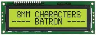
Alphanumeric LCD, 16 x 2, Black on Yellow / Green, 5V, Parallel, English, Japanese, Reflective
⚠️ Reference pricing provided. In case of supply shortages, we will connect you with our trusted procurement partners to ensure your project's continuity.
- Manufacturer: BATRON
- Product type: Alphanumeric LCD Displays
- Character Count x Line:16 x 2; Display Appearance:Black on Yellow / Green; Logic Voltage:5V; Interface Type:Parallel; Font Set:English, Japanese; Display Mode:Reflective; Character Size:9.
- Font Set: English, Japanese
- Module Size: 122mm x 43mm
- Display Mode: Reflective
- Logic Voltage: 5V
- Product Range: BTHQ21608VSS
- Character Size: 9.22mm
- Interface Type: Parallel
- LCD Display Type: STN
- Display Appearance: Black on Yellow / Green
- Backlighting Colour: No Backlight
- Display Construction: COB
- Character Count x Line: 16 x 2
- Operating Temperature Max: 50°C
- Operating Temperature Min: 0°C
| Delivery and price | |
|---|---|
| Units per pack | 100 |
| Price | 21.56 € |
| Current stock | 10+ |
| Lead time | 30 days |
Datasheet

**Feb/2002**

**1/12**

## _**BATRON**_

**BTHQ 21608VSS-SRE**

DOCUMENT NUMBER AND REVISION **VL-FS-BTHQ 21608VSS-01 REV.A (BTHQ 21608VSS-SRE)**

**BTHQ 21608VSS-SRE**

**2/12**

## _**BATRON**_

## REVISION HISTORY

|REVISION<br>FROM   TO|DATE||CHANGED<br>BY|CHECKED<br>BY|
|---|---|---|---|---|
|A|2002.01.04|First Release|PHILIP CHENG TOM LEE|PHILIP CHENG TOM LEE|


_**BATRON**_

**BTHQ 21608VSS-SRE**

**3/12**

## **CONTENTS**

||**CONTENTS**||
|---|---|---|
|||Page No.|
|1.|GENERAL  DESCRIPTION|4|
|2.|MECHANICAL  SPECIFICATIONS|4|
|3.|ABSOLUTE  MAXIMUM  RATINGS|6|
|3.1|ELECTRICAL  MAXIMUM  RATINGS (Ta=25°C)|6|
|3.2|ENVIRONMENTAL  CONDITION|6|
|4.|ELECTRICAL  SPECIFICATIONS|7|
|4.1|INTERFACE  SIGNALS|7|
|4.2|TYPICAL ELECTRICAL CHARACTERISTICS|8|
|4.3|TIMING SPECIFICATIONS|9|
|4.4|TIMING DIAGRAM OF VDD AGAINST V0|12|


_**BATRON**_

**BTHQ 21608VSS-SRE**

**4/12**

## **Specification of LCD Module Type ITEM NO.: BTHQ 21608VSS-01**

## **1. General Description**

- 16 characters (5 x 8 dots) x 2 lines STN Positive Yellow Reflective LCD Character Module.

- Viewing Angle: 6 o’clock direction.

- Driving scheme: 1/16 duty, 1/5 bias.

- ‘SAMSUNG’ KS0070BP-00CC (Die form) LCD Controller & Driver or equivalent.

## **2. Mechanical Specifications**

The mechanical detail is shown in Fig. 1 and summarized in Table 1 below.

Table 1

|Parameter|Specifications|Unit|
|---|---|---|
|Outline dimensions|122.0(W)x 43.0(H)x 11.0 MAX.(D)|mm|
|Effective viewingarea|99.0(W)x 23.0(H)|mm|
|Displayformat|16 characters x 2 lines|-|
|Character size|4.84(W)x 9.22(H) (5 x 8 dots)|mm|
|Character spacing|1.16(W)x 0.53(H)|mm|
|Characterpitch|6.00(W)x 9.75(H)|mm|
|Dot size|0.956(W)x 1.139(H)|mm|
|Dot spacing|0.015(W)x 0.015(H)|mm|
|Dotpitch|0.971(W)x 1.154(H)|mm|
|Weight:|TBD|Grams|


**BTHQ 21608VSS-SRE**

## _**BATRON**_

**5/12**

_**BATRON**_

**BTHQ 21608VSS-SRE**

**6/12**

## **3. Absolute Maximum Ratings**

## **3.1 Electrical Maximum Ratings(Ta = 25 ° C)**

Table 2

|Parameter|Symbol|Min.|Max.|Unit|
|---|---|---|---|---|
|Power Supplyvoltage(Logic)|VDD - VSS|-0.3|+7.0|V|
|Power Supplyvoltage(LCD drive)|VLCD=VDD – V0|-0.3|+15.0|V|
|Input voltage|Vin|-0.3|VDD+0.3|V|


Note:

The modules may be destroyed if they are used beyond the absolute maximum ratings. All voltage values are referenced to VSS = 0V.

## **3.2 Environmental Condition**

Table 3

|Item|Operating<br>Temperature<br>(Topr)|Operating<br>Temperature<br>(Topr)|Storage<br>Temperature<br>(Tstg)|Storage<br>Temperature<br>(Tstg)|Remark|
|---|---|---|---|---|---|
||Min.|Max.|Min.|Max.||
|Ambient Temperature|0°C|+50°C|-10°C|+60°C|Dry|
|Humidity|95% max. RH for Ta≤40°C<br>< 95%RH for Ta > 40°C||||no condensation|
|Vibration (IEC 68-2-6)<br>cells must be mounted<br>on a suitable connector|Frequency: 10∼55 Hz<br>Amplitude: 0.75 mm<br>Duration: 20 cycles in each direction.||||3 directions|
|Shock (IEC 68-2-27)<br>Half-sine pulse shape|Pulse duration : 11 ms<br>Peak acceleration: 981 m/s2 = 100g<br>Number of shocks:3 shocks in 3 mutually perpendicular axes.||||3 directions|


_**BATRON**_

**BTHQ 21608VSS-SRE**

**7/12**

## **4. Electrical Specifications**

## **4.1 Interface signals**

## Table 4

|||Table 4|
|---|---|---|
|Pin No.|Symbol|Description|
|1|VSS|Ground(0V).|
|2|VDD|Power supplyfor logic(+5.0V)|
|3|V0|Power supplyfor LCD driver|
|4|RS|Register Select Input:<br>”High’ for Data register (for read and write)<br>”Low” for Instruction register (for write),<br>Busyflag,address counter(for read)|
|5|R/W|Read/Write signal:<br>‘High’ for Read mode.<br>‘Low’ for Write mode.|
|6|E|Enable.<br>Start signal for data read /write.|
|7|DB0|Data input/output(LSB)|
|8|DB1|Data input/output|
|9|DB2|Data input/output|
|10|DB3|Data input/output|
|11|DB4|Data input/output|
|12|DB5|Data input/output|
|13|DB6|Data input/output|
|14|DB7|Data input/output(MSB)|
|A|LED(+)|Anode of LED Backlight.|
|K|LED(-)|Cathode of LED Backlight.|


_**BATRON**_

**BTHQ 21608VSS-SRE**

**8/12**

## **4.2 Typical Electrical Characteristics**

**At Ta = +25 ° C, VDD = +5V ± 5%, VSS = 0V.**

## Table 5

|||Table 5|||||
|---|---|---|---|---|---|---|
|Parameter|Symbol|Conditions|Min.|Typ.|Max.|Unit|
|Supplyvoltage(Logic)|VDD-VSS||4.75|5.0|5.25|V|
|Supply voltage (LCD)|VLCD<br>=VDD-V0|VDD = 5V,<br>Note 1|4.0|4.5|5.0|V|
|Input signal voltage 1<br>for E,DB0-DB7,R/W,RS|VIH1|“High” level|2.2|-|VDD|V|
||VIL1|“Low” level|-0.3|-|0.6|V|
|Input signal voltage 2<br>for OSC1|VIH2|“High” level|VDD -1.0|-|VDD|V|
||VIL2|“Low” level|-|-|1.0|V|
|Supply Current<br>(Logic & LCD)|IDD|Character mode,<br>Note 1|-|1.7|2.6|mA|
|Supply Current (LCD)|I0|Character mode,<br>Note 1|-|0.9|1.4|mA|


## Note (1):

There is tolerance in optimum LCD driving voltage during production and it will be within the specified range.

_**BATRON**_

**BTHQ 21608VSS-SRE**

**9/12**

## **4.3 Timing Specifications**

At Ta = 0 °C to +50 °C , VDD = 5V±5%, VSS=0V.

Refer to Fig. 2, the bus timing diagram for write mode.

|Table 6|Table 6|Table 6|Table 6|Table 6|Table 6|
|---|---|---|---|---|---|
|~~eG~~||||||
|Parameter<br>~~Re~~|Symbol<br>~~Re~~<br>~~eG~~|Min.<br>~~Re~~<br>~~eG~~|Max.<br>~~Re~~|Unit<br>~~Re~~|Testpin<br>~~Re~~|
|E cycle time<br>~~ee~~|tC<br>~~eG~~<br>~~ee~~|500<br>~~eG~~<br>~~ee~~|-<br>~~ee~~|ns<br>~~ee~~|E<br>~~ee~~|
|E rise time<br>~~ee~~|tR<br>~~ee~~|-<br>~~ee~~|25<br>~~ee~~|ns<br>~~ee~~|E<br>~~ee~~|
|E fall time<br>~~Re~~|tF<br>~~Re~~|-<br>~~Re~~|25<br>~~Re~~|ns<br>~~Re~~|E<br>~~Re~~|
|Epulse width(High,Low)<br>~~ee~~|tW<br>~~ee~~|220<br>~~ee~~|-<br>~~ee~~|ns<br>~~ee~~|E<br>~~ee~~|
|R/W and RS set-uptime<br>~~eG~~|tSU1<br>~~eG~~|40<br>~~eG~~|-<br>~~eG~~|ns<br>~~eG~~|R/W,RS<br>~~eG~~|
|R/W and RS hold time<br>~~ee~~|tH1<br>~~ee~~|10<br>~~ee~~|-<br>~~ee~~|ns<br>~~ee~~|R/W,RS<br>~~ee~~|
|Data set-uptime<br>~~eG~~|tSU2<br>~~eG~~|60<br>~~eG~~|-<br>~~eG~~|ns<br>~~eG~~|DB0-DB7<br>~~eG~~|
|Data hold time<br>~~a~~|tH2|10|-|ns|DB0-DB7|


## Refer to Fig. 3, the bus timing diagram for read mode.

|Table 7|Table 7|Table 7|Table 7|Table 7|Table 7|
|---|---|---|---|---|---|
|||||||
|Parameter<br>~~es~~|Symbol<br>~~es~~|Min.<br>~~es~~|Max.<br>~~es~~|Unit<br>~~es~~|Testpin<br>~~es~~|
|E cycle time<br>~~eG~~|tC<br>~~eG~~|500<br>~~eG~~|-<br>~~eG~~|ns<br>~~eG~~|E<br>~~eG~~|
|E rise time<br>~~ee~~|tR<br>~~ee~~|-<br>~~ee~~|25<br>~~ee~~|ns<br>~~ee~~|E<br>~~ee~~|
|E fall time<br>~~eG~~|tF<br>~~eG~~|-<br>~~eG~~|25<br>~~eG~~|ns<br>~~eG~~|E<br>~~eG~~|
|Epulse width<br>~~es~~|tW<br>~~es~~|220<br>~~es~~|-<br>~~es~~|ns<br>~~es~~|E<br>~~es~~|
|R/W and RS set-uptime<br>~~es~~|tSU<br>~~es~~|40<br>~~es~~|-<br>~~es~~|ns<br>~~es~~|R/W,RS<br>~~es~~|
|R/W and RS hold time<br>~~Re~~|tH<br>~~Re~~|10<br>~~Re~~|-<br>~~Re~~|ns<br>~~Re~~|R/W,RS<br>~~Re~~|
|Data output delaytime<br>~~ee~~|tD<br>~~ee~~|-<br>~~ee~~|120<br>~~ee~~|ns<br>~~ee~~|DB0-DB7<br>~~ee~~|
|Data hold time<br>~~eG~~|tDH<br>~~eG~~|20<br>~~eG~~|-<br>~~eG~~|ns<br>~~eG~~|DB0-DB7<br>~~eG~~|


_**BATRON**_

**BTHQ 21608VSS-SRE**

**10/12**

Figure 2: The bus timing diagram for write mode .

_**BATRON**_

**BTHQ 21608VSS-SRE**

**11/12**

Figure 3: The bus timing diagram for read mode .

_**BATRON**_

**BTHQ 21608VSS-SRE**

**12/12**

## **4.4  Timing Diagram of VDD against V0.**

Power on sequence shall meet the requirement of Figure 4, the timing diagram of VDD against V0.

**==> picture [457 x 458] intentionally omitted <==**

**----- Start of picture text -----**<br>
VDD<br>95%<br>LOGIC SUPPLY<br>VOLTAGE<br>0V<br>50ms(typical)<br>OV<br>LCD SUPPLY<br>VOLTAGE<br>V0<br>**----- End of picture text -----**<br>


Figure 4: Timing diagram of VDD against V0.
Updated at June 10, 2026
About Novapart
Novapart is a B2B electronic component broker specialising in stock shortages and cost reduction. We source hard-to-find parts and identify compliant alternatives across a catalogue of 410,000+ components from 500+ manufacturers.
Learn more →Stock Shortage Specialist
When a component is unavailable, discontinued or has an unacceptable lead time, we tap into our network of vetted European and Asian distributors to source what you need — without compromising on quality or traceability.
Request a quote →Compliant Alternatives
We identify pin-to-pin, electrically equivalent substitutes that meet the same certifications (RoHS, AEC-Q100, REACH) as your original specification — validated against datasheets, not just part numbers. Often at a lower cost.
BOM Analysis service →