


BTA41-600BRG
Triac, 600 V, 40 A, TOP-3, 1.3 V, 400 A, 80 mA
- Manufacturer: STMICROELECTRONICS
- Product type:
- Peak Repetitive Off-State Voltage, Vdrm:600V; On State RMS Current IT(rms):40A; Triac Case Style:TOP-3; Gate Trigger Current Max (QI), Igt:50mA; Gate Trigger Voltage Max Vgt:1.3V; Peak Gate Power
- MSL: -
- SVHC: No SVHC (25-Jun-2025)
- No. of Pins: 3Pins
- Product Range: -
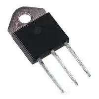
- Triac Case Style: TOP-3
- Thyristor Mounting: Through Hole
- Holding Current Max: 80mA
- On State RMS Current: 40A
- Peak On State Voltage: 1.55V
- Gate Trigger Voltage Max: 1.3V
- Operating Temperature Max: 125°C
- Peak Non Repetitive Surge Current: 400A
- Peak Repetitive Off State Voltage: 600V
| Delivery and price | |
|---|---|
| Units per pack | 100 |
| Price | 4.13 € |
| Current stock | 1000+ |
| Lead time | 30 days |
**BTA40, BTA41, BTB41**

Datasheet

## 800 V and 600 V, 40 A standard Triacs in TOP3 and RD91 package

**==> picture [131 x 164] intentionally omitted <==**

**----- Start of picture text -----**<br>
A2<br>G<br>A1<br>A1<br>G A2<br>RD91<br>A2<br>A1 A1<br>A2 G A2 G<br>TOP3 Isolated TOP3<br>**----- End of picture text -----**<br>


## **Features**

- High current Triac

- Low thermal resistance

- BTA40 and BTA41 UL1557 recognized components (file ref: 81734)

- RoHS (2002/95/EC) compliant packages

- UL-94, V0 flammability package resin compliance

## **Applications**

- On/off function in static relays, heating regulation, induction motor starting circuits

- Phase control operations in light dimmers and motor speed controllers

## **Description**

Available in power packages, the BTA40, BTA41 and BTB41 are suitable for general purpose AC switching.

When used with the properly dimensioned heatsink, the BTA40, BTA41 and BTB41 can enable AC switching systems up to 9 kW. Refer to ST Application Note AN533 for thermal management of Triacs.

The BTA40, BTA41 and BTB41 provides an insulated tab (rated at 2500 V rms). They are recognized by UL. Representative samples of these components have been evaluated by UL and meet applicable UL requirements for UL 1557 standard (File Ref. 81734).

|**Product status link**|**Product status link**|
|---|---|
|BTA40|RD91 package|
|BTA41|TOP3 isolated<br>package|
|BTB41|TOP3 package|
|||
|**Product summary**||
|**IT(RMS)**|40 A|
|**VDRM/VRRM**|600 V to 800 V|
|**IGT**|50 mA|


**DS2111** - **Rev 11** - **March 2021** For further information contact your local STMicroelectronics sales office.

www.st.com

**BTA40, BTA41, BTB41 Characteristics**

## **1 Characteristics**

**Table 1. Absolute maximum ratings**

|**Symbol**|**Parameters**|||**Value**|**Unit**|
|---|---|---|---|---|---|
|IT(RMS)|RMS on-state current (180° conduction angle)|BTA40, BTA41|Tc= 80 °C|40|A|
|||BTB41|Tc= 95 °C|||
|ITSM|Non repetitive surge peak on-state current (full cycle, Tjinitial = 25 °C)||tp= 16,7 ms|420|A|
||||tp= 20 ms|400||
|I2t|I2t value for fusing|tp= 10 ms||1000|A2s|
|dl/dt|Critical rate of rise of on-state current<br>IG= 2 x IGT, tr≤ 100 ns|f = 120 Hz|Tj= 125 °C|50|A/µs|
|VDSM, VRSM|Non repetitive surge peak off-state voltage|tp= 20 ms|Tj= 25 °C|VDRM, VRRM+ 100|V|
|IGM|Peak gate current|tp= 20 µs|Tj= 125 °C|8|A|
|PG(AV)|Average gate power dissipation||Tj= 125 °C|1|W|
|Tstg|Storage junction temperature range|||-40 to +150|°C|
|Tj|Operating junction temperature range|||-40 to +125|°C|


**Table 2. Electrical characteristics (Tj = 25 °C, unless otherwise specified) - standard (4 quadrants)**

|**Symbol**|**Parameters**|**Quadrant**||**Values**|**Unit**|
|---|---|---|---|---|---|
|IGT(1)|VD= 12 V, RL= 33 Ω|I - II - III<br>IV|Max.|50<br>100|mA|
|VGT||I - II - III|Max.|1.3|V|
|VGD|VD= VDRM, RL= 3.3 kΩ, Tj= 125 °C|I - II - III|Min.|0.2|V|
|IH(2)|IT= 500 mA||Max.|80|mA|
|IL|IG= 1.2 IGT|I - III - IV|Max.|70|mA|
|||II|Max.|160||
|dV/dt(2)|VD= 67 % VDRMgate open, Tj= 125 °C||Min.|500|V/µs|
|(dV/dt)c(2)|(dI/dt)c = 20 A/ms, Tj= 125 °C||Min.|10|V/µs|


_1. Minimum IGT is guaranteed at 5 % of IGT max._

_2. For both polarities of A2 referenced to A1_

**Table 3. Static electrical characteristics**

|**Symbol**|**Test conditions**|**Tj**||**Value**|**Unit**|
|---|---|---|---|---|---|
|VTM(1)|ITM= 60 A, tp= 380 µs|25 °C|Max.|1.55|V|
|VTO(1)|threshold on-state voltage|125 °C|Max.|0.85|V|
|RD(1)|Dynamic resistance|125 °C|Max.|10|mΩ|
|IDRM/IRRM|VT= VDRM, VT= VRRM|25 °C|Max.|5|µA|
|||125 °C||5|mA|


_1. For both polarities of A2 referenced to A1_

**DS2111** - **Rev 11**

**page 2/12**

**BTA40, BTA41, BTB41 Characteristics**

## **Table 4. Thermal resistance**

|**Symbol**|**Parameters**|**Parameters**|**Value**|**Unit**|
|---|---|---|---|---|
|Rth(j-c)|Junction to case (AC)|BTA40 / BTA41|0.9|°C/W|
|||BTB41|0.6||
|Rth(j-a)|Junction to ambient|BTA40 / BTA41 / BTB41|50||


**DS2111** - **Rev 11**

**page 3/12**

**BTA40, BTA41, BTB41 Characteristics (curves)**

## **1.1 Characteristics (curves)**

**==> picture [513 x 401] intentionally omitted <==**

**----- Start of picture text -----**<br>
Figure 1. Maximum power dissipation versus on-state Figure 2. RMS on-state current versus case temperature<br>RMS current (full cycle) (full cycle)<br>P(W)<br>50 IT(RMS)(A)<br>45<br>α=180°<br>40<br>40<br>BTB41<br>35 BTA40<br>BTA41<br>30 30<br>25<br>20 20<br>180° 15<br>10 α<br>10<br>α<br>IT(RMS) (A) 5 TC(°C)<br>0<br>0 5 10 15 20 25 30 35 40 0<br>0 25 50 75 100 125<br>Figure 3. Relative variation of thermal impedance versus<br>Figure 4. On-state characteristics (maximum values)<br>pulse duration<br>K=[Z th/Rth] 400 ITM(A)<br>1.E+00<br>Tj max.<br>Zth(j-c) Vto = 0.85V<br>Rd = 10 mΩ<br>100<br>[T] j [= T] j [max.]<br>1.E-01<br>Zth(j-a)<br>BTA / BTB41<br>Tj = 25°C.<br>10<br>1.E-02<br>VTM(V)<br>1<br>1.E-03 tp(s) 0.5 1.0 1.5 2.0 2.5 3.0 3.5 4.0 4.5 5.0<br>1.E-03 1.E-02 1.E-01 1.E+00 1.E+01 1.E+02 1.E+03<br>**----- End of picture text -----**<br>


**Figure 5. Surge peak on-state current versus number of Figure 6. Non-repetitive surge peak on-state current for a cycles sinusoidal pulse**

**==> picture [477 x 137] intentionally omitted <==**

**----- Start of picture text -----**<br>
ITSM (A) ITSM(A), I²t (A²s)<br>450 10000<br>400 dI/dt limitation:50A/µs ITSM Pulse width tp < 10 msTj initial=25 °C<br>350 t=20ms<br>Non repetitive<br>300 Tj initial=25°C One cycle 1000<br>250<br>200<br>150 Repetitive<br>TC=70°C<br>100<br>50<br>0 Number of cycles 100 tp(ms)<br>1 10 100 1000<br>0.01 0.10 1.00 10.00<br>**----- End of picture text -----**<br>


**DS2111** - **Rev 11**

**page 4/12**

**BTA40, BTA41, BTB41 Characteristics (curves)**

**Figure 7. Relative variation of gate trigger current, holding Figure 8. Relative variation of critical rate of decrease of and latching current versus junction temperature main current versus (dV/dt)c (typical values)**

**==> picture [479 x 134] intentionally omitted <==**

**----- Start of picture text -----**<br>
IGT,IH,IL[T ] /j IGT,IH,IL[Tj=25°C] (dI/dt)c [(dV/dt)c] / specified (dI/dt)c<br>2.5 2.0<br>1.8<br>2.0<br>1.6<br>IGT<br>1.5 1.4<br>IH & IL Typical values 1.2<br>1.0 1.0<br>0.8<br>0.5<br>0.6<br>Tj(°C) (dV/dt)c (V/µs)<br>0.0 0.4<br>-40 -20 0 20 40 60 80 100 120 140 0.1 1.0 10.0 100.0<br>**----- End of picture text -----**<br>


**Figure 9. Relative variation of critical rate of decrease of main current versus junction temperature (typical values)**

**==> picture [222 x 132] intentionally omitted <==**

**----- Start of picture text -----**<br>
(dI/dt)c [Tj ] / (dI/dt)c [Tj specified]<br>6<br>5<br>4<br>3<br>2<br>1<br>Tj(°C)<br>0<br>0 25 50 75 100 125<br>**----- End of picture text -----**<br>


**DS2111** - **Rev 11**

**page 5/12**

**BTA40, BTA41, BTB41 Package information**

**2 Package information**

In order to meet environmental requirements, ST offers these devices in different grades of ECOPACK packages, depending on their level of environmental compliance. ECOPACK specifications, grade definitions and product status are available at: www.st.com. ECOPACK is an ST trademark.

## **2.1 TOP3 insulated and non-insulated package information**

- Epoxy meets UL94, V0

- Lead-free packages

- Recommended torque: 1.05 N·m (max. torque: 1.2 N·m)

## **Figure 10. TOP3 insulated and non-insulated package outline**

**==> picture [312 x 371] intentionally omitted <==**

**DS2111** - **Rev 11**

**page 6/12**

**BTA40, BTA41, BTB41 TOP3 insulated and non-insulated package information**

**Table 5. TOP3 insulated and non-insulated mechanical data**

||**Dimensions**|**Dimensions**|**Dimensions**|**Dimensions**|**Dimensions**|**Dimensions**|
|---|---|---|---|---|---|---|
|**Ref.**|**mm**|||**Inches(1)**|||
||**Min.**|**Typ.**|**Max.**|**Min.**|**Typ.**|**Max.**|
|A|4.40||4.60|0.1732||0.1812|
|B|1.45||1.55|0.0570||0.0611|
|C|14.35||15.60|0.5649||0.6142|
|D|0.50||0.70|0.0196||0.0276|
|E|2.70||2.90|0.1062||0.1142|
|F|15.80||16.50|0.6220||0.6497|
|G|20.40||21.10|0.8031||0.8308|
|H|15.10||15.50|0.5944||0.6103|
|J|5.40||5.65|0.2125||0.2225|
|K|3.40||3.65|0.1338||0.1438|
|L|4.08||4.17|0.1606||0.1642|
|M|1.20||1.40|0.0472||0.0552|
|R||4.60|||0.1811||


_1. Inches given for reference only_

**DS2111** - **Rev 11**

**page 7/12**

**BTA40, BTA41, BTB41 RD91 package information**

## **2.2 RD91 package information**

- Epoxy meets UL94, V0

- Cooling method: Conduction

- Recommended torque: 0.9 to 1.2 N·m

## **Figure 11. RD91 package outline**

**==> picture [395 x 453] intentionally omitted <==**

**----- Start of picture text -----**<br>
A2<br>L2 E L1<br>B2<br>B1<br>C<br>C2 C1<br>A1<br>N1<br>N2<br>B<br>F<br>E3<br>I<br>A<br>E2<br>**----- End of picture text -----**<br>


**DS2111** - **Rev 11**

**page 8/12**

**BTA40, BTA41, BTB41 RD91 package information**

## **Table 6. RD91 mechanical data**

||**Dimensions**|**Dimensions**|**Dimensions**|**Dimensions**|**Dimensions**|**Dimensions**|
|---|---|---|---|---|---|---|
|**Ref.**|**mm**|||**Inches(1)**|||
||**Min.**|**Typ.**|**Max.**|**Min.**|**Typ.**|**Max.**|
|A|||40.00|||1.575|
|A1|30.10||30.30|1.185||1.193|
|A2|||22.00|||0.867|
|B|||27.00|||1.063|
|B1|13.50||16.50|0.531||0.650|
|B2|||24.00|||0.945|
|C|||14.00|||0.552|
|C1|||3.50|||0.138|
|C2|1.90||2.10|0.074||0.083|
|E|6.10||6.50|0.240||0.256|
|E2|4.80||5.20|0.188||0.205|
|E3|0.70||0.90|0.027||0.036|
|F|4.00||4.30|0.157||0.170|
|I|11.20||11.60|0.440||0.536|
|L1|3.10||3.50|0.122||0.138|
|L2|1.70||1.90|0.066||0.075|
|N1|33°||43°|33°||43°|
|N2|28°||38°|28°||38°|


_1. Inches given for reference only_

**DS2111** - **Rev 11**

**page 9/12**

**BTA40, BTA41, BTB41 Ordering information**

## **3**

## **Ordering information**

**Figure 12. Ordering information scheme (BTA40, BTA41 and BTB-41 series)**

**==> picture [357 x 247] intentionally omitted <==**

**----- Start of picture text -----**<br>
BT    A    40  -  600       B     RG<br>Triac series<br>Insulation<br>A = Insulated<br>B = Non-insulated<br>Current<br>40 = 40 A in RD91<br>41 = 40 A in TOP3 or TOP3 insulated<br>Voltage<br>600 = 600 V<br>800 = 800 V<br>Sensitive and type<br>B = 50 mA standard<br>Package<br>RG = Tube<br>Blank = Bulk<br>**----- End of picture text -----**<br>


**Table 7. Ordering information**

|**Order code**|**Marking**|**Package**|**Weight**|**Base qty.**|**Delivery mode**|
|---|---|---|---|---|---|
|BTA40-600B|BTA40600B|RD91|20 g|25|Bulk|
|BTA40-800B|BTA40800B|RD91|20 g|25|Bulk|
|BTA41-600BRG|BTA41600B|TOP3 Ins.|4.5 g|30|Tube|
|BTA41-800BRG|BTA41800B|TOP3 Ins.|4.5 g|30|Tube|
|BTB41-600BRG|BTB41600B|TOP3|4.5 g|30|Tube|
|BTB41-800BRG|BTB41800B|TOP3|4.5 g|30|Tube|


**DS2111** - **Rev 11**

**page 10/12**

**BTA40, BTA41, BTB41**

## **Revision history**

**Table 8. Document revision history**

|**Date**|**Revision**|**Changes**|
|---|---|---|
|Sep-2003|5|Last update.|
|25-Mar-2005|6|TOP3 delivery mode changed from bulk to tube.|
|14-Oct-2005|7|Tcvalues for ITchanged in Table 3. ECOPACK statement added.|
|10-Aug-2009|8|Updated Table 2 to correctly place packages. Updated Figure 2. Table 5<br>changed to correctly place TOP3.<br>Updated ECOPACK statement.|
|02-Dec-2020|9|UpdatedFigure 6andFigure 12. Added Application section. Minor text<br>change.|
|28-Jan-2021|10|UpdatedTable 1andTable 4.|
|24-Mar-2021|11|Updated coverimage.|


**DS2111** - **Rev 11**

**page 11/12**

**BTA40, BTA41, BTB41**

## **IMPORTANT NOTICE – PLEASE READ CAREFULLY**

STMicroelectronics NV and its subsidiaries (“ST”) reserve the right to make changes, corrections, enhancements, modifications, and improvements to ST products and/or to this document at any time without notice. Purchasers should obtain the latest relevant information on ST products before placing orders. ST products are sold pursuant to ST’s terms and conditions of sale in place at the time of order acknowledgement.

Purchasers are solely responsible for the choice, selection, and use of ST products and ST assumes no liability for application assistance or the design of Purchasers’ products.

No license, express or implied, to any intellectual property right is granted by ST herein.

Resale of ST products with provisions different from the information set forth herein shall void any warranty granted by ST for such product.

ST and the ST logo are trademarks of ST. For additional information about ST trademarks, please refer to www.st.com/trademarks. All other product or service names are the property of their respective owners.

Information in this document supersedes and replaces information previously supplied in any prior versions of this document.

© 2021 STMicroelectronics – All rights reserved

**DS2111** - **Rev 11**

**page 12/12**
Updated at June 10, 2026
STMicroelectronics is a global leader in the semiconductor industry, recognized for developing highly integrated, energy-efficient solutions that power modern electronics. With a strong focus on innovation, ST provides a comprehensive portfolio of microelectronics that address the demanding requirements of industrial, automotive, communications, and consumer applications. Our extensive selection of STMicroelectronics components is built around a robust lineup of discrete semiconductors and circuit protection devices. We offer a wide variety of single MOSFETs, Schottky diodes, and fast and ultrafast recovery rectifier diodes, designed to deliver exceptional efficiency and thermal performance in power management and conversion systems. For robust circuit protection, our inventory features hundreds of transient voltage suppressors and TVS diodes that safeguard sensitive electronic components against destructive voltage spikes. In addition to core power discretes like TRIACs, SCRs, bipolar transistors, and single IGBTs, our STMicroelectronics range includes specialized integrated passive filters and MEMS sensors. Furthermore, ST offers advanced integrated passive devices, such as baluns and RF filters, which utilize high-quality monolithic RF IPD processes on glass or high-resistance silicon substrates. These components provide competitive cost structures, reduced power losses, and simplified RFIC-to-antenna matching, ensuring optimal system performance and delivering the reliability required for next-generation wireless and power designs.
About Novapart
Novapart is a B2B electronic component broker specialising in stock shortages and cost reduction. We source hard-to-find parts and identify compliant alternatives across a catalogue of 410,000+ components from 500+ manufacturers.
Learn more →Stock Shortage Specialist
When a component is unavailable, discontinued or has an unacceptable lead time, we tap into our network of vetted European and Asian distributors to source what you need — without compromising on quality or traceability.
Request a quote →Compliant Alternatives
We identify pin-to-pin, electrically equivalent substitutes that meet the same certifications (RoHS, AEC-Q100, REACH) as your original specification — validated against datasheets, not just part numbers. Often at a lower cost.
BOM Analysis service →