


BSS83PH6327XTSA1
Power MOSFET, P Channel, 60 V, 330 mA, 2 ohm, SOT-23, Surface Mount
- Manufacturer: INFINEON
- Product type: Single MOSFETs
- Transistor Polarity:P Channel; Continuous Drain Current Id:-330mA; Drain Source Voltage Vds:-60V; On Resistance Rds(on):1.4ohm; Rds(on) Test Voltage Vgs:-10V; Threshold Voltage Vgs:-
- MSL: -
- SVHC: No SVHC (25-Jun-2025)
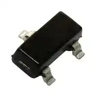
- No. of Pins: 3Pins
- Channel Type: P Channel
- Product Range: -
- Qualification: AEC-Q101
- Power Dissipation: 360mW
- Transistor Mounting: Surface Mount
- Rds(on) Test Voltage: 10V
- Transistor Case Style: SOT-23
- Drain Source Voltage Vds: 60V
- Operating Temperature Max: 150°C
- Continuous Drain Current Id: 330mA
- Drain Source On State Resistance: 2ohm
- Gate Source Threshold Voltage Max: 1.5V
| Delivery and price | |
|---|---|
| Units per pack | 5000 |
| Price | 0.071 € |
| Current stock | 50+ |
| Lead time | 30 days |
**BSS 83 P** ## **SIPMOS**[] **Small-Signal-Transistor** ## **Features** |**SIPMOS**[] **Small-Signal-Transistor**<br>**Features**||||| |---|---|---|---|---| |**Features**<br>**Product Summary**||||| |P-Channel<br>Drain source voltage|VDS<br>-60||V|| |Enhancement mode<br>Drain-source on-state resistance<br>RDS(on)<br>2|||W|| |Avalanche rated<br>Continuous drain current|A<br>ID<br>-0.33|||| |Logic Level<br>dv/dt rated<br>• Qualified according to AEC Q101<br>• Halogen-free according to IEC61249-2-21<br>¢Pb-freeleadplating;ROHScompliant<br>@®Halogen-Free<br>Z—!/~<br>RoHS|1<br>2<br>3<br>VPS05161<br>SEae<br>~<br>A|||| |**Type**<br>**Package**<br>**Tape and Reel**<br>**Marking**|**Pin 1**<br>**PIN 2**||**PIN 3**|**PIN 3**| |BSS 83 P<br>PG-SOT-23 H<br>6327: 3000pcs/r.<br>YAs|G<br>S||D|| |**Maximum Ratings**,at Tj= 25 °C, unless otherwise specified||||| |**Parameter**<br>**Symbol**<br>**Value**<br>-0.33<br>-0.27<br>Continuous drain current<br>TA= 25 °C<br>TA= 70 °C<br>ID<br>rf|||**Unit**<br>A|| |Pulsed drain current<br>ID puls|-1.32|||| |TA= 25 °C||||| |Avalanche energy, single pulse<br>EAS|9.5||mJ|| |ID= -0.33 A , VDD= -25 V, RGS= 25W||||| |Avalanche energy, periodic limited by Tjmax<br>EAR|0.036|||| |dv/dt<br>6<br>Reverse diode dv/dt<br>IS= -0.33 A, VDS= -48 V, di/dt = 200 A/µs,<br>Tjmax= 150 °C<br>Gate source voltage<br>VGS<br>20<br>Power dissipation<br>TA= 25 °C<br>Ptot<br>0.36<br>Operating and storage temperature<br>Tj ,Tstg<br>-55...+150<br>IEC climatic category; DIN IEC 68-1<br>55/150/56<br>ESD Class; JESD22-A114-HBM<br>Class 0<br>PfTT<br>ee eee<br>~~ee~~<br>ee<br>~~i~~|||kV/µs<br>V<br>W<br>°C|| - ¢ Pb-free Qualified according to AEC Q101 lead plating; ROHS compliant - Halogen-free according to IEC61249-2-21 2014-07-07 Rev. 1.6 Page 1 **BSS 83 P** **Thermal Characteristics** |**Thermal Characteristics**|||||| |---|---|---|---|---|---| |**Parameter**<br>**Characteristics**<br>~~ee ~~|**Symbol**<br>|**Unit**<br>**Values**<br>**min.**<br>**max.**<br>**typ.**<br> ~~ee~~|||| |Thermal resistance, junction - soldering point|RthJS|-|-|150|K/W| |( Pin 3 )|||||| |SMD version, device on PCB:|RthJA||||| |@ min. footprint||-|-|350|| |@ 6 cm2cooling area1)||-|-|300|| |Drain- source breakdown voltage<br>VGS= 0 V, ID= -250 µA<br>||V(BR)DSS<br>||<br>S||-60<br>**|**<br>S|tt|-<br>tt|-<br>tt|V| |---|---|---|---|---|---| |Gate threshold voltage, VGS= VDS<br>ID= -80 µA<br>||VGS(th)<br>| |<br>S||-1<br>**|**<br>S|tt|-1.5<br>tt|-2<br>tt|| |Zero gate voltage drain current<br>VDS= -60 V, VGS= 0 V, Tj= 25 °C<br>VDS= -60 V, VGS= 0 V, Tj= 125 °C<br>||IDSS<br>S|<br>tty<br>|||-<br>-<br>S| tt<br>tty<br>**|**|-0.1<br>-10<br>tt<br>tty|-1<br>-100<br>tt<br>tty|µA| |Gate-source leakage current<br>VGS= -20 V, VDS= 0 V<br>|<br>||IGSS<br>||<br>|||-<br>**|**<br>**|**|-10|-100|nA| |Drain-source on-state resistance<br>VGS= -4.5 V, ID= -0.27 A<br>|<br>||RDS(on)<br>| |<br>||<br>pt|-<br>**|**<br>**|**<br>pttt|2<br>tt|3<br>tt|W| |Drain-source on-state resistance<br>VGS= -10 V, ID= -0.33 A<br>||RDS(on)<br>| |<br>pt|-<br>**|**<br>pttt|1.4<br>tt|2<br>tt|| 1Device on 40mm*40mm*1.5mm epoxy PCB FR4 with 6cm2 (one layer, 70 µm thick) copper area for drain connection. PCB is vertical without blown air. 2014-07-07 Rev. 1.6 Page 2 |**Dynamic Characteristics**|||||| |---|---|---|---|---|---| |Transconductance<br>VDS 2*ID*RDS(on)max, ID= -0.27 A<br>.<br>_|gfs<br>| <br>_<br>||0.24<br> tt<br>ft|0.47<br>tt<br>ft|-<br>tt<br>ft|S| |Input capacitance<br>VGS= 0 V, VDS= -25 V, f = 1 MHz<br>_<br>_|Ciss<br>_<br>|<br>_<br>||-<br>ft<br>tt|62<br>ft<br>tt|78<br>ft<br>tt|pF| |Output capacitance<br>VGS= 0 V, VDS= -25 V, f = 1 MHz<br>_<br>_|Coss<br>_<br>|<br>_<br>||-<br>ft<br>tt|19<br>ft<br>tt|24<br>ft<br>tt|| |Reverse transfer capacitance<br>VGS= 0 V, VDS= -25 V, f = 1 MHz<br>_|Crss<br>_<br>||-<br>tt|7<br>tt|9<br>tt|| |Turn-on delay time<br>VDD= -30 V, VGS= -4.5 V, ID= -0.27 A,<br>RG= 43W|td(on)|-|23|35|ns| |Rise time<br>VDD= -30 V, VGS= -4.5 V, ID= -0.27 A,<br>RG= 43W|tr|-|71|106|| |Turn-off delay time<br>VDD= -30 V, VGS= -4.5 V, ID= -0.27 A,<br>RG= 43W|td(off)|-|56|70|| |Fall time<br>VDD= -30 V, VGS= -4.5 V, ID= -0.27 A,<br>RG= 43W|tf|-|61|76|| 2014-07-07 Rev. 1.6 Page 3 |**BSS 83 P**<br>**Electrical Characteristics,**at Tj= 25 °C, unless otherwise specified<br>**Unit**<br>**Values**<br>**Symbol**<br>**Parameter**<br>**min.**<br>**typ.**<br>**max.**<br>Gafineone~~e~~|**BSS 83 P**<br>**Electrical Characteristics,**at Tj= 25 °C, unless otherwise specified<br>**Unit**<br>**Values**<br>**Symbol**<br>**Parameter**<br>**min.**<br>**typ.**<br>**max.**<br>Gafineone~~e~~|**BSS 83 P**<br>**Electrical Characteristics,**at Tj= 25 °C, unless otherwise specified<br>**Unit**<br>**Values**<br>**Symbol**<br>**Parameter**<br>**min.**<br>**typ.**<br>**max.**<br>Gafineone~~e~~|**BSS 83 P**<br>**Electrical Characteristics,**at Tj= 25 °C, unless otherwise specified<br>**Unit**<br>**Values**<br>**Symbol**<br>**Parameter**<br>**min.**<br>**typ.**<br>**max.**<br>Gafineone~~e~~|**BSS 83 P**<br>**Electrical Characteristics,**at Tj= 25 °C, unless otherwise specified<br>**Unit**<br>**Values**<br>**Symbol**<br>**Parameter**<br>**min.**<br>**typ.**<br>**max.**<br>Gafineone~~e~~|**BSS 83 P**<br>**Electrical Characteristics,**at Tj= 25 °C, unless otherwise specified<br>**Unit**<br>**Values**<br>**Symbol**<br>**Parameter**<br>**min.**<br>**typ.**<br>**max.**<br>Gafineone~~e~~| |---|---|---|---|---|---| |**Dynamic Characteristics**|||||| |Gate to source charge|Qgs|-|0.12|0.18|nC| |VDD= -48 V, ID= -0.33 A|||||| |Gate to drain charge|Qgd|-|1.1|1.65|| |VDD= -48 , ID= -0.33 A|||||| |Gate charge total|Qg|-|2.38|3.57|| |VDD= -48 V, ID= -0.33 A, VGS= 0 to -10 V|||||| |Gate plateau voltage|V(plateau)|-|-2.94|-|V| |VDD= -48 V , ID= -0.33 A|||||| **Parameter Symbol Values Unit min. typ. max.** ~~ce~~ **Reverse Diode** Inverse diode continuous forward current IS - - -0.33 A TA = 25 °C ~~pt~~ Inverse diode direct current,pulsed ISM - - -1.32 TA = 25 °C |tt Inverse diode forward voltage _ VSD - | -0.84 -1.1 V VGS = 0 V, IF = -0.33 of - Reverse recovery time trr 59.4 89 ns VR = -30 V, IF=IS , diF/dt = 80 A/µs Reverse recovery charge pf} Qrr -[tt] | 37.5 56 nC VR = -30 V, IF=lS , diF/dt = 80 A/µs | tf 2014-07-07 Rev. 1.6 Page 4 **BSS 83 P** ## **Power Dissipation** ## Ptot = f (TA) ## **Drain current** ## ID = f (TA) ## parameter: VGS > 10 V **==> picture [268 x 270] intentionally omitted <==** **----- Start of picture text -----**<br> BSS 83 P<br>0.38 COLT<br>W<br>Sek Gs00000000000<br>0.32<br>PLEA T TT Ey ty tt eT<br>Ptt TAPE ETT Et<br>0.28<br>Lit tAt HEE TT<br>HIN<br>0.24 NEEREEEEE<br>CCCCCEENC EH]<br>0.20<br>0.16<br>} ceeFCCP AAA<br>SNe<br>0.12 FTP tee XL<br>PEPE<br>0.08 FCCC EEN<br>FCCC<br>0.04 FCCP<br>COC<br>0.00<br>0 20 40 60 80 100 120 °C 160<br>TA<br>tot<br>D<br>P I<br>**----- End of picture text -----**<br> **==> picture [28 x 5] intentionally omitted <==** **----- Start of picture text -----**<br> BSS 83 P<br>**----- End of picture text -----**<br> **==> picture [227 x 259] intentionally omitted <==** **----- Start of picture text -----**<br> -0.36 A E CONERE<br>-0.28 CCCCPREECEEE<br>A EPTTEN EEE<br>FCCC Ee<br>-0.24<br>SEEEECEES EE<br>-0.20 CECE ~EEE<br>-0.16<br>EEENene<br>-0.12 PTTPTT TTTTTT TTTEEE TTEe TNTYE TE<br>-0.08 EEEEEE ECEEEA<br>EEE EEE<br>-0.04 EEE<br>OCCA<br>0.00<br>0 20 40 60 80 100 120 °C 160<br>TA<br>D<br>I<br>**----- End of picture text -----**<br> ## **Safe operating area** ID = f ( VDS ) ## parameter : D = 0 , TA = 25 °C **==> picture [237 x 271] intentionally omitted <==** **----- Start of picture text -----**<br> BSS 83 P<br>-10 1<br>A rt tT TTT TET<br>a tp = 88.0µs<br>-10 0 100 µs<br>o r<br>| tT | TNT ATT<br> 1 ms<br>-10 -1 gf SCHIST<br> 10 ms<br>rt tT TTT TTR EET<br>a Nl<br>-10 -2<br>DC<br>rt tT Tt TET<br>a ee el<br>-10 -3 a a il<br>-10 [-1 ] -10 [0 ] -10 [1 ] V -10 [2 ]<br>—r VDS<br>I D<br> /<br>V DS<br> =<br>D R DS(on)<br>I<br>**----- End of picture text -----**<br> ## **Transient thermal impedance** ## ZthJC = f (tp) ## parameter : D = tp/T **==> picture [235 x 273] intentionally omitted <==** **----- Start of picture text -----**<br> BSS 83 P<br>10 3<br>K/W a a a a<br>a AN a<br>10 2<br>CPST UT<br>me em A<br>10 1 SE RTTTHT<br>D = 0.50<br>eS 0.20 tt<br>HIATT SSH RCA TH 0.100.05 Ul<br>10 0<br>single pulse 0.02<br>0.01<br>CALI TMT UTI TTT TTT TI TIT T tt<br>PARA) RR<br>10 -1 TINT TAIT TTT<br>10 [-5 ] 10 [-4 ] 10 [-3 ] 10 [-2 ] 10 [-1 ] 10 [0 ] 10 [1 ] 10 [2 ] s 10 [4 ]<br>—r tp<br>thJC<br>Z<br>**----- End of picture text -----**<br> 2014-07-07 Rev. 1.6 Page 5 **BSS 83 P** ## **Typ. output characteristic** ID = f (VDS); Tj=25°C parameter: tp = 80 µs **==> picture [230 x 271] intentionally omitted <==** **----- Start of picture text -----**<br> BSS 83 P<br>-0.80 Ptot = 0W<br>A yi jhikglf e d tt tt tt VGS [V] ty<br>SSeeeen a -2.5<br>b -3.0<br>a) (sn<br>-0.60<br>c -3.5<br>on) (An d -4.0<br>c<br>-0.50 fo(s./ ef -4.5-5.0<br>g -5.5<br>BL<br>-0.40 h -6.0<br>pho i -6.5<br>-0.30 5 AS j -7.0<br>b k -8.0<br>0 |e Seeeeeee<br>l -10.0<br>ff<br>-0.20<br>| Aa Zs<br>-0.10 | ar ne a ee<br>Ane<br>0.00<br>0.0 -0.5 -1.0 -1.5 -2.0 -2.5 -3.0 -3.5 -4.0 V -5.0<br>VDS<br>D<br>I<br>**----- End of picture text -----**<br> ## **Typ. drain-source-on-resistance** RDS(on) = f (ID) parameter: VGS **==> picture [233 x 270] intentionally omitted <==** **----- Start of picture text -----**<br> BSS 83 P<br>6.5<br>W a b c<br>can PT ety Ei<br>5.5<br>CE<br>5.0 EEE EE<br>4.5 TEL EE EL<br>PELLET<br>4.0 I<br>3.5<br>TEL PAL TLE TT<br>3.0 Sae7annnen/ien<br>2.52.0 eeTetTE<br>| Eber LL d<br>1.5 l f e<br>treet ttl tee j h kig ||<br>eee<br>1.0<br>VGS [V] =<br>a b c d e f g h i j k l<br>0.5 -2.5 -3.0 -3.5 -4.0 -4.5 -5.0 -5.5 -6.0 -6.5 -7.0 -8.0 -10.0<br>0.0<br>0.00 -0.10 -0.20 -0.30 -0.40 -0.50 A -0.65<br>ID<br>DS(on)<br>R<br>**----- End of picture text -----**<br> ## **Typ. transfer characteristics** ID= f ( VGS ) VDS 2 x ID x RDS(on)max parameter: tp = 80 µs ## **Typ. forward transconductance** gfs = f(ID); Tj=25°C parameter: gfs **==> picture [486 x 261] intentionally omitted <==** **----- Start of picture text -----**<br> -1.2 0.70<br>A S<br>EEE 0.60<br>-1.0<br>-0.9 PLETE LT/ALL 0.55 PEIde<br>0.50<br>Seeeeeeeseee PEt eT<br>-0.8<br>0.45<br>TTT T PEt tT yar<br>-0.7 0.40 PTTL TALT ETE<br>-0.6 0.35<br>fete Ty ee PCOOALCEEEL<br>-0.5 0.30<br>Reece ot 0.25 Sececet<br>-0.4<br>0.20<br>SeGeen4eeee A7EEEAE<br>-0.3<br>0.15<br>Se eeEeeneeee ACCA<br>-0.2<br>0.10<br>-0.1 te / 0.05 WEEE TTT EEE ELL<br>0.0 PLL ttTALYE TTEELttLL 0.00 P FET TEOEEE [PEELE] C<br>0.0 -1.0 -2.0 -3.0 -4.0 V -6.0 0.00 -0.10 -0.20 -0.30 -0.40 -0.50 A -0.70<br>VGS ID<br>ID gfs<br>**----- End of picture text -----**<br> 2014-07-07 Rev. 1.6 Page 6 **BSS 83 P** ## **Drain-source on-state resistance** ## RDS(on) = f (Tj) parameter : ID = -0.33 A, VGS = -10 V ## **Gate threshold voltage** ## V GS(th) = f (Tj) parameter: VGS = VDS, ID = -80 µA **==> picture [28 x 5] intentionally omitted <==** **----- Start of picture text -----**<br> BSS 83 P<br>**----- End of picture text -----**<br> **==> picture [485 x 599] intentionally omitted <==** **----- Start of picture text -----**<br> 5.5 -3.0<br>W<br>TOA V qqyyy<br>COOP<br>4.5<br>4.0 98%<br>Pere TT<br>-2.0<br>3.5 COPE oan<br>3.0 typ<br>COO AL<br>-1.5<br>98%<br>2.5<br>SURRREEEGERE Sep SEEL<br>2.0 2%<br>P CC typ errr tf -1.0 BLT<br>1.5<br>CEE erry ae<br>1.0 reer ee<br>-0.5<br>0.5<br>CT PEPEPEP EEE<br>0.0 0.0<br>-60 -20 20 60 100 °C 180 -60 -20 20 60 100 °C 160<br>—r Tj —_r Tj<br>Typ. capacitances Forward characteristics of reverse diode<br>C = f (VDS) IF = f (VSD)<br>parameter: VGS=0V, f=1 MHz p = 80 µs<br>parameter: Tj , t<br>BSS 83 P<br>10 3 -10 1<br>SC CECE<br>pF ——— ee A<br>es ee ee ee PLT ETT ETT ETT tT<br>10 2 -10 0<br>pt a ee<br>——— aa Ciss =<<br>1 a es<br> Coss<br>| 10 1 ——— -10 -1 en 6/AReeeeeeee<br>SL POET<br> Crss Tj = 25 °C typ<br>—SSeE SAS ==<br>Tj = 150 °C typ<br>a aS Tj = 25 °C (98%) a<br>ee ee it Tj = 150 °C (98%) || tT<br>10 0 -10 -2<br>0 et -5 -10 tt -15 -20 ty -25 yt V -35 0.0 q -0.4 -0.8 -1.2 e -1.6 -2.0 -2.4 V -3.0<br>. VDS . VSD<br>DS(on) GS(th)<br>R V<br>F<br>C I<br>**----- End of picture text -----**<br> ## **Forward characteristics of reverse diode** Rev. 1.6 Page 7 2014-07-07 **BSS 83 P** ## **Avalanche energy** ## EAS = f (Tj) para.: ID = -0.33 A , VDD = -25 V, RGS = 25 ## **Typ. gate charge** VGS = f (QGate) parameter: ID = -0.33 A pulsed BSS 83 P **==> picture [228 x 263] intentionally omitted <==** **----- Start of picture text -----**<br> 10<br> mJ<br>hE tT Tt<br>8 NERPY] Fy 7 fy<br>7<br>KEPT<br>6<br>TTC<br>5<br>Ty AT TT fd<br>4<br>3 eTaNIN | ff<br>2<br>FT NTT<br>1<br>NS<br>0 ae<br>25 45 65 85 105 125 °C 165<br> Tj<br>AS<br> E<br>**----- End of picture text -----**<br> **==> picture [228 x 262] intentionally omitted <==** **----- Start of picture text -----**<br> -16<br>V PLHHH ELT ELEEL ELLHEH E<br>SSR 0S0R000 407.08<br>-12<br>PT EL ELELELILVELALL<br>Ji |<br>-10 FEEEEEEEEAAEAT<br>FEEEEEELYC EEE<br>-8<br>BGGGG80 4070000008<br>-6 0,2 VDS max 0,8 VDS max<br>chPOOL av4auuD CE a<br>-4<br>PIL ELIZALVYE LE LEE<br>-2 pA<br>PEEL ELL EEE LEE<br>0 PLETE ELEET ELE ELE<br>0.0 0.4 0.8 1.2 1.6 2.0 2.4 2.8 nC 3.4<br>QGate<br>GS<br>V<br>**----- End of picture text -----**<br> ## **Drain-source breakdown voltage** V(BR)DSS = f (Tj) **==> picture [230 x 273] intentionally omitted <==** **----- Start of picture text -----**<br> BSS 83 P<br>-72 rf | | | | | ft tt yf<br>V rt | | | ft tt ty<br>rt | | | ft tt ty<br>-68 rtrf || || ft| fttt ttte tttyPe<br>-66 Pt tT tt | tt<br>Pt tf<br>-64 rtP| |ftte|| ete|| || te|| teYTPT Pa eTtf<br>ee Ane<br>-62 FELEE ALLL ei<br>-60 PitFt} tAPATtettT Eyttye<br>-58 |rt Ytiwi| ft| || tt| ttttft flfl<br>-56 YtZ| | || || || || || ft| fttttf<br>-54 rt | | | | | | tt tT<br>-60 -20 20 60 100 °C 180<br>T<br>j<br>(BR)DSS<br>V<br>**----- End of picture text -----**<br> Rev. 1.6 Page 8 2014-07-07 **BSS83P** **Package Outline:** ## **Footprint:** **Packaging:** Rev 1.6 page 9 2014-07-07 **BSS 83 P** ## **Published by** ## **Infineon Technologies AG 81726 Munich, Germany © 2010 Infineon Technologies AG All Rights Reserved.** ## **Legal Disclaimer** The information given in this document shall in no event be regarded as a guarantee of conditions or characteristics. With respect to any examples or hints given herein, any typical values stated herein and/or any information regarding the application of the device, Infineon Technologies hereby disclaims any and all warranties and liabilities of any kind, including without limitation, warranties of non-infringement of intellectual property rights of any third party. ## **Information** For further information on technology, delivery terms and conditions and prices, please contact the nearest Infineon Technologies Office (www.infineon.com). ## **Warnings** Due to technical requirements, components may contain dangerous substances. For information on the types in question, please contact the nearest Infineon Technologies Office. Infineon Technologies components may be used in life-support devices or systems only with the express written approval of Infineon Technologies, if a failure of such components can reasonably be expected to cause the failure of that life-support device or system or to affect the safety or effectiveness of that device or system. Life support devices or systems are intended to be implanted in the human body or to support and/or maintain and sustain and/or protect human life. If they fail, it is reasonable to assume that the health of the user or other persons may be endangered. 2014-07-07 Rev. 1.6 Page 10
Updated at April 29, 2026
Infineon Technologies is a globally recognized leader in semiconductor solutions, renowned for driving innovation in power management, energy efficiency, and modern mobility. With a strong legacy of engineering excellence, the company provides highly reliable components designed to meet the rigorous demands of industrial, automotive, and advanced commercial applications. The core of our Infineon portfolio is centered on their industry-leading discrete semiconductors. We offer an extensive selection of single and dual MOSFETs, alongside a robust range of single IGBTs and advanced IGBT modules. These flagship power transistors are essential for high-efficiency power conversion and motor control, providing engineers with superior thermal performance and minimized switching losses. Beyond advanced field-effect transistors, the selection includes a comprehensive array of diodes and rectifiers, heavily featuring Schottky diodes, as well as fast-recovery and RF/PIN diodes. This power foundation is further supported by bipolar transistors, intelligent power modules, and thyristor SCR modules, delivering the critical building blocks required for complex power system designs. To support broader system integration, the portfolio also encompasses specialized solutions such as solid-state relays, AC/DC LED driver ICs, and Bluetooth communications modules. From high-power industrial rectifiers to wireless connectivity adapters, Infineon equips designers with the precision components needed to build efficient, scalable, and fully connected electronic systems.
About Novapart
Novapart is a B2B electronic component broker specialising in stock shortages and cost reduction. We source hard-to-find parts and identify compliant alternatives across a catalogue of 410,000+ components from 500+ manufacturers.
Learn more →Stock Shortage Specialist
When a component is unavailable, discontinued or has an unacceptable lead time, we tap into our network of vetted European and Asian distributors to source what you need — without compromising on quality or traceability.
Request a quote →Compliant Alternatives
We identify pin-to-pin, electrically equivalent substitutes that meet the same certifications (RoHS, AEC-Q100, REACH) as your original specification — validated against datasheets, not just part numbers. Often at a lower cost.
BOM Analysis service →