


BSS138IXTSA1
Power MOSFET, N Channel, 60 V, 230 mA, 3.5 ohm, SOT-23, Surface Mount
- Manufacturer: INFINEON
- Product type: Single MOSFETs
- MSL: MSL 1 - Unlimited
- SVHC: No SVHC (25-Jun-2025)
- No. of Pins: 3Pins
- Channel Type: N Channel
- Product Range: -
- Qualification: -
- Power Dissipation: 360mW
- Transistor Mounting: Surface Mount
- Rds(on) Test Voltage: 10V
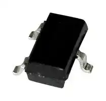
- Transistor Case Style: SOT-23
- Drain Source Voltage Vds: 60V
- Operating Temperature Max: 150°C
- Continuous Drain Current Id: 230mA
- Drain Source On State Resistance: 3.5ohm
- Gate Source Threshold Voltage Max: 1V
| Delivery and price | |
|---|---|
| Units per pack | 1500 |
| Price | 0.053 € |
| Current stock | 500+ |
| Lead time | 30 days |
om. Cinfineone@

BSS138!

## Small ~~-S~~ ignal Transistor

## Features

¢ N ~~-~~ channel

- e« Enhancement mode

- Logic level

- ¢ dv/dt rated

* Pb ~~-f~~ ree lead ~~-p~~ lating; ROHS compliant * Halogen free according to IEC61249 ~~-2-2~~ 1

**==> picture [63 x 107] intentionally omitted <==**

**----- Start of picture text -----**<br>
PG - SOT23 -3<br>3<br>]<br>1<br>y<br>2<br>**----- End of picture text -----**<br>


## Product validation

Fully qualified according to JEDEC for Industrial Applications

~~Table 1. | Key Performance Parameters~~

**==> picture [30 x 28] intentionally omitted <==**

**----- Start of picture text -----**<br>
Drain<br>Pin3<br>O E<br>**----- End of picture text -----**<br>


ESD Sensitivity,

**==> picture [83 x 36] intentionally omitted <==**

**----- Start of picture text -----**<br>
@ ROHS<br>**----- End of picture text -----**<br>


Final Data Sheet

1

Rev ~~.~~ 2 ~~.~~ 1, 2021 ~~-0~~ 3 ~~-~~ 17

**==> picture [121 x 53] intentionally omitted <==**

**==> picture [167 x 165] intentionally omitted <==**

Small ~~-S~~ ignal ~~BSS138I Transistor~~

Tnfit ~~C~~ in neon ;

1 Maximum ratings at Ta=25 °C, unless otherwise specified

## ~~Table 2_—/ Maximum ratings~~

|~~Table2_—/ Maximum~~|~~2_—/ Maximum Maximum~~|~~2_—/ Maximum Maximumratings~~|~~ratings~~|~~ratings~~|~~ratings~~|~~ratings~~|~~ratings~~|~~ratings~~|~~ratings~~|
|---|---|---|---|---|---|---|---|---|---|
|~~Table 2_—/ Maximum Maximum ratings~~<br>~~p~~~~**aramet**~~<br>~~Symbol,~~<br>~~er~~<br>~~Continuousdraincurrent~~<br>~~»~~||||~~Symbol,~~<br>~~ymbo~~<br>~~Min.~~<br>~~»Ff~~|~~Symbol,ae~~<br>~~Min.|~~<br>~~Typ.[Max._~~|||~~it~~|~~NoITe~~~~**s**t~~<br>~~Condit~~<br>~~ote /Te t~~<br>~~Condition~~<br>~~aeC~~|
||||||~~Symbol,ae~~<br>~~Min.|~~<br>~~Typ.~~<br>~~Ff~~|~~ae~~<br>~~|~~<br>~~Typ.[Max._~~<br>~~Ff~~|~~[Max._~~<br>~~oa~~|||
|~~p~~~~**aramet**~~<br>~~Symbol,~~<br>~~er~~<br>~~Continuousdraincurrent~~<br>~~»~~||||~~Symbol,~~<br>~~ymbo~~<br>~~Min.~~<br>~~»Ff~~|~~Symbol, ae~~<br>~~Min. |~~<br>~~Typ.~~<br>~~Ff~~|~~ae~~<br>~~|~~<br>~~Typ. [Max._~~<br>~~Ff~~|~~[Max._~~<br>~~oa~~|~~it ~~|~~No I Te~~~~**s**t~~<br>~~Condit~~<br>~~ote / Te t~~<br>~~Condition~~<br>~~aeC~~|
|~~Continuous drain current~~<br>~~»~~<br>~~Reversediodedv/dt~~||||~~» Ff~~<br>~~dvidt~~<br>~~-~~|~~Ff~~<br>~~-b~~|~~Ff~~<br>~~be~~|~~oa~~<br>~~e|~~|~~kV/us~~|~~ae C~~<br>~~pr0.2eoe48V,di/dt=200A/us,~~|
|~~Reversediodedv/dt~~||||~~dvidt~~<br>~~-~~|~~-b~~|~~be~~|~~e|~~|~~kV/us~~|~~pr0.2eoe48V,di/dt=200A/us,~~<br>j,max—|
|~~Reverse diode dv/dt~~||||~~dvidt~~<br>~~-~~|~~- b~~|~~be~~|~~e | ~~|~~kV/us ~~|~~pr0.2e oe48 V, di/dt=200 A/us,~~|
|~~Operatingandstoragetemperature~~<br>~~Tit~~||||~~Tit~~<br>~~(65~~|~~(65|~~|~~|~~<br>~~itso~~|~~itso~~|~~eo~~|~~BINreas.eee~~|
|~~Operatingandstoragetemperature~~<br>~~Tit~~||||~~Tit~~<br>~~(65~~|~~(65|~~|~~|~~<br>~~itso~~|~~itso~~|~~eo~~|~~BINreas.eee~~|


## 2 Thermal characteristics

## Table 3. Thermal characteristics

|Table 3.|Thermal characteristics|characteristics|characteristics|characteristics|characteristics|characteristics|characteristics|characteristics|characteristics|
|---|---|---|---|---|---|---|---|---|---|
|~~p~~~~**aramet**~~<br>~~symbol,~~<br>~~er~~||||~~symbol,~~<br>~~ymbo~~<br>~~Min.~~|~~symbol,ae~~<br>~~nit~~<br>~~Min._|~~<br>~~Typ.[Max._~~|||~~nit~~|~~N~~~~**o**|Te~~~~**s**t~~<br>~~Condit~~<br>~~te /Te t~~<br>~~Condition~~|
||||||~~symbol,ae~~<br>~~Min._|~~<br>~~Typ.~~|~~ae~~<br>~~_|~~<br>~~Typ.[Max._~~|~~nit~~<br>~~[Max._~~|||
|~~p~~~~**aramet**~~<br>~~symbol,~~<br>~~er~~<br>Thermal resistance, junction ~~- ~~minimal||||~~symbol,~~<br>~~ymbo~~<br>~~Min.~~|~~symbol, ae~~<br>~~Min._|~~<br>~~Typ.~~|~~ae~~<br>~~_|~~<br>~~Typ. [Max._~~|~~nit~~<br>~~[Max._~~|~~nit ~~|~~N~~~~**o** | Te~~~~**s**t~~<br>~~Condit~~<br>~~te / Te t~~<br>~~Condition~~|


## 3 Electrical characteristics

at Tj=25 °C, unless otherwise specified

## Table 4 Static characteristics

|Table 4|Static|Static characteristics|characteristics|characteristics|characteristics|characteristics|characteristics|characteristics|characteristics|
|---|---|---|---|---|---|---|---|---|---|
|~~p~~~~**aramet**~~<br>~~Symbol,~~<br>~~er~~<br>~~Drain-sourcebreakdownvoltage~~<br>~~lVaross~~||||~~Symbol,~~<br>~~ymbo~~<br>~~Min.~~<br>~~lVaross~~<br>~~[60~~|~~Symbol,ae~~<br>~~Min._|~~<br>~~Typ.[Max._~~|||~~it~~<br>~~|v~~|~~No|Te~~~~**s**t~~<br>~~Condit~~<br>~~ote /Te t~~<br>~~Condition~~<br>~~Ves=0V,Ip=250UA~~|
||||||~~Symbol,ae~~<br>~~Min._|~~<br>~~Typ.~~<br>~~[60|-~~|~~ae~~<br>~~_|~~<br>~~Typ.[Max._~~<br>~~|- |-~~|~~[Max._~~<br>~~|-|v~~|||
|~~p~~~~**aramet**~~<br>~~Symbol,~~<br>~~er~~<br>~~Drain-sourcebreakdownvoltage~~<br>~~lVaross~~<br>~~Gatethresholdvoltage~~<br>~~Vosm~~||||~~Symbol,~~<br>~~ymbo~~<br>~~Min.~~<br>~~lVaross~~<br>~~[60~~<br>~~Vosm~~<br>~~«(06~~|~~Symbol, ae~~<br>~~Min._|~~<br>~~Typ.~~<br>~~[60|-~~<br>~~«(06=[1.0~~|~~ae~~<br>~~_|~~<br>~~Typ. [Max._~~<br>~~|- |-~~<br>~~[1.0(14~~|~~[Max._~~<br>~~|-|v~~<br>~~(14[Vv~~|~~it ~~<br>~~|v~~<br>~~[Vv~~|~~No | Te~~~~**s**t~~<br>~~Condit~~<br>~~ote / Te t~~<br>~~Condition~~<br>~~Ves=0V,Ip=250UA~~<br>~~Ves=Vobs,[p=26YA~~|
|~~Drain-source breakdown voltage~~<br>~~lVaross~~<br>~~Gatethresholdvoltage~~<br>~~Vosm~~||||~~lVaross~~<br>~~[60~~<br>~~Vosm~~<br>~~«(06~~|~~[60 |-~~<br>~~«(06=[1.0~~|~~|-  |-~~<br>~~[1.0(14~~|~~|- |v~~<br>~~(14[Vv~~|~~|v ~~<br>~~[Vv~~|~~Ves= 0 V, Ip=250 UA~~<br>~~Ves=Vobs,[p=26YA~~|
|~~Gate threshold voltage~~<br>~~Vosm~~<br>.<br>~~ee~~<br>~~Gate-sourceleakagecurrent~~<br>~~ess~~||||~~Vosm~~<br>~~«(06~~<br>~~ee~~<br>~~essse~~|~~«(06 = [1.0~~<br>~~ee~~<br>~~se~~|~~[1.0 (14~~<br>~~ee~~|~~(14 [Vv~~<br>0~~.~~1<br>~~ee~~<br>~~10[nc~~|~~[Vv ~~<br>~~ee~~<br>~~[nc~~|~~Ves=Vobs, [p=26 YA~~<br>Vos=60 V,Ves=0 V, Tj=25 °C<br>~~ee~~<br>~~Ves=20V,Vos=0V~~|
|~~Gate-sourceleakagecurrent~~<br>~~ess~~||||~~essse~~|~~se~~||~~10[nc~~|~~[nc~~|~~Ves=20V,Vos=0V~~|
|~~Gate-source leakage current~~<br>~~ess~~<br>Drain~~-~~source on~~-s~~tate resistance<br>~~Transconductance~~<br>~~los~~||||~~ess se~~<br>Robscon)<br>~~los =sft~~|~~se~~<br>~~sftfo2~~|3.3<br>3~~.~~5<br>2~~.~~2<br>~~fo2~~|~~10 [nc~~<br>4.0<br>6~~.~~0<br>3~~.~~5<br>~~es~~|~~[nc ~~<br>Q<br>~~es~~|~~Ves=20 V, Vos=0 V~~<br>Ves=4.5 V, Ip=0.03 A<br>Ves=4~~.~~5 V, Ib=0~~.~~19A<br>Ves=10 V, Ip=0~~.~~23 A<br>~~|Vos|>2|/o|Rosonymax,p=0.18A~~|
|~~Transconductance~~<br>~~los~~||||~~los =sft~~|~~sftfo2~~|~~fo2~~|~~es~~|~~es~~|~~|Vos|>2|/o|Rosonymax,p=0.18A~~|


Final Data Sheet

3

Rev ~~.~~ 2 ~~.~~ 1, 2021 ~~-0~~ 3 ~~-~~ 17

Small ~~-S~~ ignal Transistor

**==> picture [109 x 45] intentionally omitted <==**

**----- Start of picture text -----**<br>
CiT n fitneon<br>**----- End of picture text -----**<br>


## BSS138l

**==> picture [539 x 490] intentionally omitted <==**

**----- Start of picture text -----**<br>
|||||||||||||||||
|---|---|---|---|---|---|---|---|---|---|---|---|---|---|---|---|
|Table|5|Dynamic|characteristics|
|m|aramet|er|symbol,ymbo|Min.|_|Typ.aes||Max._|umnote /||TeTe t|s|t|ConditionCondit|
|Input|capacitance|css|fe|82|p|Ves=0|V,|Vos=25|V,|f1|MHz|
|Output|capacitance|Coss|seep|Ves=0|V,|Vos=25|V,|1|MHz|
|Reverse|transfer|capacitance|Ces|ss|=|sid|pr|Ves=0|V,|Vos=25|V,|f1|MHz|
|Table|6|Gate|charge|characteristics|
|m|aramet|er|Symym|bo|l|jaeMin.||Typ.|[Max._|it|N|o|te /||TeTe t|s|t|ConditionCondit|
|Gate|to|source|charge|lassesfoto|[>|[nc|Vop=48|V,|Ip=0.23|A,|Ves=0|to|10|V|
|Gate|to|drain|charge|[OP|(one|Voo=48|V,|Ip=0.23|A,|Ves=0|to|10|V|
|Gate|charge|total|la,|fe|ft||-|[nC]|Von=48|V,|In=0.23|A,|Vos=0|to|10|V|
|Gate|plateau|voltage|Vaatew||---||Vpp=48|V,|Ip=0.23|A,|Ves=0|to|10|V|
|Table|7|Reverse|diode|
|arameter|ymbo|Min.|||ote /|Test|Condition|
|Typ.||Max.|
|Diode|continous|forward|current|ls|ee|fz|fa|Ta=25|°C|
|Diode|forward|voltage|Veo|ss|-——||0.83.|4.2||V__|||Vos=0V,|fr=0.23|A,|Ti=25|°C|
|Reverse|recovery|time|it;|fe|fa.t|[14.5|[ns|||Va=30|V,|F=0.23|A,|dic/dt=100|Als|
|Reverse|recovery|charge|la,|fe|83|[5|[nc|Vr=30|V,|Ir=0.23|A,|dir/dt=100|A/us|

**----- End of picture text -----**<br>


## Table 7 Reverse diode

Final Data Sheet

4

Rev ~~.~~ 2 ~~.~~ 1, 2021 ~~-0~~ 3 ~~-~~ 17

Small ~~-S~~ ignal Transistor

BSS1381

**==> picture [121 x 45] intentionally omitted <==**

**----- Start of picture text -----**<br>
CiT n fitneon ,<br>**----- End of picture text -----**<br>


**==> picture [202 x 2] intentionally omitted <==**

**----- Start of picture text -----**<br>
ee<br>**----- End of picture text -----**<br>


## 4 Electrical characteristics diagrams

**==> picture [529 x 651] intentionally omitted <==**

**----- Start of picture text -----**<br>
Diagram 1: Power dissipation Diagram 2: Drain current<br>0.4 0.24 Lippe; tT | ET | | | Tl | |<br>BeaNEeee eee eee<br>— s | | | | KE Et<br>\ oo |} i tnt tt tt tt ttt<br>© EERE<br>0.3 IN<br>IN NSE EEE<br>SPIN EE 0.16 EEEEEEEESEEEEEEE<br>a<br>= TIN| EI fe, ,ReRRRERRNSIN<br>é oo 2a| | {| | | | | tt tT EN TT<br>Pt tT tT tt tt tT tT AE TT<br>| | {| | | | | | dT dT hd | hd | hc | LT NN TT<br>0 4 \ | [| | | tt tt [TT]<br>\ 0.04 | [| | | | tt tt tT<br>\ | | {| | tt tt tt<br>00 \ o o | {|LEE| | tTP tterrytTrrrr erry<br>0 40 80 120 160 0 20 40 #60 80 100 120 140 160<br>Ta [°C] Ta [°C]<br>Prot=f( Ta) Ip=F(Ta); Ves>10 V<br>Diagram 3: Safe operating area Diagram 4: Max . transient thermal impedance<br>100 3<br> N10 A” OO OO  psaa TOD  SS | | |<br>po TART NN et CTT on en eeeo<br>FN 100 ss TT TT TT Th<br>| 7 tN a us) ME<br>ea SEER tms| | N | I! PUTIN TTI CETTE FCTTorr i<br>VALNN ES\S J ONE CT<br>CN Cn eae TTT<br>10 " NLLUNEN NENa oo 10? eA hAec<br>poSeIN NTA TT 0.2UeST OZ<br>< SEER SSE E PHHH | Ga i E MeraHTH<br>x Hf NN R = O 1 4 =eY<br>2 HTN RH < nt Sg) A<br>ttATUTE EINTTT fs Loose rTM ean ITI TAIT TINE Th<br>0 ? NUE feeder TTT TT<br>————eea eseySe ee \ VT tT acl c nallTi AceTT Tnee<br>a a P O a a<br>aaPe ee eeeeeeee Sy a LA ETT TPIT ETT TTT PTT<br>w t ELLEN TEN E TNIETa ATA STIIT T TITT<br>10° 10" 10? 10 ° 10 ° 10 ° 10 ? 10 " 10° 10' 10?<br>Vos [V] t [s]<br>Ip=f(Vos); Ta=25 °C; D=0; parameter: tp Zinsa=f(tp); parameter: D=t)/T<br>**----- End of picture text -----**<br>


Final Data Sheet

5

Rev ~~.~~ 2 ~~.~~ 1, 2021 ~~-0~~ 3 ~~-~~ 17

on Cinfineon ;

Small ~~-S~~ ignal Transistor BSS138l

~~a~~

**==> picture [537 x 621] intentionally omitted <==**

**----- Start of picture text -----**<br>
wT [few [bash] fT | |] TT RYRY Jose<br>of fe | ee eee i<br>|£lsYyi| | °<br>LVL ony ieeeeee<br>| ITF FD<br>Z 0/2 oe _ 1 tAA , ,<br>2 ys a//ASaeees g LALL A<br>p2eeee=s e n<br>5) A [agente)] & =<br>ao0.1 | Zan ea  | oTSESE—<br>| Hf AGRE eee eee<br>24<br>0 1 2 3 4 5 0 . 0 0 . 1 0 . 2 0 . 3 0 . 4 0 . 5<br>Vos [V] bb [A]<br>0 . 6 0 . 40<br>“| | |] et tt | lee} [mv a<br>1s SRES, a<br>“ T T ft ttt tt Af2 e ||}|e| et}<br>TAIZ] | owt HHet<br>pe / } OST ae<br>> /<br>2 EEA feSA<br>/ 22<br>' +4444 1} “8<br>POCA) ZEEE<br>Sf PLELEECELELLL<br>not et| dT | |] Ce EEOETL<br>0 1 2 3 4 5 0.00 0.10 0.20 0.30 0 . 40 0 . 50<br>Ves M ls IAI<br>**----- End of picture text -----**<br>


Final Data Sheet

6

Rev ~~.~~ 2 ~~.~~ 1, 2021 ~~-0~~ 3 ~~-~~ 17

BSS1381

~~oo~~

## Small ~~-S~~ ignal Transistor

**==> picture [121 x 45] intentionally omitted <==**

**----- Start of picture text -----**<br>
CiT n fitIneon J<br>**----- End of picture text -----**<br>


**==> picture [528 x 620] intentionally omitted <==**

**----- Start of picture text -----**<br>
2.0 P LTTET TTTE TEEPE TE ET T E TE ETEEET ET TEEEEE TY 2.0 Pe} PP ty pp py<br>set Pit t tttt TTT TTT TTTttt tT T TT TTTT TA r 16 e} Ppt PL pf py<br>o PTT TTT TET ETT TTT TAALTT wt] tf ] tt pp pd<br>8 Pitt TTT TTT TT TA —_<br>Cee<br>2 12 ceeY| 1.2RR> —™ =<br>3 PTET TTT ETE PP EEE EEE > NN<br>8 PET TT Te = > ><br>=gs ost PITTtlttteTT TT Eee TTT TTTTT TT TTT TT sodsA ,, NTNoN 260 pA<br>B P Ti t tateT ETTT ETEEEET EEE E TEEE Tt TT Pe) } ft | yt LS<br>& PTET TT TET TET ETT TET EEE EE TT ey tL yp py 26 HA<br>ost ttt TTT TT TTT TTT TT TTT TT OA<br>FEEHEHEHECEEEECECEEEECLEE LEEEEL EEE I<br>0 . 0<br>0 . 0 - 80 - 40 0 40 EPH80 EEEEH120 160 | - 60 E- 20 TE20 60 100 140<br>7 [°C] Tj [°C]<br>90? yr er 10° EEE EEE EEE<br>ee H—2sec FRR eo<br>es [|}—-25°C,max [TT TTP Yr yr ry<br>VT | | | | tT ft tT ft tT ft et ft tf [}--= 150°C° ERED AREER<br>Ko} -|— JersSERENEREU150°C, max} R AEAAN/ANAOETO<A0I0E| | | el | AL | | Lee<br>SSS PELLET ATT<br>N a<br>Ey S 109 eee\ SS eMestatastanedt= EERE EEE EEE EEEjafar datsataiaEEE] a iasr<br><< er Oe Pee<br>PINE | [ [| [| [ | [ [| [| Oss<br>| | IN] | | | tt tT tt 5 /<br>tf BREE RRR ESR EEEE EEE<br>ee SEER<br>itt EEECEPRLELCPLE CELL<br>ELLE<br>10° ALLEL EEE 10 3  EEL LEEEEE<br>0 10 20 30 0.00 0.25 0.50 0.75 1.00 1 . 25 1 . 50<br>Vos [V] Vsp [V]<br>**----- End of picture text -----**<br>


Final Data Sheet

7

Rev ~~.~~ 2 ~~.~~ 1, 2021 ~~-0~~ 3 ~~-~~ 17

Small ~~-S~~ ignal Transistor

BSS138I

~~OT~~

**==> picture [120 x 46] intentionally omitted <==**

**----- Start of picture text -----**<br>
eo.e<br>Cinfi neon ;<br>**----- End of picture text -----**<br>


**==> picture [528 x 299] intentionally omitted <==**

**----- Start of picture text -----**<br>
Diagram 13: Typ. gate charge Diagram 14: Drain - source breakdown voltage<br>12 es 70<br>aa a se ee ee<br>a ee ee ee ee ee<br>ae ee ee ee ee ee co LY<br>Pe a ee eeCC ee ee 2 oe y,<br>a ee ee ee ee ee 2 6 ee 4<br>a ee ee ee ee ee A 2 Ae 65 7<br>gi} | | | | | YYy |<br>a ee ee ee ee ee A 2 Ae /<br>po} ff | 7<br>coal 6 |_|__2| | | [ZZ£££/ _| 48vi [|a S= 60 L LZ<br>> a ee ee ee ee 4 2 A ¢$<br>| | | |Jffey | | | | | g 4<br>4 __| | | fy | | | | | W<br>| | | [fry |) | | | | |<br>e ey 2 eeeeeee ee ee eee ee<br>ay [A] e ee e ee ee ee e ee ee 55<br>oiyplr | | | [| | | Jj | |<br>aaIfeeeeeeee eeee eeeee eeee<br>Fa [|atT eetTes<br>gf 1 | | | | | | oj | 50<br>0 . 0 0 . 2 0 . 4 0 . 6 0 . 8 1 . 0 - 60 - 20 20 60 100 140 180<br>Qgate [nC] Tj [°C]<br>Ves=f(Qgate); />=0 . 23 A pulsed; parameter: Vop Varioss)="(7j), b=250 A<br>**----- End of picture text -----**<br>


**==> picture [147 x 75] intentionally omitted <==**

**----- Start of picture text -----**<br>
Diagram Gate charge waveforms<br>Vos<br>Q g<br>**----- End of picture text -----**<br>


Final Data Sheet

8

Rev ~~.~~ 2 ~~.~~ 1, 2021 ~~-0~~ 3 ~~-~~ 17

**==> picture [121 x 53] intentionally omitted <==**

**==> picture [60 x 31] intentionally omitted <==**

**==> picture [47 x 64] intentionally omitted <==**

**==> picture [61 x 41] intentionally omitted <==**

**==> picture [148 x 187] intentionally omitted <==**

Small ~~-S~~ ignal Transistor BSS138I

~~Te~~

**==> picture [86 x 41] intentionally omitted <==**

**----- Start of picture text -----**<br>
_<br>n neon<br>**----- End of picture text -----**<br>


## Revision History

## BSS138I

## Revision: 2021 ~~-0~~ 3 ~~-1~~ 7, Rev ~~.~~ 2.1

|Previous Revision|Previous Revision|Previous Revision|Previous Revision|Previous Revision|Previous Revision|Previous Revision||||||||||||
|---|---|---|---|---|---|---|---|---|---|---|---|---|---|---|---|---|---|
|Revision|||||||Subjects (major changes since last revision)|||||||||||
|2.0||||2021~~-~~01~~-~~26||||Release of final version|||||||||||
|2.1||||2021~~-0~~3~~-~~17||||Updatetechnologynaming|||||||||||


Trademarks All referenced product or service names and trademarks are the property of their respective owners.

## We Listen to Your Comments

Any information within this document that you feel is wrong, unclear or missing at all? Your feedback will help us to continuously improve the quality of this document ~~.~~ Please send your proposal (including a reference to this document) to: erratum@infineo ~~n.~~ com

Published by Infineon Technologies AG 81726 Miinchen, Germany © 2020 Infineon Technologies AG All Rights Reserved ~~.~~

## Legal Disclaimer

The information given in this document shall in no event be regarded as a guarantee of conditions or characteristics (“Beschaffenheitsgarantie’) ~~.~~

With respect to any examples, hints or any typical values stated herein and/or any information regarding the application of the product, Infineon Technologies hereby disclaims any and all warranties and liabilities of any kind, including without limitation warranties of non ~~-i~~ nfringement of intellectual property rights of any third party ~~.~~

In addition, any information given in this document is subject to customer’s compliance with its obligations stated in this document and any applicable legal requirements, norms and standards concerning customer’s products and any use of the product of Infineon Technologies in customer’s applications ~~.~~

The data contained in this document is exclusively intended for technically trained staff. It is the responsibility of customer’s technical departments to evaluate the suitability of the product for the intended application and the completeness of the product information given in this document with respect to such application ~~.~~

## Information

For further information on technology, delivery terms and conditions and prices please contact your nearest Infineon Technologies Office (www. ~~i~~ nfineon ~~.~~ com).

## Warnings

Due to technical requirements, components may contain dangerous substances. For information on the types in question, please contact the nearest Infineon Technologies Office ~~.~~

The Infineon Technologies component described in this Data Sheet may be used in lif ~~e~~ -support devices or systems and/or automotive, aviation and aerospace applications or systems only with the express written approval of Infineon Technologies, if a failure of such components can reasonably be expected to cause the failure of that lif ~~e~~ -support, automotive, aviation and aerospace device or system or to affect the safety or effectiveness of that device or system ~~.~~ Life support devices or systems are intended to be implanted in the human body or to support and/or maintain and sustain and/or protect human life ~~.~~ If they fail, it is reasonable to assume that the health of the user or other persons may be endangered ~~.~~

Final Data Sheet

10

Rev ~~.~~ 2 ~~.~~ 1, 2021 ~~-0~~ 3 ~~-~~ 17
Updated at April 29, 2026
Infineon Technologies is a globally recognized leader in semiconductor solutions, renowned for driving innovation in power management, energy efficiency, and modern mobility. With a strong legacy of engineering excellence, the company provides highly reliable components designed to meet the rigorous demands of industrial, automotive, and advanced commercial applications. The core of our Infineon portfolio is centered on their industry-leading discrete semiconductors. We offer an extensive selection of single and dual MOSFETs, alongside a robust range of single IGBTs and advanced IGBT modules. These flagship power transistors are essential for high-efficiency power conversion and motor control, providing engineers with superior thermal performance and minimized switching losses. Beyond advanced field-effect transistors, the selection includes a comprehensive array of diodes and rectifiers, heavily featuring Schottky diodes, as well as fast-recovery and RF/PIN diodes. This power foundation is further supported by bipolar transistors, intelligent power modules, and thyristor SCR modules, delivering the critical building blocks required for complex power system designs. To support broader system integration, the portfolio also encompasses specialized solutions such as solid-state relays, AC/DC LED driver ICs, and Bluetooth communications modules. From high-power industrial rectifiers to wireless connectivity adapters, Infineon equips designers with the precision components needed to build efficient, scalable, and fully connected electronic systems.
About Novapart
Novapart is a B2B electronic component broker specialising in stock shortages and cost reduction. We source hard-to-find parts and identify compliant alternatives across a catalogue of 410,000+ components from 500+ manufacturers.
Learn more →Stock Shortage Specialist
When a component is unavailable, discontinued or has an unacceptable lead time, we tap into our network of vetted European and Asian distributors to source what you need — without compromising on quality or traceability.
Request a quote →Compliant Alternatives
We identify pin-to-pin, electrically equivalent substitutes that meet the same certifications (RoHS, AEC-Q100, REACH) as your original specification — validated against datasheets, not just part numbers. Often at a lower cost.
BOM Analysis service →