


BSP92PH6327XTSA1
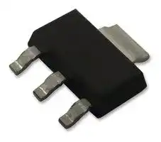
Power MOSFET, P Channel, 250 V, 260 mA, 12 ohm, SOT-223, Surface Mount
- Manufacturer: INFINEON
- Product type: Single MOSFETs
- Transistor Polarity:P Channel; Continuous Drain Current Id:-260mA; Drain Source Voltage Vds:-250V; On Resistance Rds(on):7.5ohm; Rds(on) Test Voltage Vgs:-10V; Threshold Voltage Vg
- MSL: MSL 1 - Unlimited
- SVHC: No SVHC (25-Jun-2025)
- No. of Pins: 4Pins
- Channel Type: P Channel
- Product Range: SIPMOS
- Qualification: AEC-Q101
- Power Dissipation: 1.8W
- Transistor Mounting: Surface Mount
- Rds(on) Test Voltage: 10V
- Transistor Case Style: SOT-223
- Drain Source Voltage Vds: 250V
- Operating Temperature Max: 150°C
- Continuous Drain Current Id: 260mA
- Drain Source On State Resistance: 12ohm
- Gate Source Threshold Voltage Max: 1.5V
| Delivery and price | |
|---|---|
| Units per pack | 500 |
| Price | 0.278 € |
| Current stock | 500+ |
| Lead time | 30 days |
**BSP92P** ## **SIPMOS[] Small-Signal-Transistor** **==> picture [112 x 72] intentionally omitted <==** **----- Start of picture text -----**<br> ||||| |---|---|---|---| |Product Summary| |V|DS|-250|V| |R|12|Ω| |DS(on)| |I|D|-0.26|A| **----- End of picture text -----**<br> ## **Feature** - P-Channel - Enhancement mode - Logic Level **==> picture [489 x 138] intentionally omitted <==** **----- Start of picture text -----**<br> • d d v /d t rated PG-SOT223<br>Drain<br>pin 2/4 4<br>• ¢ Pb-free Pb-free Qualified according to AEC Q101 lead plating; ROHS compliant ROHS compliant compliant Gate a J<br>pin1<br>Halogenfree according to IEC61249221 Source 3<br>ZED Rots pin 3 QeLE 2<br>1 VPS05163<br>Type Package Pb-free Tape and Reel Information Marking<br>BSP92P PG-SOT223 Yes H6327: 1000 pcs/reel BSP92P<br>**----- End of picture text -----**<br> - d d _v_ /d _t_ rated - ¢ Pb-free Pb-free Qualified according to AEC Q101 lead plating; ROHS compliant ROHS compliant compliant - Halogenfree according to IEC61249221 ## **Packaging** Non dry **Maximum Ratings** , at _T_ j = 25 °C, unless otherwise specified **==> picture [485 x 285] intentionally omitted <==** **----- Start of picture text -----**<br> ||||||||||| |---|---|---|---|---|---|---|---|---|---| |Parameter|Symbol|Value|Unit| |Continuous drain current|I|D|A| |T|A=25°C|-0.26| |T|A=70°C|-0.23| |Pulsed drain current|I|-1.04| |D puls| |T|A=25°C| |Reverse diode d|v|/d|t|d|v|/d|t|6|kV/µs| |I|S=-0.26A,|V|DS=-200V, d|i|/d|t|=-200A/µs,|T|jmax=150°C| |Gate source voltage|V|GS|±20|V| |Power dissipation|P|tot|1.8|W| |T|A=25°C| |Operating and storage temperature|T|j ,|T|stg|-55... +150|°C| |IEC climatic category; DIN IEC 68-1|55/150/56| |ESD Class| |Class 1a| |JESD22-A114-HBM| **----- End of picture text -----**<br> 2012-11- 26 Rev 2.7 Page 1 **BSP92P** **Thermal Characteristics** |**Thermal Characteristics**|| |---|---| |**Parameter**<br>**Characteristics**<br>~~ee ~~|**Symbol**<br>**Values**<br>**Unit**<br>**min.**<br>**typ.**<br>**max.**<br> ~~ee~~| |Thermal resistance, junction - soldering point|_R_thJS<br>-<br>15<br>25<br>K/W| |(Pin 4)|| |SMD version, device on PCB:|_R_thJA| |@ min. footprint|-<br>80<br>115| |@ 6 cm2cooling area1)|-<br>48<br>70| |**Electrical Characteristics**, at_T_j= 25 °C, unless otherwise specified<br>**Parameter**<br>**Symbol**<br>**Values**<br>**Unit**<br>**min.**<br>**typ.**<br>**max.**<br>**Static Characteristics**<br>~~ee~~<br>~~ee ee~~|| |Drain-source breakdown voltage<br>_V_GS=0,_I_D=-250µA<br>Gate threshold voltage,_V_GS=_V_DS<br>_I_D=-130µA<br>Zero gate voltage drain current<br>_V_DS=-250V,_V_GS=0,_T_j=25°C<br>_V_DS=-250V,_V_GS=0,_T_j=150°C<br>Gate-source leakage current<br>_V_GS=-20V,_V_DS=0<br>Drain-source on-state resistance<br>_V_GS=-2.8V,_I_D=-0.025A<br>Drain-source on-state resistance<br>_V_GS=-4.5V,_I_D=-0.23A<br>Drain-source on-state resistance<br>_V_GS=-10V,_I_D=-0.26A|_V_(BR)DSS<br>-250<br>-<br>-<br>V<br>_V_GS(th)<br>-1<br>-1.5<br>-2<br>_I_DSS<br>-<br>-<br>-0.1<br>-10<br>-0.2<br>-100<br>µA<br>_I_GSS<br>-<br>-10<br>-100<br>nA<br>_R_DS(on)<br>-<br>10<br>20<br>Ω<br>_R_DS(on)<br>-<br>8.2<br>15<br>_R_DS(on)<br>-<br>7.5<br>12<br>po} tt<br>| |<br>fT|<br>ttt<br>|<br>|tf<br>| |tt<br>|<br>|tf<br>|tf| 1Device on 40mm*40mm*1.5mm epoxy PCB FR4 with 6cm² (one layer, 70 µm thick) copper area for drain connection. PCB is vertical without blown air. 2012-11- 26 Rev 2.7 Page 2 **BSP92P** |**Electrical Characteristics**, at_T_j= 25 °C, unless otherwise specified<br>**Parameter**<br>**Symbol**<br>**Dynamic Characteristics**<br>~~ee~~|**Electrical Characteristics**, at_T_j= 25 °C, unless otherwise specified<br>**Parameter**<br>**Symbol**<br>**Dynamic Characteristics**<br>~~ee~~|**Electrical Characteristics**, at_T_j= 25 °C, unless otherwise specified<br>**Parameter**<br>**Symbol**<br>**Dynamic Characteristics**<br>~~ee~~|**Electrical Characteristics**, at_T_j= 25 °C, unless otherwise specified<br>**Parameter**<br>**Symbol**<br>**Dynamic Characteristics**<br>~~ee~~|= 25 °C, unless otherwise specified<br>**Conditions**<br>**Values**<br>**Unit**<br>**min.**<br>**typ.**<br>**max.**<br>~~el~~|= 25 °C, unless otherwise specified<br>**Conditions**<br>**Values**<br>**Unit**<br>**min.**<br>**typ.**<br>**max.**<br>~~el~~|= 25 °C, unless otherwise specified<br>**Conditions**<br>**Values**<br>**Unit**<br>**min.**<br>**typ.**<br>**max.**<br>~~el~~|= 25 °C, unless otherwise specified<br>**Conditions**<br>**Values**<br>**Unit**<br>**min.**<br>**typ.**<br>**max.**<br>~~el~~|= 25 °C, unless otherwise specified<br>**Conditions**<br>**Values**<br>**Unit**<br>**min.**<br>**typ.**<br>**max.**<br>~~el~~| |---|---|---|---|---|---|---|---|---| |Transconductance<br>Input capacitance<br>Output capacitance<br>Reverse transfer capacitance<br>Turn-on delay time|_g_fs<br>|_V_DS|≥2*|_I_D|*_R_DS(on)max ,<br>_I_D=-0.23A<br>0.29<br>0.57<br>-<br>_C_iss<br>_V_GS=0,_V_DS=-25V,<br>_f_=1MHz<br>-<br>83<br>104<br>_C_oss<br>-<br>13<br>16<br>_C_rss<br>-<br>6<br>8<br>_t_d(on)<br>_V_DD=-125V,_V_GS=-10V,<br>-<br>5<br>8<br>oonne<br>=—_===|||||||S<br>pF<br>ns| |Rise time||_t_r||_I_D=-0.26A,_R_G=6Ω|-|6|9|| |Turn-off delay time||_t_d(off)|||-|67|101|| |Fall time||_t_f|||-|33|50|| |**Gate Charge Characteristics**||||||||| |Gate to source charge||_Q_gs||_V_DD=-200V,_I_D=-0.26A|-|-0.1|-0.13|nC| |Gate to drain charge||_Q_gd|||-|-1.9|-2.4|| |Gate charge total||_Q_g||_V_DD=-200V,_I_D=-0.26A,|-|-4.3|-5.4|| |||||_V_GS=0 to -10V||||| |Gate plateau voltage||_V_(plateau)||_V_DD=-200V,_I_D=-0.26A|-|-2.9|-3.6|V| |**Reverse Diode**||||||||| |Inverse diode continuous||_I_S||_T_A=25°C|-|-|-0.26|A| |forward current||||||||| |Inv. diode direct current, pulsed||_I_SM|||-|-|-1.04|| |Inverse diode forward voltage||_V_SD||_V_GS=0,_I_F=-0.26A|-|-0.83|-1.21|V| |Reverse recovery time||_t_rr||_V_R=-125V,_I_F=_l_S,|-|51|64|ns| |Reverse recovery charge||_Q_rr||d_i_F/d_t_=100A/µs|-|76|95|nC| 2012-11- 26 Rev 2.7 Page 3 **BSP92P** ## **1 Power dissipation** _P_ tot = _f_ ( _T_ A) ## **2 Drain current** _I_ D = _f_ ( _T_ A) parameter: | _V_ GS| ≥ 10V **==> picture [480 x 266] intentionally omitted <==** **----- Start of picture text -----**<br> BSP 92 P BSP 92 P<br>W1.9 S ESS -0.28A<br>Cee Ae<br>1.6 PCCPFCOREEEEEEEEE Eee -0.24 LEPINE\ EEE<br>-0.22<br>1.4<br>SEEEERPLT ENE EEE -0.2 LETNET TT T TT<br>1.2 ECOCCAREPETA R E TTTC E P -0.18 EEETTT\<br>-0.16<br>KEE TT ENE<br>1 EERE EEE ENE<br>-0.14<br>ECCECC EP NEC Err \<br>EEE EEE PP EEE LETTE<br>0.8 -0.12<br>f CoN fo -0.1 ETT IN<br>0.6 RAE TTT<br>EECEEE EEN -0.08 TT TT TT EN |<br>PECTIN Tr PITTI<br>0.4 -0.06<br>HET TTT TET ET AE<br>-0.04<br>FEE EEE PEN TT TET TT TT TT Ty TT<br>0.2<br>FCCC E EE E EECee -0.02 EEE EE<br>0 ECCCCCCE rN 0 PIT ETT TETT [TTT]<br>0 20 40 60 80 100 120 °C 160 0 20 40 60 80 100 120 °C 160<br>T A T A<br>tot<br>P I D<br>**----- End of picture text -----**<br> ## **3 Safe operating area** _I_ D = _f_ ( _V_ DS ) parameter : _D_ = 0 , _T_ A = 25°C **==> picture [235 x 266] intentionally omitted <==** **----- Start of picture text -----**<br> -10 1 BSP 92 P<br>A<br>-10 0 Samet (0 t p = 110.0 aa µs<br> 1 ms<br>I AN CIN Nl<br>-10 -1 10 ms<br>-10 -2 mr<br>DC<br>SEH Ste<br>| TTT TTT PTT<br>-10 -3 UNI TTP I<br>-10 [-1 ] -10 [0 ] -10 [1 ] -10 [2 ] V -10 [3 ]<br>V DS<br>I D<br> /<br>V DS<br> =<br>R DS(on)<br>D<br>I<br>**----- End of picture text -----**<br> ## **4 Transient thermal impedance** _Z_ thJA = _f_ ( _t_ p) parameter : _D_ = _t_ p/ _T_ **==> picture [233 x 268] intentionally omitted <==** **----- Start of picture text -----**<br> 10 2 BSP 92 P<br>K/W<br>10 1 i mm<br>eS SSH<br>10 0<br>D = 0.50<br>0.20<br>single pulse 0.10<br>0.05<br>10 -1 A iy TPH i<br>0.02<br>avi at an a a 0.01<br>LATTICE TTT TTT TTA TTI TTT toc<br>10 -2 SUING<br>IN TNS<br>10 [-5 ] 10 [-4 ] 10 [-3 ] 10 [-2 ] 10 [-1 ] 10 [0 ] 10 [1 ] 10 [2 ] s 10 [4 ]<br>t<br>—_ p<br>thJA<br>Z<br>**----- End of picture text -----**<br> 2012-11-26 Rev 2.7 Page 4 **BSP92P** ## **5 Typ. output characteristic** _I_ D = _f_ ( _V_ DS) parameter: _T_ j =25°C, - _V_ GS ## **6 Typ. drain-source on resistance** _R_ DS(on) = _f_ ( _I_ D) parameter: _V_ GS; _T_ j =25°C, - _V_ GS **==> picture [479 x 262] intentionally omitted <==** **----- Start of picture text -----**<br> 1 18<br>A 10V Ω 2.6V 2.8V 3.2V<br>JL eer<br>6V<br>5V<br>0.8 4.6V 14<br>4.2V — _ SRieeeee<br>0.7 3.6V<br>3.4V 12<br>0.6 3.2V i<br>2.8V 10<br>2.6V i”) ZaZ A ae<br>0.5<br>8<br>0.4 10V<br>I fC ee 6V<br>6<br>0.3 py Of LOT NSS 5V<br>4.6V<br>0.2 fe 4 4.2V<br>3.6V<br>0.1 foZCCCeeEe] 2 TEEEEELS 3.4V<br>0 0<br>0 1 2 3 4 5 6 7 8 V 10 0 0.1 0.2 0.3 0.4 0.5 0.6 0.7 0.8 A 1<br>- V DS -I D<br>D DSON<br>I - R<br>**----- End of picture text -----**<br> ## **7 Typ. transfer characteristics** _I_ D= _f_ ( _V_ GS ); | _V_ DS|≥ 2 x | _I_ D| x _R_ DS(on)max parameter: _T_ j = 25 °C **==> picture [223 x 262] intentionally omitted <==** **----- Start of picture text -----**<br> 1<br>A<br>Bans<br>|<br>0.6<br>| | yp)<br>0.4 tA |<br>0.2 ety}<br>0<br>0 1 2 V 4<br>- V GS<br>D<br>I -<br>**----- End of picture text -----**<br> ## **8 Typ. forward transconductance** _g_ fs = f( _I_ D) parameter: _T_ j =25°C **==> picture [222 x 262] intentionally omitted <==** **----- Start of picture text -----**<br> 1<br>S<br>BEEBE<br>0.6<br>L AT LL<br>0.4 AL<br>0.2 ELLE<br>0<br>0 0.2 0.4 0.6 A 1<br>- I D<br>fs<br>g<br>**----- End of picture text -----**<br> 2012-11- 26 Rev 2.7 Page 5 **BSP92P** ## **10 Gate threshold voltage** ## **9 Drain-source on-state resistance** _R_ DS(on) = _f_ ( _T_ j) _V_ GS(th) = _f_ ( _T_ j) parameter: _V_ GS = _V_ DS ; _I_ D = -130µA parameter : _I_ D = -0.26 A, _V_ GS = -10 V **==> picture [282 x 267] intentionally omitted <==** **----- Start of picture text -----**<br> BSP 92 P<br>32<br>Ω PPLELLLELLLI<br>POCELClE Ele<br>fooeeeeeee<br>24 POCEECle ee ee<br>PCE eee<br>20 Pi Peer eer<br>FECEEELL tert, Let<br>16<br>POCELLCOPLEE<br>98%<br>SA er<br>12<br>H ER R tf<br>POET CCE TT<br>8 typ<br>OEEeer e CEPre<br>4 eT C LE<br>F t POCELClEeeer tt tT ET ELT<br>0<br>-60 -20 20 60 100 °C 180<br>T<br>—_ j<br>DS(on) V GS(th)<br>R -<br>**----- End of picture text -----**<br> **==> picture [227 x 263] intentionally omitted <==** **----- Start of picture text -----**<br> 2.2<br>V<br>TAIT TTT).<br>on<br>98%<br>1.8<br>aS eee<br>:<br>mT}<br>1.6<br>| |] ) RAL<br>typ.<br>PT oM™ALT<br>1.4<br>TTT RAT<br>1.2<br>Ne<br>tf SERCO<br>1 2%<br>.<br>0.8<br>Ty taL E<br>Py TEL TTL PASE<br>0.6 TET TTY Pye<br>0.4<br>-60 -20 20 60 100 °C 160<br>T<br>—_ j<br>GS(th)<br>V<br>-<br>**----- End of picture text -----**<br> ## **11 Typ. capacitances** ## _C_ = _f_ ( _V_ DS) parameter: _V_ GS=0, _f_ =1 MHz, _T_ j = 25 °C **==> picture [225 x 266] intentionally omitted <==** **----- Start of picture text -----**<br> 10 3<br>============<br>pF ee GsGQ GO<br>CCOCEECEEEEErt | [| [| | [| [ | | fT t<br>Ciss<br>10 2<br>ATT Et Ef |<br>—————_——<br>AN eG<br>2 eee<br>Coss<br>f 10 1 (NEEREEQe EE<br>=<br>a ee en OO<br>Crss<br>Sette<br>10 0 CCEAEo<br>0 6 12 18 24 V 36<br>- V DS<br>C<br>**----- End of picture text -----**<br> ## **12 Forward character. of reverse diode** _I_ F = _f_ (VSD) parameter: _T_ j **==> picture [224 x 266] intentionally omitted <==** **----- Start of picture text -----**<br> -10 1 BSP 92 P<br>======—==SSSSSe<br>A Ct tT ft tT yy yy<br>eeeFEC<br>-10 0<br>LEE<br>SS<br>ee ee ae eee<br>eee Ane<br>-10 -1 S007 4S<br>of GOW<br>T j = 25 °C typ<br>See ==<br>LC | Tee TE T j = 150 °C typ [ [ | |<br>T j = 25 °C (98%)<br>| ATS T j = 150 °C (98%) L | tt<br>-10 -2 tsCTTAT Tr<br>0 -0.4 -0.8 -1.2 -1.6 -2 -2.4 V -3<br>V SD<br>F<br>I<br>**----- End of picture text -----**<br> 2012-11- 26 Rev 2.7 Page 6 **BSP92P** ## **13 Typ. gate charge** ## _V_ GS = _f_ ( _Q_ Gate) ## **14 Drain-source breakdown voltage** _V_ (BR)DSS = _f_ ( _T_ j) ## parameter: _I_ D = -0.26 A pulsed **==> picture [482 x 267] intentionally omitted <==** **----- Start of picture text -----**<br> BSP 92 P BSP 92 P<br>-16 -300<br>FCELELELL ELLE V TET<br>V<br>PTT ETT ETT Taye PEE<br>PT TTT TT TT YA tf -285 PT<br>HA PELL<br>-12 AAA CEE<br>-280<br>HAA E PPE<br>-275<br>Lehi} SEEPS<br>-10 AA Seeeeeee<br>-270<br>FEELELIA eee<br>ELT SSPE<br>-265<br>-8 20% FLELVYAZ_LEL VA<br>NLS Po -260 PT tT Tey yy<br>50%<br>-255<br>-6 80%<br>Si0//AnEnene | PP tT tT AT Ty<br>N/R -250 PL TT yA<br>-4 ORY -245 PL i JAT TT Tt<br>PELVAYEE LEE -240 Pt vA et<br>-2 (ce -235 ATTY<br>PCCCELEE EL -230 ALCP Eee<br>0 PCEEELELE ELLE -225 PEEP EEE<br>0 1 2 3 4 5 nC 6.5 -60 -20 20 60 100 °C 180<br>|Q G | T j<br>GS (BR)DSS<br>V V<br>**----- End of picture text -----**<br> 2012-11- 26 Rev 2.7 Page 7 **BSP92P** 2012-11- 26 Rev 2.7 Page 8
Updated at April 29, 2026
Infineon Technologies is a globally recognized leader in semiconductor solutions, renowned for driving innovation in power management, energy efficiency, and modern mobility. With a strong legacy of engineering excellence, the company provides highly reliable components designed to meet the rigorous demands of industrial, automotive, and advanced commercial applications. The core of our Infineon portfolio is centered on their industry-leading discrete semiconductors. We offer an extensive selection of single and dual MOSFETs, alongside a robust range of single IGBTs and advanced IGBT modules. These flagship power transistors are essential for high-efficiency power conversion and motor control, providing engineers with superior thermal performance and minimized switching losses. Beyond advanced field-effect transistors, the selection includes a comprehensive array of diodes and rectifiers, heavily featuring Schottky diodes, as well as fast-recovery and RF/PIN diodes. This power foundation is further supported by bipolar transistors, intelligent power modules, and thyristor SCR modules, delivering the critical building blocks required for complex power system designs. To support broader system integration, the portfolio also encompasses specialized solutions such as solid-state relays, AC/DC LED driver ICs, and Bluetooth communications modules. From high-power industrial rectifiers to wireless connectivity adapters, Infineon equips designers with the precision components needed to build efficient, scalable, and fully connected electronic systems.
About Novapart
Novapart is a B2B electronic component broker specialising in stock shortages and cost reduction. We source hard-to-find parts and identify compliant alternatives across a catalogue of 410,000+ components from 500+ manufacturers.
Learn more →Stock Shortage Specialist
When a component is unavailable, discontinued or has an unacceptable lead time, we tap into our network of vetted European and Asian distributors to source what you need — without compromising on quality or traceability.
Request a quote →Compliant Alternatives
We identify pin-to-pin, electrically equivalent substitutes that meet the same certifications (RoHS, AEC-Q100, REACH) as your original specification — validated against datasheets, not just part numbers. Often at a lower cost.
BOM Analysis service →